Introduction
The widespread adoption of mobile devices and high data rate applications, such as virtual and augmented reality, has significantly increased the demands on mobile network systems. Millimeter-wave (mmW) bands have emerged as a key solution for meeting these demands by optimizing data throughput, latency, and energy efficiency while maintaining a seamless user experience. Owing to their larger continuous bandwidth (BW), mmW bands enable higher data transmission rates and lower latency with high spectrum efficiency. However, mmW band transmission signals face several challenges, including significant propagation loss, high sensitivity to obstacle blockages, and directivity issues owing to their short wavelength. To address these limitations, technologies such as beamforming, based on active phased array antenna (APAA) architectures and small-cell networks have been developed. A previous study has demonstrated that mmW bands in 5G networks offer potential advantages in data throughput and power consumption compared to sub-6 GHz frequencies under specific conditions [Reference Brambilla, Cerutti, Colombo and Tornatore1]. Consequently, 28 and 39 GHz radio frequency (RF) modules and radio units (RUs) have become increasingly common in mobile devices and base stations (BSs) [Reference Dunworth, Homayoun, Ku, Ou, Chakraborty, Liu, Segoria and Aparin2–Reference Kim, Park, Song, Moon, Kim, Kim, Chang and Ho5]. However, conventional mmW RUs often face limitations, including large size, high cost, and low energy efficiency, making them less suitable for deployment in 5G New Radio (NR) small-cell networks. A primary factor restricting RU size reduction is the array antenna size, which depends on the frequency band and the number of antennas needed to compensate for the significant propagation loss associated with mmW bands. The 3GPP 5G NR standard defines mmW bands ranging from 24.25 to 52.6 GHz, with the 47 GHz band drawing particular attention. Its shorter wavelength allows for more compact RUs, and it is readily available within the 5G mmW bands.
Conventional very large-scale APAA modules in mmW RU employ antenna on board (AoB) technology, which requires complex board design and integration. However, AoB faces several challenges, including large feeder line losses owing to the relatively thick board and complex integration requirements. It is also unsuitable for RFs above 47 GHz. To address these limitations, CMOS-based phased array transceivers with embedded antenna in package using fan-out wafer-level packaging (AiP-FOWLP) technology can offer lower feeder line loss, easier integration, lower cost, and better scalability for mass production. However, conventional AiP-FOWLP structures are hindered by high thermal resistance, which can lead to mechanical damage and electrical performance degradation, making them unsuitable for constructing tile-based very large-scale APAA modules [Reference Che and Chen6]. In addition, power-added efficiency in CMOS power amplifiers remains low, typically less than 10%, owing to the high peak-to-average power ratio requiredby 5G NR modulation schemes and the size constraints of phased array transceiver chips [Reference Sadhu, Tousi, Hallin, Sahl, Reynolds, Renström and Valdes-Garcia7]. With most DC power converted to heat, effective thermal management becomes essential.
CMOS-based phased array transceivers employing a facing-up (FU) AiP-FOWLP design address these issues by offering high power efficiency, simplified thermal management, design optimization, miniaturization, low cost, and scalability for mass production. This configuration is one of the strongest solutions for constructing compact tile-based, very large-scale APAA modules.
This paper describes a compact 47 GHz dual-polarized, 32-element phased array transceiver with FU AiP-FOWLP architecture for the 5G NR band n262, which is from 47.2 to 48.2 GHz. It demonstrates high equivalent isotropic radiated power (EIRP), low error vector magnitude (EVM) under 5G NR modulation schemes, precise beamforming capability, and a high heat dissipation package. An earlier version of this paper was presented at the 2024 19th European Integrated Circuits Conference (EuMIC) and was published in its proceedings [Reference Kobayashi, Shimura, Yagishita, Nishimori, Ohashi, Kawano and Suzuki8].
47 GHz dual polarized 32-element phased array transceiver and FU AiP-FOWLP
CMOS-based phased array transceiver and FU AiP-FOWLP
Figure 1 shows the block diagram of the proposed phased array transceiver chip. The transceiver chip has 16 channel transceivers in each horizontal (H) and vertical (V) polarization, and it implements serial peripheral Interface to control beam directions and can offer the ability to support beam forming and MIMO. The chip consists of 32 TRx paths, two 1:16 intermediate frequency (IF) distributors, a local oscillator (LO) signal chain, and a control module. Each TRx path has an RF front end (RFFE), a bidirectional IF vector-sum phase shifter (VSPS), and an IQ mixer. The LO signal chain includes a x4 frequency multiplier, a 1:2 power distributor, and two 1:16 power distributors, which deliver LO power to each mixer. To meet the spurious emission requirement of Pspurious = −13 dBm/MHz, the IF center frequency was designed to be 7.5 GHz. This choice considered the gain bandwidth of the PA, the LO frequency, and the potential for undesired spurious signals from the frequency multiplier. The LO frequency is capable of operating within the range of 9.225–10.175 GHz. The control module features a high-resolution digital-to-analog converter (DAC) that supplies voltage bias for the IF VSPS and RFFE, SRAM that stores the bias voltage conditions for each VSPS based on beam IDs, and a low-speed analog to digital for monitoring output power variations of each transmitter and die temperatures caused by environmental and power supply voltage changes. The transceiver is fabricated using a 55-nm bulk CMOS process and employs a bidirectional IF phase-shifting architecture that achieves high phase resolution, accurate performance, and compact size. Figure 2 shows a microphotograph of the 9.1 mm × 11.7 mm transceiver chip including bump pads.
Block diagram of the 47-GHz dual-polarized, 32-element phase array transceiver.

Microphotograph of the 47-GHz dual-polarized, 32-element phased array transceiver.

Figure 3 shows a detailed RF, IF, LO, and DC signal flow, as well as cross-sectional view of the FU AiP-FOWLP structure. This structure features the CMOS circuit and antenna on the top side to minimize feeder line losses and thermal resistance. The package utilizes a five-metal-layer and four-redistribution-layer (RDL) structure. The antenna and RF port of the phased array transceiver are connected using impedance-controlled lines and vias in a multi-layer interconnect, achieving high signal-to-signal isolation while minimizing insertion loss. Figure 4 shows a photograph of the 4 × 4 path antenna array and the ball grid array (BGA) side of the FU AiP-FOWLP. The antenna employs a square patch, and the feed points are offset both vertically (V) and horizontally (H) from the central of the element, allowing for dual-polarization. The antenna element space of d is set to a half wavelength to avoid limitations in the scanning range owing to grating lobes. The solder balls, with a diameter of 330 μm, are arranged on a 500-μm pitch to improve the thermal resistance. H/V polarization IF and LO signals are assigned to the outermost ring of solder balls within the BGA. These solder balls employ a GSG (Ground-Signal-Ground) configuration to maintain characteristic impedance and minimize loss up to 11 GHz. Power and Ground signals are assigned to the remaining solder balls within the outermost ring and the ring immediately inside it of the BGA. The solder balls in the central area act as heat spreaders, resulting in a package thermal resistance of less than 0.3 K/W.
Cross-sectional view of the FU AiP-FOWLP structure.

Photograph of the FU AiP-FOWLP structure. (a) Antenna side. (b) BGA side.

Bidirectional IF phase shifter and IQ mixer
The high-resolution compact phase shifter is a critical component for realizing the compact dual-polarized, 32-element phased array transceiver. It must meet stringent requirements, including a phase switching time within 100 ns to suppress transmission rate degradation caused by beam switching delays. It also requires a phase resolution of 2.8° with root mean square less than 1.4° rms for phase accuracy and 0.25 dB for amplitude accuracy to enable high-precision beam scanning. Various analog and digital phase-shifting architectures have been proposed, such as passive phase shifters with a switch [Reference Duan, Chen, Mao, Zou, Li, Feng, Wang and XL9], LO-based phase shifting [Reference Pang, Wu, Wang, Dome, Kato, Huang, Narayanan and Okada10], and VSPS consisting of a variable gain amplifier (VGA) [Reference Shimura, Ohshima and Ohashi11]. VSPS with a high-bit DAC can deliver high-resolution phase and amplitude control with low deviation and power consumption. The bidirectional IF phase shifter with frequency conversion can reduce implementation area while maintaining phase resolution and gain deviation. The block diagram of the proposed quadrature IF phase shifter, along with the IQ plane and frequency domain signal flow, is shown in Fig. 5. The higher available gain and isolation characteristics of FETs in low frequency, compared to high frequency, allows for the realization of a compact and switchless bidirectional VGA with high dynamic range, using lumped components. The bidirectional IQ VGA consists of a bidirectional differential buffer amplifier, a polyphase filter, and two bidirectional zero-pi VGAs. For Tx, the signal flow begins with a polyphase filter generating quadrature phase signals from the input IF signal. These quadrature signals are amplitude-shifted by the I and Q paths of the zero-pi VGA. Next, the IF signals are converted to RF signals by an IQ mixer and combined at each output. An on-chip transformer balun converts from differential signal to single-ended signal. Rx operates in reverse. To achieve a phase resolution of less than 1° with a quadrature phase shifter, between I and Q vector ratio and magnitude resolution step are crucial. The output phase θ out is expressed by magnitude Q and I vector.
 \begin{equation}{\theta _{out}} = tan{h^{ - 1}}\left( {\frac{Q}{I}} \right)\end{equation}
Block diagram of the proposed IF phase shifter, IQ plane, and frequency domain signal flow.

From equation (1), the gain dynamic range of bidirectional zero-pi VGA requires more than 36 dB to realize less than 1° output phase. To maintain a phase resolution of 1° between 0° and 90°, digital bit number N needs to be greater than 7, as calculated by the simple equation 90°/2 N, which implies that linear gain control of bidirectional zero-pi VGA needs to be less than 0.28 dB. The bidirectional IQ VGA is realized using a digitally assisted bidirectional zero-pi VGA operating at 7.5 GHz. Figure 6 shows a schematic of a unidirectional zero-pi VGA and a block diagram of a bidirectional zero-pi VGA. The unidirectional zero-pi VGA consists of a power switch transistor Mp1, two load inductors LS, a cross-coupled common source amplifier with four gm transistors Mn1–Mn4, two tail transistors Mn5 and Mn6, and a 10-bit voltage DAC. For enabled the zero mode, a current ISS flows through the tail current source transistor Mn3, and a current ISS/2 flows through the cross-coupled transistors Mn1 and Mn2. The differential small signal voltage gains AV at low frequency express following equation.
 \begin{equation}\left| {{A_V}} \right| = \sqrt {{\mu _n}{C_{ox}}\frac{W}{L}{I_{SS}}} {Z_L}\end{equation}
Schematic of the unidirectional zero-pi VGA and block diagram of the zero-pi bidirectional VGA.

where μn denotes the nch mobility, Cox denotes the gate capacitance per unit area, W denotes the gate width, L denotes the nch gate length, and ZL denotes the load impedance of the common source amplifier. From equation (2), the gain of a differential common source amplifier can be tuned by the tail current ISS. The 10-bit DAC, with a full-scale voltage 1.2 V, is adopted to precisely control the gate-to-source voltage of tail transistors allowing exceptionally fine linear gain adjustments with steps below 0.28 dB. While the DAC has 10-bit resolution, the VGA control utilizes a 7-bit control, providing a gain control step of 0.28 dB and sufficient margin to account for process variations and temperature effects, enabling fine-grained phase adjustments. To achieve a dynamic gain range over 36 dB, a two-stage VGA is employed. The zero-pi switching function is achieved by the cross-couple connection of the gm transistors and the tail transistor switching. Additionally, the power switch Mp1 supplies 1.2 V to the unidirectional VGA, following the control signal. The bidirectional zero-pi VGA consists of two four-stage unidirectional zero-pi VGAs connected in an antiparallel configuration. When the circuit receives control signals, one of the four-stage unidirectional VGAs is activated, while the other is disabled. The disabled VGA remains in an OFF state and introduces capacitive load at the input and output. To minimize the adverse effects of these capacitive loads, the transistor sizes for both the input and output stages of the zero-pi VGA are carefully selected.
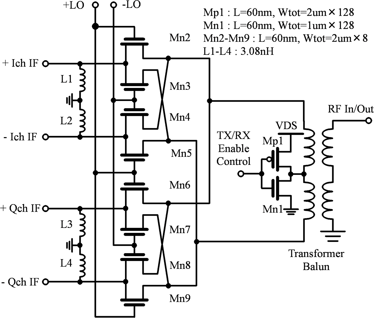
A high conversion gain, high linearity, and compact implementation area are critical features for the bidirectional IQ mixer in achieving the proposed IF phase shifter’s functionality. In addition, reducing the power consumption and implementation area of the PA is essential for improving energy efficiency and reducing the overall chip size. Notably, the mixer’s conversion gain and linearity in Tx mode are key to easing the PA’s performance requirements. Many bidirectional mixers have been proposed and studied [Reference Weng, Shen and Chang12, Reference Parlak and Buckwalter13]. Conventional resistive mixers are well-suited for achieving high linearity and bidirectional operation. However, they suffer from high CL and require a large LO driving power. On the other hand, Gilbert cell-based bidirectional mixers offer lower CL and require lower LO driving power. Nevertheless, their linearity falls short compared to resistive ring mixers [Reference Chang and Lin14]. A resistive mixer with a selective drain bias, which improves the CL and linearity, is reported in paper [Reference Garcia, Pedro, De La Fuente, De Carvalho, Sánchez and Puente15]. Figure 7 shows a schematic of the proposed IQ mixer, which provides bidirectional frequency conversion with a selective drain bias. The IQ mixer comprises switching stage transistors (Mn2–Mn9) arranged in two double-balanced resistive mixer configurations, a drain bias switch (Mp1 and Mn1), matching and DC feed inductors (L1–L4), and an on-chip transformer balun at the RF port. Leveraging a modified double-balanced topology with a power switch added to the center tap of the balun design successfully facilitates efficient bidirectional up or down frequency conversion. The frequency conversion of the resistive mixers is driven by transistor drain modulation in the presence of an RF signal at the drain or source terminal and sufficient LO driving power at the gate terminal. However, signal-to-noise distortion ratio degradation occurs owing to third-order intermodulation (IM3) from the third-order drain conductance (Gd3) and the gate–source and gate–drain capacitance nonlinearity. To achieve low IM3 and maintain high performance, minimizing Gd3 becomes essential when nonlinear capacitance effects at RFs are negligible. The Gd3 at low frequency is expressed as shown in equation (3).
 \begin{equation}{G_{d3}} = \frac{1}{{12}} \cdot \frac{{{\partial ^3}{G_{ds}}}}{{\partial {V_{ds}}^3}}\end{equation}
Bidirectional IQ mixer with a drain bias switch.

where Gds is the first-order drain conductance. Figure 8 illustrates the results of DC simulations of Gd3 under different drain bias conditions. Compared to when Vds = 0 V, the simulated Gd3 with Vds = 0.6 and 1.2 V demonstrates significant improvement across the bias voltage range from Vgs = 0 V to Vgs = 1.2 V. This result indicates that applying a large drain bias effectively reduces IM3 products. In the Tx mode, the power switch is set to 1.2 V. During this operation, the bleeding current flows through the balun, the switching-stage transistors, and the inductors, while the switch-stage transistors are biased with a large drain–source voltage. This large drain–source voltage improves Gds3, effectively reducing the IM3 products by the switching current. In addition, the bleeding current enhances the CG. Conversely, in the Rx mode, the power switch is set to 0 V to enable efficient bidirectional conversion. Under this mode, the switch-stage transistors operate as a classical resistive mixer. This operating mode has a large CL and low linearity compared to the Tx mode.
VGS dependency of simulated Gd3 with VDS = 0, 0.6, 1.2 V.

Measurement results
On-wafer measurements
Figure 9 shows a microphotograph of the bidirectional IF VSPS and IQ mixer, with a core area measuring 510 μm × 680 μm On-wafer measurements were conducted to evaluate the performance of the IQ mixer and the IF phase shifter. A 360°-state constellation diagram, captured after amplitude calibration of the I and Q paths at 43 GHz, is presented in Fig. 10. The measured rms phase error is 0.447°, and the rms amplitude error is 0.063 dB, with a phase resolution of 1°. Figure 11(a) shows the measured CG and third-order intercept point (TOI), while Fig. 11(b) displays the measured IM3 characteristics of the IF phase shifter and IQ mixer in Tx mode. To analyze the CG and TOI under different bias conditions, the node voltage of the center tap of the transformer balun was biased at 0 and 1.2 V. When the center tap is biased at 0 V, the mixer operates as a traditional resistive mixer. When biased at 1.2 V, the mixer operates in the proposed mode. The measurements were performed over the entire RF range from 47 to 49 GHz, at a fixed IF frequency of 7.5 GHz. The CG and TOI measurements for the 1.2-V biased IQ mixer demonstrate improved performance across the tested RFs. Specifically, at 47 GHz, the IM3 measurements show that the 1.2 V-biased configuration achieves an approximate 10 dB improvement over the 0 V-biased configuration. Therefore, applying a large drain–source bias voltage to the resistive IQ mixer improves the CG and IM3 products.
Microphotograph of the bidirectional IF VSPS and IQ mixer.

Measured 360°-state constellation diagram.

Measured characteristics of bidirectional IF VSPS and IQ mixer in the Tx mode. (a) CG and TOI with VDS = 0, 1.2 V. (b) IM3 with VDS = 0, 1.2 V.

On-wafer measurements were performed to characterize the transmitter and receiver performance of the 32-element phased array transceiver, as shown in Fig. 2. The measured characteristics of a single-element transmitter and receiver over the RF range from 47 to 49 GHz are presented in Fig. 12(a) and (b). The measured transmitter CG and EVM are around 25 dB and −30 dB at +6 dBm output power under 5G NR modulation schemes (256QAM OFDM, 100 MHz BW). The measured receiver CG and input P1dB are around 20 dB and −35 dBm, respectively. The transmitter and receiver exhibited a flat CG response over all the measured RFs.
Measured characteristics of the single element on the phased array transceiver. (a) Transmitter CG and EVM. (b) Receiver CG and input P1db.

OTA measurements
Figure 13(a) shows an AiP evaluation board for over-the-air (OTA) measurements. The V and H polarization IF ports, as well as the LO port, are connected to 50-Ω transmission lines through end-launched connectors. Figure 13(b) depicts the OTA measurement setup. The AiP evaluation board is mounted on an XY axis turntable, with a sufficient distance between the AiP and the reference antenna to ensure measurements are conducted within the far-field region.
AiP evaluation board and OTA measurement setup. (a) AiP evaluation board. (b) OTA measurement setup.

The normalized measured and simulated H polarization Tx array beam patterns in the azimuth plane for phase shifts of 0°, ±45°, ±90°, with a uniform amplitude distribution, are shown in Fig. 14(a). Beam angle measurements were conducted within a range of −60° to +60°. The results demonstrate reasonable agreement between the simulations and measurements. Consistent Tx radiation patterns were also observed for both H and V polarizations in the azimuth and elevation planes. Figure 14(b) highlights the H and V polarization beam-steering performances, achieving a scan range from −40° to +40° in both the azimuth and elevation planes. Figure 15 illustrates the two-dimensional H polarization Tx beam pattern in the boresight. The solid lines represent contour levels ranging from 35 to 0 dBm in 2.5-dB steps. The achieved peak EIRP was 30.7 dBm for the single polarization 16-element transmitters. The obtained half-power bandwidths in the elevation and azimuth plane were 28° and 27°, respectively, aligning closely with simulation results. The measured Tx 256 QAM OFDM constellation diagram is shown in Fig. 16. The obtained peak EVM was −28.1 dB under 5G NR modulation scheme (100 MHz BW) at the boresight. Table 1 summarizes the overall performance of this work and related work. The proposed IF phase shifting phased array transceiver chip achieves less than 1° phase resolution, with rms phase and amplitude errors of 0.447° and 0.063 dB, respectively. High linearity of the transmitter, achieved with the proposed IQ mixer, and high CG of receiver are realized with acceptable power consumption and a compact AiP size of only 14.9 × 12.3 mm2. The 2-m OTA measurements demonstrated, the developed 47 GHz 32-element phased array transceiver and packaged 4 × 4 antenna array with FU AiP-FOWLP demonstrated that it satisfied 5G Tx EVM requirements.
Measured Tx beam pattern performances. (a) Simulation and measured H polarization Tx beam patterns in the azimuth plane. (b) Measured H and V polarization Tx beam steering performances in the azimuth and elevation planes.

Measured two-dimensional Tx beam pattern in the boresight.

Measured Tx 256 QAM constellation diagram.

Summary of reported silicon-based mmW AiP phase array transceivers

a Peak EIRP.
b Tx system efficiency = EIRP(W)/Tx power consumption (W).
Conclusion
This paper presents a compact dual polarization 32-element 47 GHz phased array transceiver realized using low-cost 55-nm CMOS process and FU AiP-FOWLP for 5G mmW communications. The proposed bidirectional IF phase shifter and IQ resistive mixer with applying large drain bias can deliver good linearity and high CG with high phase and amplitude accuracy. The FU AiP-FOWLP achieves low thermal resistance and low feed line loss for realizing a very large scale AAPA modules. The first fully integrated 47 GHz phased array transceiver with FU AiP-FOWLP can realize high data rates and directly be used for low-cost compact RU of 5G small cell BSs.
Acknowledgements
This paper is based on results obtained from a project, JPNP20017, subsidized by the New Energy and Industrial Technology Development Organization (NEDO).
Competing interests
The authors declare none.

Jun Kobayashi received his B.E. and M.S. degrees in physics from Toho University in 2003 and 2005, respectively. He joined Fujitsu Limited in 2022, where he has been engaged in the development of millimeter-wave phased array transceiver chips for base stations in mobile wireless communication systems. He is currently focusing on the development of wireless systems for fifth-generation (5G) mobile systems.

Toshihiro Shimura received the B.E. degree in physics from the University of Tsukuba, Japan, in 1990. He joined Fujitsu Laboratories, Ltd., Kawasaki, Japan, in 1991, where he had been engaged in the research and development of millimeter-wave ICs using HEMT and CMOS technologies for automotive radar sensors and wireless communication systems. In 2019, he moved to Fujitsu Limited, where has been engaged in the development of millimeter-wave phased array transceiver ICs for mobile wireless communication systems. His current research interests include millimeter-wave beamforming ICs for massive MIMO systems, and high-power amplifier design and linearization techniques for mobile base-station systems.

Yohei Yagishita received his B.E. in electrical and electronic engineering from Ehime University in 2006 and M.S. degrees in quantum engineering from the Nagoya University in 2008. He joined Fujitsu Limited in 2008, where he has been engaged in the development of a highly power-efficient amplifier and a millimeter-wave (mmW) RF front-end circuit for phased array transceiver chip. He is currently working on highly efficient power amplifier for sub-6 mobile system.

Masato Nishimori received his B.E. and M.E. degrees from Osaka University, Osaka, Japan, in 2006 and 2008, respectively. Since 2020, he has been with Fujitsu Limited. His current research interests include RF CMOS power amplifier design.

Yoji Ohashi received his B.S. degree in physics in 1984 and M.S. degree in astrophysics in 1986 from the Nagoya University. He joined Fujitsu Limited in 1986, where he has been engaged in the study and the products development of the millimeter-wave automotive radars and the millimeter-wave communication systems. His current research interests in the microwave circuits, packaging, and antenna for 5G mobile system.

Yoichi Kawano received his M.E. and D.E. degrees in quantum engineering from Nagoya University, Aichi, Japan, in 2000 and 2003, respectively. His main research interests involve the research and development of high-speed ICs for wireless systems, utilizing compound semiconductor and CMOS devices.

Toshihide Suzuki received the M.E. degrees in electrical engineering from Osaka University, Osaka, Japan, in 1993. He also received the Ph.D. in engineering from Tokyo Institute of Technology in 2008. His main research interests are design of high-speed Digital or mm-wave RF circuits.