Introduction
The optically transparent antenna is currently surfacing as a promising solution for applications where there is a need for both wireless communication and optical transparency, such as automobiles, building windows, solar panels, and indoor communications. When transparent antennas are placed on optically transparent substrates or windows, they retain a high degree of optical transparency, which allows them to function as traditional antennas. When combined with solar cells and window antennas, this makes them perfect for interior communication. High-gain transparent array antennas are one possible way to miniaturize and integrate satellites. These antennas may boost the antenna’s gain and provide efficient solar energy collection in a limited space [Reference Kocia and Hum1–Reference Chen, Wu and Chung3]. To this point, two fundamental methods have been created for making transparent antennas. One approach is to use a metal mesh, which needs a balance between the density of the grid and the optical transparency [Reference An, Xiong, Xu, Yang, Fu and Ma2, Reference Chen, Wu, Zu, Hou and Su4]. Using finer metal and bigger grids leads to improved optical transmittance, but it also results in more loss. Another method includes manufacturing radiating components on optically transparent dielectric substrates using transparent conductive oxide materials. Examples of materials include indium tin oxide (ITO) [Reference Liang, Gao, Cheng, Jiang, Dai, Zhang, Cheng, Jin and Cui5], fluorine-doped tin oxide (FTO) [Reference Sheikh, Shokooh‐Saremi and Bagheri‐Mohagheghi6], and conductive silver films [Reference Yasin, Baktur and Furse7]. ITO is one kind of transparent conductive material that finds extensive use in many different fields, including solar cells, electromagnetic shielding, and touchscreen control [Reference Turpin and Baktur8]. The advantages of lightweight, highly optically transparent, and inexpensive ITO films on glass substrates are well-known. On the other hand, ITO material’s optical transmittance decreases as its thickness increases. In the literature, different authors have discussed the design of transparent antennas for different wireless applications. The design of a transparent multiple-input multiple-output (MIMO) antenna employs a metal mesh structure to function effectively in the short-wave band (SWB), as the metal mesh provides the necessary translucency and electromagnetic performance for MIMO applications [Reference Yang, Nan, Liu, Wang and Zhao9]. Integrating wireless communication capabilities into wearable devices while maintaining a sleek and unobtrusive appearance, the design considerations, material selection, and fabrication techniques involved in creating highly transparent antennas with optimal performance [Reference Morimoto, Shiu, Huang, Fest, Ye and Zhu10]. An optically transparent reflect array antenna that combines heterogeneous components, a multilayer hybrid dielectric substrate, and indium tin oxide as the base conducting layer because the design achieves both optical transparency and outstanding electromagnetic performance, it is especially well-suited for applications where the antenna must be discrete, such window-integrated communications or automobile systems [Reference Cai, Zhou, Hu, Xu, Jiang and Hong11]. Design and fabricate new shapes and techniques for optically transparent antennas which are useful in areas of wearable electronics, augmented reality, and automotive systems [Reference Mias12]. A dual-band optically transparent MIMO antenna with micro-metal mesh conductive sheets for WLAN systems uses polarization diversity to increase antenna element isolation and minimize visual effects [Reference Nabi Alsath, Sowjanya, Kirubaveni and Indu13]. The design emphasizes efficient dual-band operation and enhanced isolation for compact communication devices [Reference Mantash, Kesavan and Denidni14].
Rapid technological advancements in communication devices have led researchers to change their focus from constructing single-planar antennas to multi-input multi-output ones. MIMO antennas reduce fading in multipath propagation, improving channel performance within power and bandwidth limits, boosting data throughput, and reducing channel impairments [Reference Ud Din, libakhshikenari, Virdee, Ullah, Ullah, Akram, Ali, Livreri and Limiti15]. MIMO technology uses transmitter and receiver multi-antenna systems to create uncorrelated channels for high data transmission. Compact portable wireless devices need modest MIMO antenna configurations, potentially compromising inter-element isolation and system diversity. A comprehensive array of designs specifically adapted for various 5G wireless applications, particularly within the NR 77/78 frequency bands, is extensively documented in the literature reviewed for this research. Many adaptable [Reference Khalid, Iffat Naqvi, Hussain, Rahman, Fawad, Khan and Amin16], programmable [Reference Ghaffar, Li, Awan, Iffat Naqvi, Hussain, Seet, Alibakhshikenari, Falcone and Limiti17], four-port MIMO antenna topologies are recommended for 5G and wireless applications. In [Reference So, Chen, Chan and Luk18], a transparent two-element MIMO antenna array for the WLAN band shows high MIMO diversity performance but has not been implemented. A transparent two-element MIMO employing ITO for 5G mobile applications is proposed in [Reference Ali, Rasool, Zahid, Rashid, Siddique, Maqsood and Bhatti19]; however, the antenna has not been tested. A dual-band transparent two-element MIMO antenna with a small metal mesh resonates at 2.4–2.48 GHz and 5.15–5.8 GHz [Reference Li, Cheung, Wu and Yuk20]. The antenna’s S-parameters are tested, but not its MIMO diversity parameters. A two-element transparent MIMO antenna with simulated and observed S characteristics and diversity parameters is required. The design used a micro-metal mesh conductive (MMMC) film, which was developed by Cima NanoTech using SANTE self-assembling nanoparticle technology. The sheet resistance of the film is 0.05 Ω/sq, which is much lower than the 8 and 4 Ω/sq provided by AgHT-8 and AgHT-4, respectively. The film was previously used in the design of a transparent 3-dB branch-line coupler in [Reference Sa’ad, Rahim, Peter, Rani, Ausordin, Zaidel and Krishnan21]. For portable ultra-wideband (UWB) applications, a small MIMO antenna with dimensions of 26 × 40 mm2 is recommended. The antenna consists of two planar-monopole (PM) components that are microstrip-fed and printed on one side of the substrate. They are positioned perpendicularly to give the best possible isolation [Reference Liu, Cheung and Yuk22].
In this proposed work, a dual-port circularly polarized ITO-based transparent MIMO antenna has been proposed. The simulated findings of the proposed configurations have been presented and discussed with the help of a high-frequency structure simulator (HFSS). In the subsequent section, the evolution stages, parametric analysis of the ITO-based single antenna element, and MIMO configuration findings for both ITO and copper-based conducting sheets have been discussed, and a comparative study has been performed with the previously quoted literature work.
Methodology
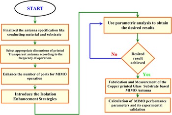
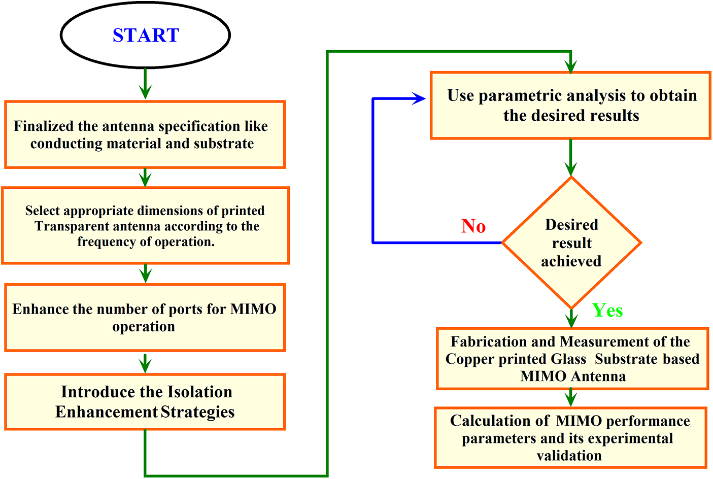
The flowchart for transparent MIMO provides a step-by-step detailing of how one should proceed through the process to design and develop the product by finalizing antenna specifications, like the selection of the conducting material and substrate (c.f Figure 1). The selection of the required dimension for antenna elements according to the target operating frequency has to be selected to enhance optimal performance. To increase the MIMO capabilities of the antenna, the number of ports is increased, and isolation techniques are used to minimize interference between the antenna elements. Parametric analysis is then performed, varying design parameters such as element dimensions, spacing, and feed locations, which allows for fine-tuning of the antenna’s performance. Once optimized, the antenna is fabricated and tested through intense measurements, for example, measuring the channel capacity and bit error rate of a MIMO performance. These are then compared against theoretical predictions for verification purposes of the desired design performance standards. It makes sure the transparent MIMO antenna is produced while satisfying all required specifications and achieving reliable performance in advanced communication applications with full transparency and compact designs that can easily be mounted on aesthetic and multifunctional platforms.
Methodology of the proposed work.
Proposed antenna design
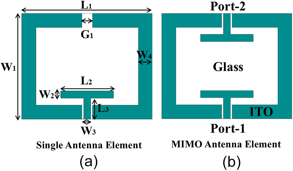
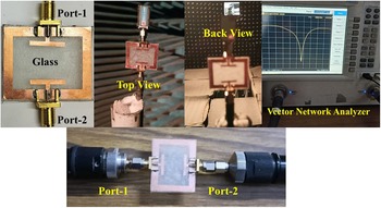
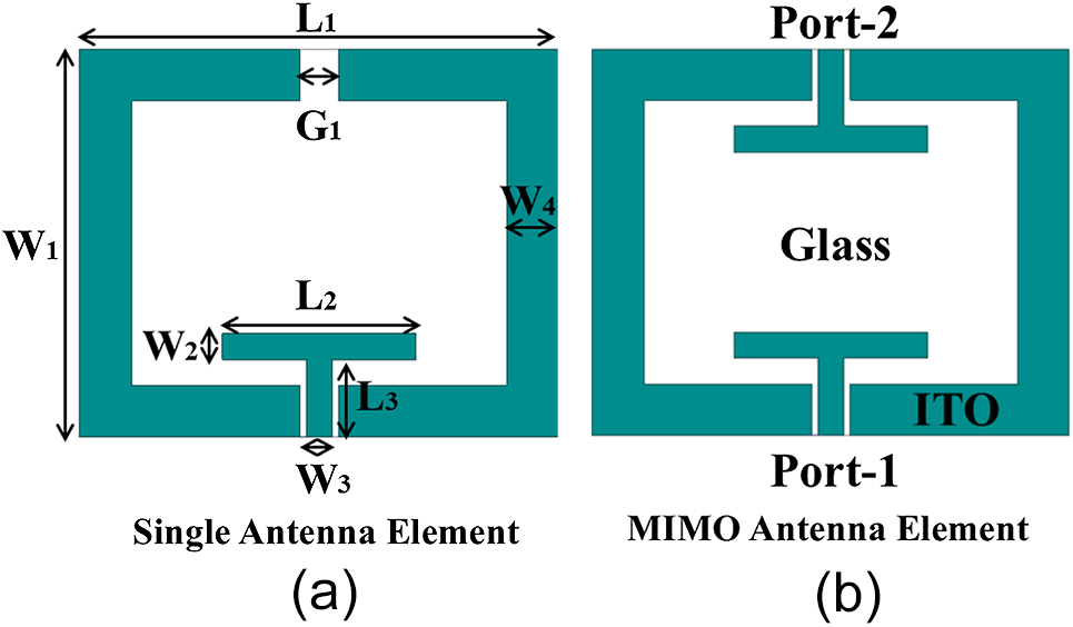
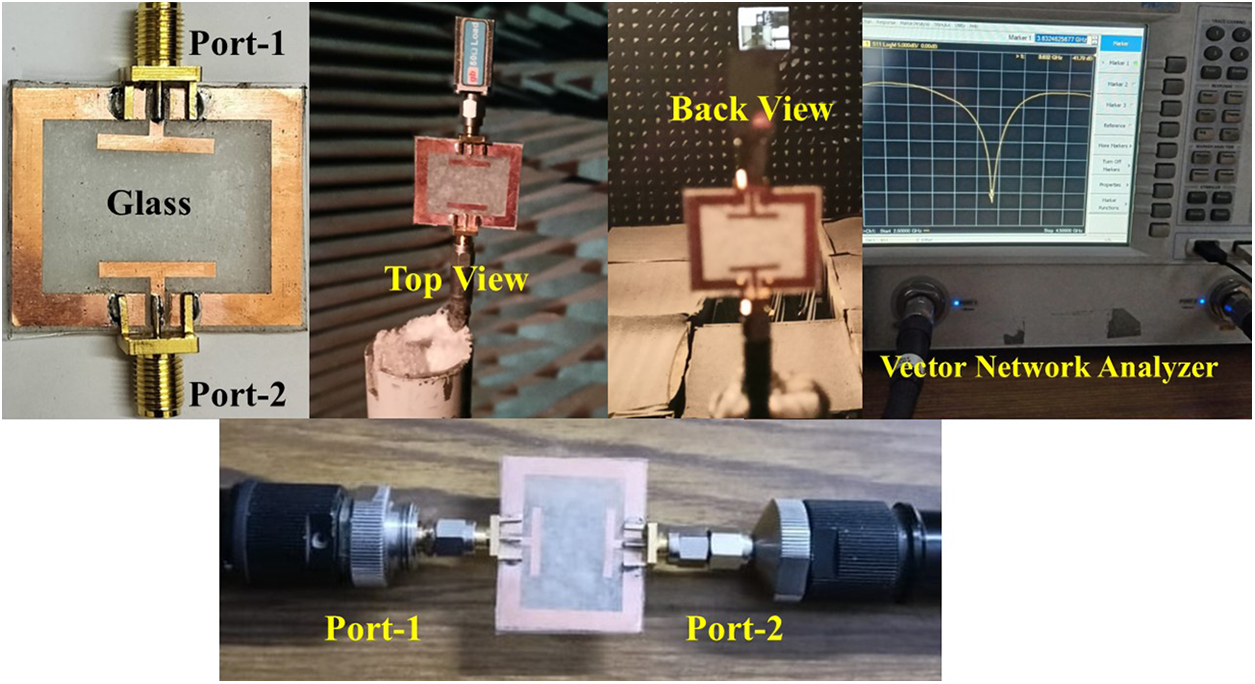
Figure 2(a) and (b) represents the geometrical overview of the proposed single antenna and MIMO antenna model, respectively. Figure 3 represents the fabricated prototype of the proposed MIMO antenna module with a measurement setup. The two-port MIMO antenna shown has two radiating components in the form of a T, placed in opposition to each other and linked by 50 Ω SMA connectors. There is a rectangular ground plane in the shape of a ring and T-shaped radiators that are located on top of the clear glass base. To model and fine-tune the suggested antenna, we use the Ansys HFSS electromagnetic solver.
Geometrical specification of the (a) unit and (b) MIMO element of the proposed antenna.
Fabricated copper-printed glass substrate-based MIMO antenna with measurement setup.
The suggested single antenna measures 37 × 30 × 0.7 mm3 and is affixed to a glass substrate with a relative permittivity of 5.5, ensuring optical transparency for the antenna. The antenna’s radiator is configured in a T-shape, including a rectangular stub connected to a 50-ohm transmission line, with the rear section of the substrate composed of glass. The MIMO antenna arrangement is achieved by mirroring the unit cell along the x-axis while preserving the overall dimensions of 37 × 30 × 0.7 mm3. The geometric parameters of the antenna include L1 = 37 mm (outer loop length, determining the resonant frequency), L2 = 15 mm (horizontal T-stub length, which affects the impedance matching), L3 = 6 mm (vertical T-stub length, which determines the impedance matching), W1 = 30 mm (outer loop width, which determines impedance and bandwidth), W2 = 2 mm (horizontal T-stub width, which affects impedance and bandwidth), W3 = 3 mm (vertical T-stub width, which determines impedance and bandwidth), W4 = 4 mm (inter-element spacing for SRRs, which plays a crucial role in MIMO performance and mutual coupling), G = 3 mm (feed line to SRR gap, which affects impedance matching and circular polarization), and a substrate thickness of 0.7 mm. These parameters are important for optimizing impedance matching, bandwidth, and resonant frequency in the antenna, while the spacing between the SRR elements guarantees circular polarization with proper MIMO functionality as well as minimizes mutual coupling.
Design of a single element antenna
The proposed antenna design uses a split-ring resonator (SRR) structure, and it acts as a single antenna element when only one port, Port-1 or Port-2, is employed, as shown in Fig. 2(a). The resonant frequency of each SRR element is determined mainly by the outer loop dimensions L1 and W1, with fine-tuning achieved through the inner T-shaped matching stubs L2, L3, W2, and W3. The T-shaped stub functions as an impedance transformer, well matching the SRR’s high impedance to that of the 50-ohm feed line impedance for maximal power transfer. The design achieves a circularly polarized radiation pattern in which the electric field vector rotates in circular motion as it propagates down the wave; hence, consistent polarization is always obtained regardless of the antenna orientation. The circular polarization ensures that the signal reception is improved in dynamic environments, reducing the risk of polarization mismatch in various wireless communication applications. Furthermore, the SRR design supports miniaturization, making the antenna compact and suitable for integration into systems where space is limited. The performance of the structure, combined with ease of impedance matching and efficient radiation characteristics.
Design of MIMO antenna
When both Port-1 and Port-2 are excited simultaneously, the antenna acts as a two-port MIMO system, as shown in Fig. 2(b). The spatial diversity is given by placing the two ports in front-to-front orientation. This spatial separation allows the signals transmitted or received by each antenna element to follow different propagation paths, which reduces the chances of multipath fading and improves the overall link reliability and data rates. An important parameter in MIMO design is the correlation between the antenna elements, and generally, the lower the correlation, the better the MIMO performance, with higher diversity and improved system capacity. The spacing W4 and the design of the SRRs also affect this correlation, such that a greater spacing usually means a lower correlation and, hence, better performance for the MIMO system. Still, mutual coupling between the two elements is unavoidable. Mutual coupling arises from the fact that the current in one element causes a voltage in the other, which could degrade the performance and efficiency of the antenna. This mutual coupling needs to be minimized to ensure optimal MIMO performance because it degrades the antenna’s ability to distinguish between different signal paths, affecting the data throughput and overall system reliability. These issues can be addressed by carefully optimizing element spacing and SRR design to improve the antenna’s efficiency in a MIMO configuration for high-capacity wireless communication.
Antenna design evolution stages
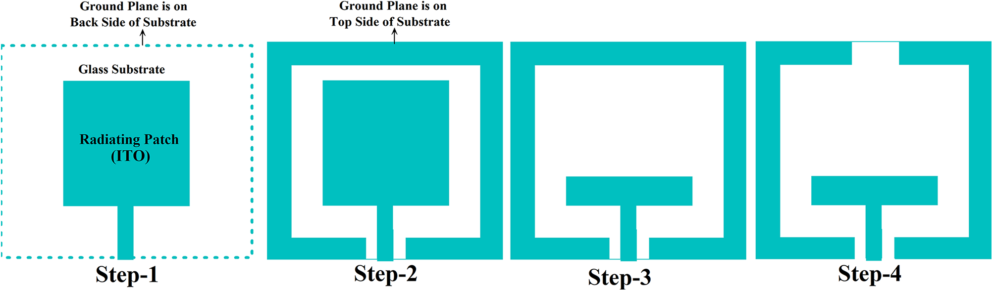
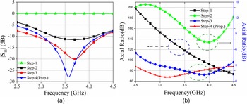
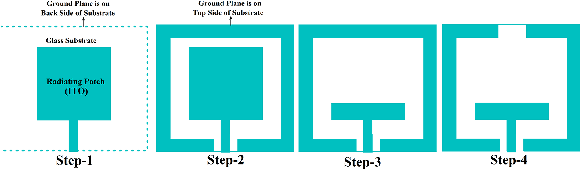
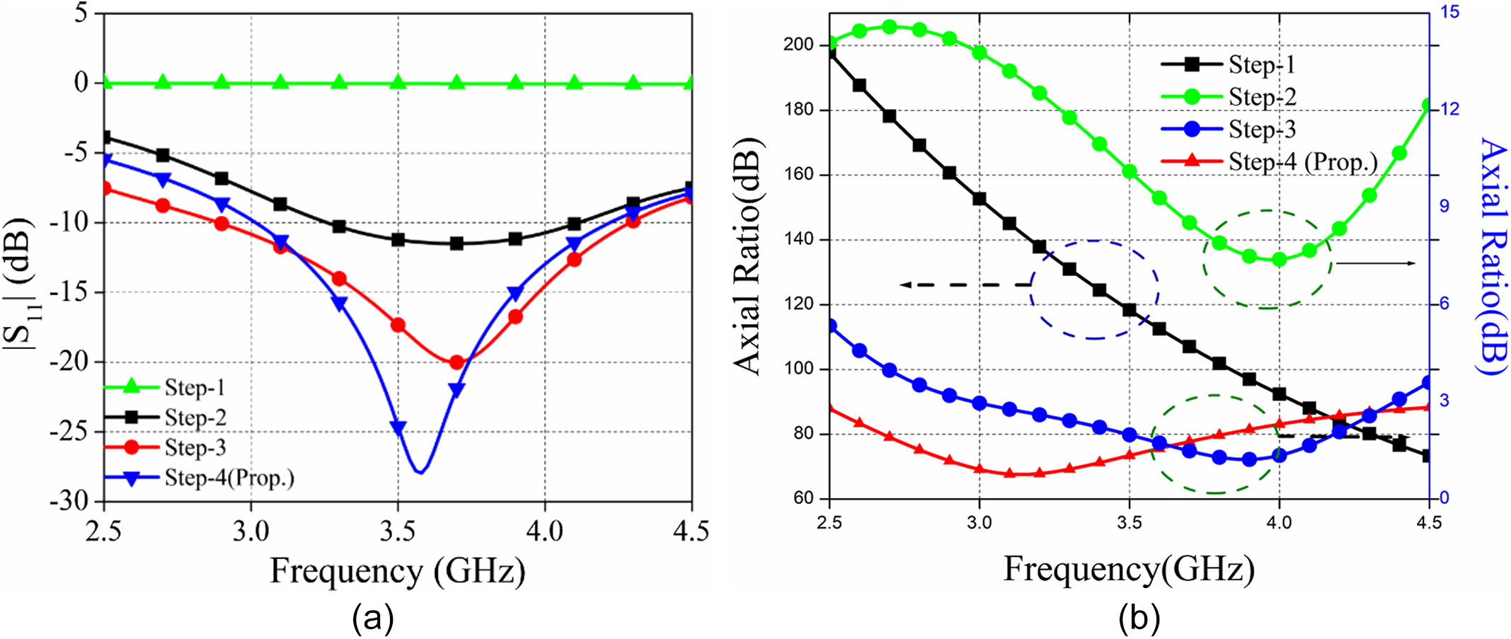
The suggested single antenna element has undergone four distinct phases (see Fig. 4), each designed to enhance performance regarding |S11| (dB) and axial ratio (dB), as seen in Fig. 5(a) and (b), respectively. In Step 1, a fully grounded basic rectangular patch antenna with a microstrip feed line is introduced. This antenna is linearly polarized, with the electric field oriented along the length of the patch. In Step 2, the same rectangular patch antenna is designed with a ground plane that is shifted on the same side of the patch and converted into a square ring configuration to increase impedance bandwidth, resulting in a single resonance at 3.7 GHz and achieving circular polarization (CP). Step 3 involves reshaping the rectangular radiator into a T-shaped one, which increases the impedance bandwidth and changes the resonance to 3.8 GHz. An Axial Ratio Bandwidth (ARBW) of 1 GHz is achieved by this design. Step 4 involves making further adjustments to the antenna design to meet the goals of the stated axial ratio bandwidth and impedance bandwidth for N77/78 applications. By carefully inserting the rectangular slot into the square ring ground plane, the design from Step 4 is able to accomplish a 100% 3-dB impedance bandwidth, which includes the necessary 5G NR Bands n77 and n78. Incorporating a rectangular hole into the radiator, which originated in Step 3, increases the maximum impedance bandwidth to 3–4.3 GHz and the 3-dB axial ratio bandwidth to 2.5–4.5 GHz. This design is suitable for 5G NR applications since it shows improved performance across the defined frequency ranges.
Evolution of the suggested single antenna element.
(a) |S11| and (b) axial ratio plot for antenna development phases.
Parametric investigation
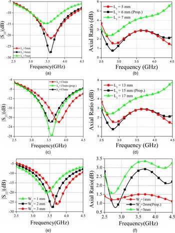
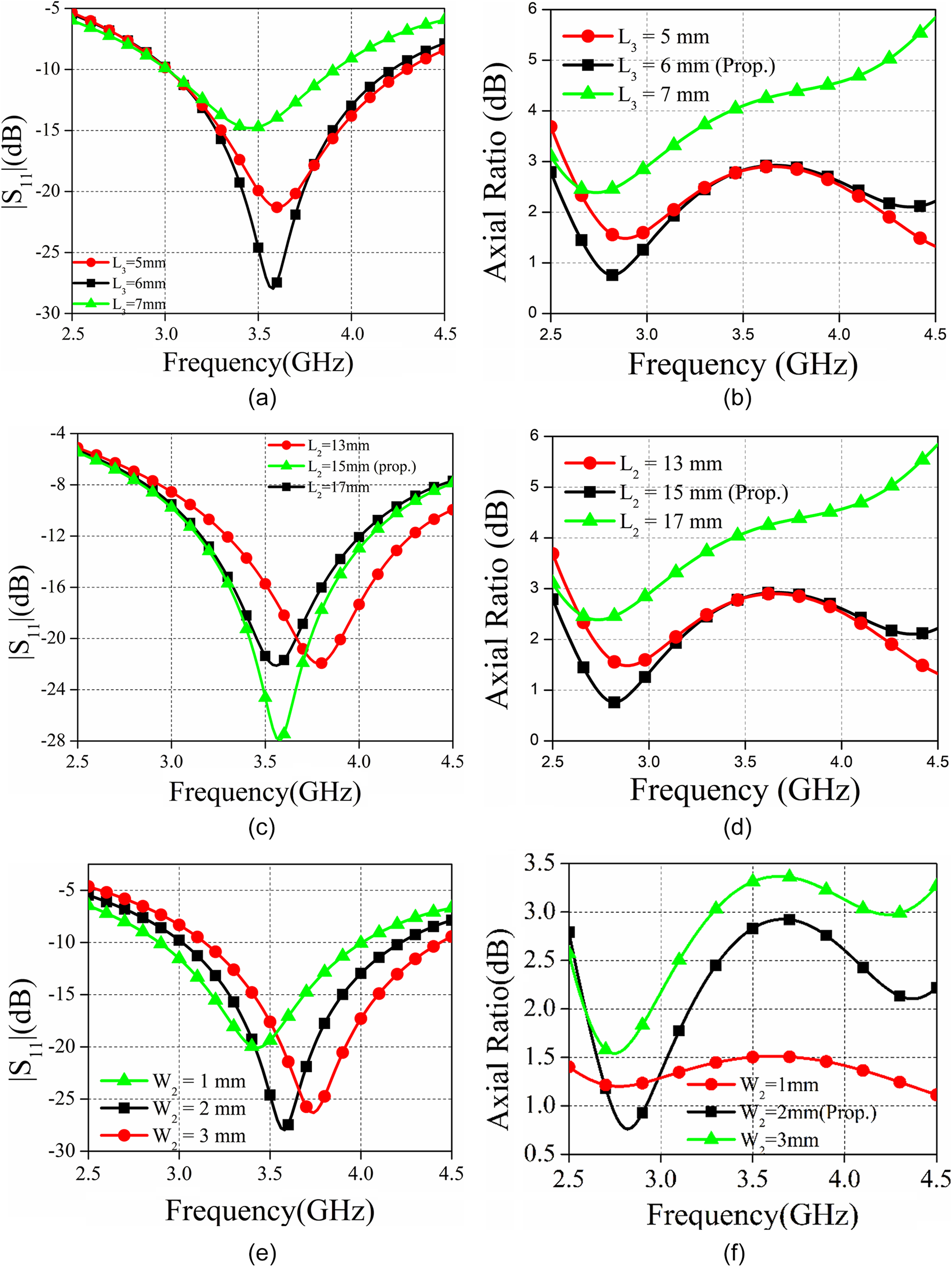
To learn how important design elements like feed length (L3), radiator length (L2), and radiator width (W2) affect the proposed antenna’s impedance bandwidth and axial ratio bandwidth (ARBW), parametric research is conducted. The impedance bandwidth and ARBW are both significantly impacted by L3. For L3 “1” mm step analysis has been conducted, from the perusal of Fig. 6(a) and (b) it is clear that the minimum value of return loss and 100% ARBW is achieved for L3 = 6 mm. For L2, the analysis has been completed for three different values of 13, 15, and 17 mm. From Fig. 6(c) and (d) it is clear that the minimum value of return loss and 100% ARBW is achieved for L2 = 17 mm. Similar behavior is also observed for the width of the feed line, for three different variations of W2, the final value of W2 = 2 mm is finalized, where the minimum value of return loss with 100% ARBW is attained (see Fig. 6(e) and (f)).
Parametric analysis in terms of |S11| and AR for different values of (a) L3 (|S11|), (b) L3 (AR), (c) L2 (|S11|), (d) L3 (AR), (e) W2 (|S11|), and (f) W2 (AR).
Mechanism for CP generation
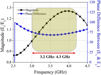
Figure 5b shows that the suggested design achieves a 100% 3-dB (ARBW) over the whole range of operation. A graph is shown to clarify the circular polarization characteristics of the two-port MIMO prototype. The graph shows the ratio of the magnitudes of the two electric field components (EX/Ey) and the phase difference (EX − Ey) between these components throughout the relevant frequency region (see Fig. 7). The engineered antenna exhibits an extensive circular polarization bandwidth, shown by an impedance bandwidth of 3.0–4.3 GHz, demonstrating a field component ratio of around 1 and a phase difference ranging from 70° to 80°.
The magnitude and phase difference plots of electric field vectors (EX/Ey).
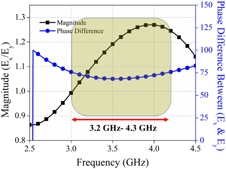
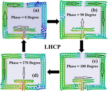
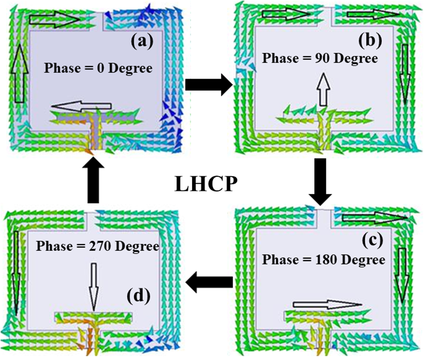
Figure 8 illustrates the distribution of surface current for a single antenna element in the two-port design. The handedness of the circularly polarized wave is seen here. The current distribution graph is shown for various theta values (0°, 90°, 180°, and 270°) at the resonant frequency of 3.7 GHz. The existence of left-handed circular polarization (LHCP) waves is signified when the surface currents on the rectangular ground plane and the T-shaped antenna radiator rotate clockwise at distinct phase angles [Reference Dwivedi, Sharma, Singh and Singh23].
Generating CP waves of the proposed antenna with (a) phase angle of 0°, (b) phase angle of 90°, (c) phase angle of 180°, and (d) phase angle of 270°.
Results and discussion
In this section, two cases are discussed as follows.
Case 1: Comparative analysis between ITO-printed MIMO antenna and copper-printed MIMO antenna
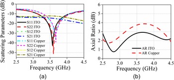
The scattering parameter graphs for the ITO and copper-printed MIMO antenna have been presented in Fig. 9. The electrical conductivity of ITO is in the order of 105 while for copper sheet it is in the order of 108. By careful observation of the plot in Fig. 9(a), it is clear that for the copper-printed antenna, the resonance frequency is shifted to a higher frequency region from 3.6 to 3.67 GHz, and the isolation between the antenna elements decreases from 15 to 13 dB. These marginal variations in the scattering characteristics are due to the higher electrical conductivity of copper as compared to the ITO sheet. From Fig. 9(b), it is observed that for the ITO-printed sheet, the axial ratio is less than 3 dB for the whole operating bandwidth, while for the copper-printed sheet, the axial ratio is less than 4 dB. Both characteristics validate the circular polarization attributes for the proposed MIMO antennas.
(a) Scattering parameters and (b) axial ratio of ITO and copper-based MIMO antenna.
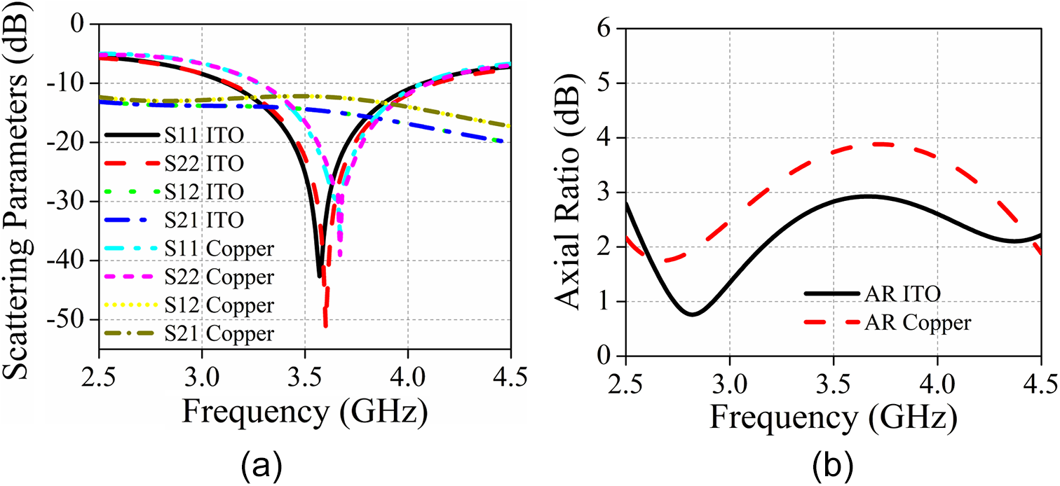
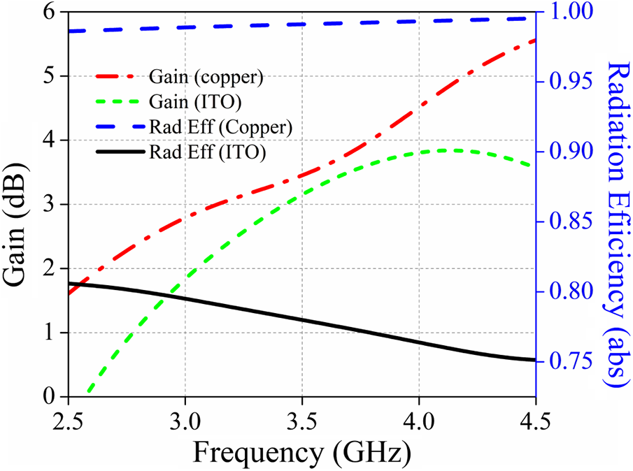
Figure 10 represents the comparative plots in terms of gain and radiation efficiency for both the ITO- and copper-printed sheets. From the perusal of Fig. 10, it is observed that the gain and radiation efficiency for copper-based clad is better compared to ITO-based transparent clad sheet. The radiation efficiency for the ITO-printed antenna is 75% while for copper it is 99% and the peak gain for the ITO sheet is 3.9 dB, while for copper it is 4.8 dB.
Gain and radiation efficiency graph for both ITO- and copper-printed MIMO antenna.
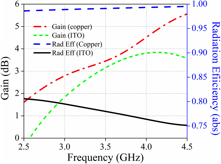
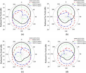
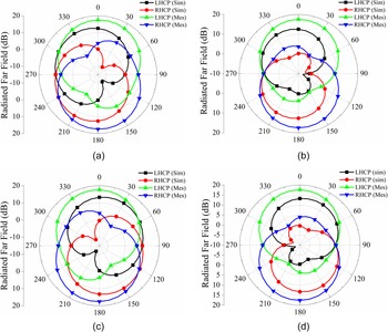
Figure 11 represents the LHCP/RHCP plots for Port-1 and Port-2 for both the ITO-based MIMO antenna and copper-based MIMO antenna. From Fig. 11, it is clear that for both cases, the proposed MIMO module is LHCP for both ports. The separation between the LHCP and RHCP radiation patterns in ITO-based MIMO antennas is notably superior when compared to copper-based MIMO antennas.
LHCP/RHCP plots for Port-1 and Port-2 for both ITO-based MIMO antennas in (a) Port-1 XoZ plane, (b) Port-1 YoZ plane, (c) Port-2 XoZ plane, and (d) Port-2 YoZ plane.
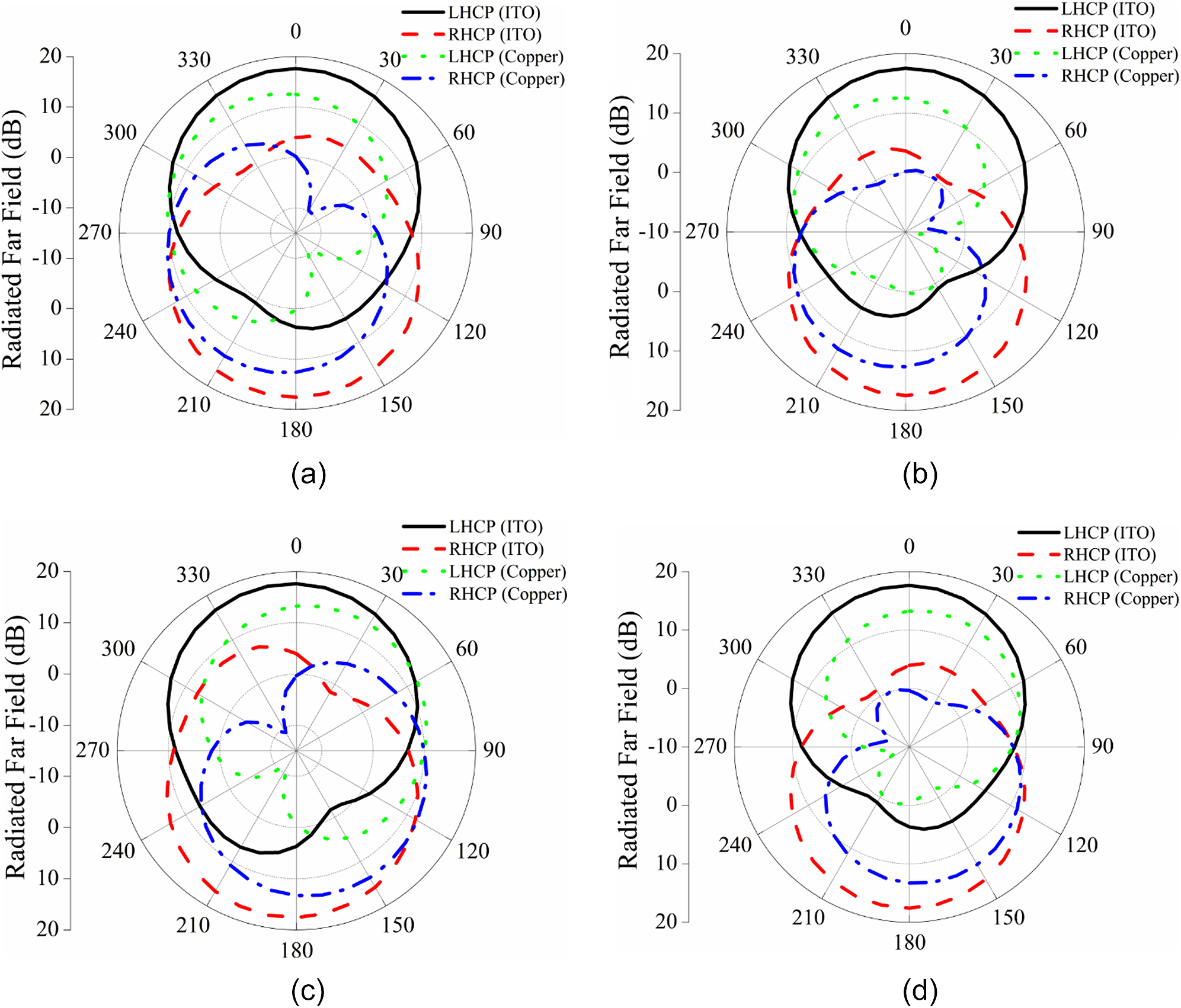
From this aforementioned comparative analysis between the ITO-based transparent MIMO antenna and copper-based MIMO antenna, it can be concluded that the findings of both configurations are almost the same for the proposed MIMO antenna design, and both are well suited for N77 (3.3–4.2 GHz)/78 (3.3–3.8 GHz) fifth-generation frequency band application
Case 2: Experimental results of the fabricated copper-based MIMO antenna
To validate the simulated findings of the proposed MIMO antenna, a fabricated model has been created. The fabricated design consists of a copper sheet as the conducting sheet and glass as a substrate, as shown in Fig. 3. The measurement of the design model has been carried out with the help of a vector network analyzer in an anechoic chamber and an open environment.
Scattering parameters and gain attributes
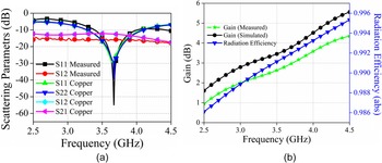
Figure 12(a) illustrates the comparison between the simulated and measured mutual coupling (S21 and S12), specifically focusing on the return losses of the two ports (S11 and S22) alongside the different antenna units. Figure 12(b) demonstrates that the simulated and observed scattering results are consistent, with minor errors that may be rectified by appropriate manufacturing and measurement techniques. The suggested MIMO design has an impedance bandwidth of |S11| <−10 dB, spanning from 3.2 to 4.3 GHz in simulations and 3.3 to 4.35 GHz in measurements, with isolation of |S12| <−15 dB. Figure 12(b) illustrates the graph of the simulated radiation efficiency and the observed and simulated gain (dB). Gains of 2 to 4 dB were computed or observed for the specified resonating bandwidth of 3.3–4.35 GHz. The observed and simulated gains correspond closely, with the little variation attributed to the physical limitations encountered during the antenna’s measurement and fabrication. The two-port MIMO antenna has a radiation efficiency over 98% in the 3.3–4.35 GHz frequency band.
The simulated/measured (a) scattering parameters and (b) gain and simulated radiation efficiency.
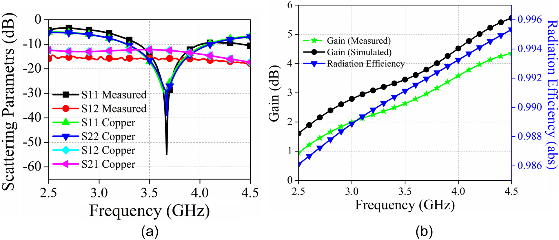
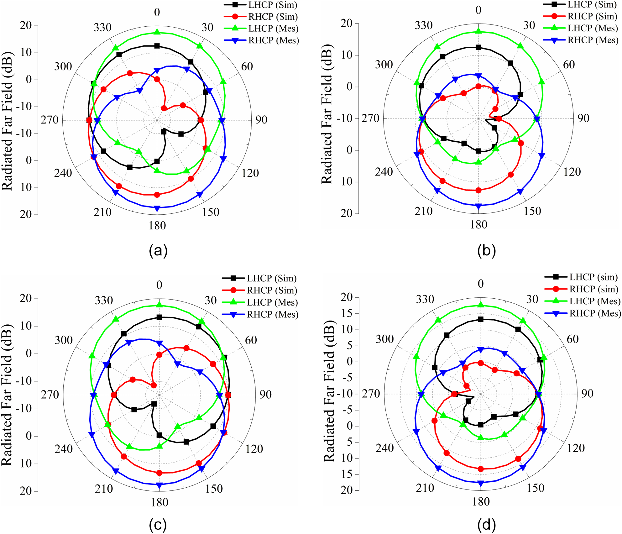
Figure 13(a) and (b) present the simulated and measured outcomes of the two-dimensional radiation patterns in the XoZ-plane (ϕ = 0°) and YoZ-plane (ϕ = 90°) for the proposed MIMO antenna. The proposed antenna exhibits a left-handed circular polarization (LHCP) pattern at both ports in the broadside direction, as illustrated in Fig. 12 shows that the proposed antenna has a broadside left-handed circular polarization (LHCP) pattern at both ports. By isolating the LHCP and RHCP patterns in both main planes by more than 15 dB, this antenna design demonstrates remarkable cross-polarization discrimination (XPD). The circular polarization properties of the provided two-port MIMO antenna are further confirmed by the emission patterns.
LHCP/RHCP plots for (a) Port-1 XoZ, (b) Port-1 YoZ, (c) Port-2 XoZ, and (d) Port-2 YoZ.
Diversity parameters
To validate the design of a two-port MIMO antenna and assess the performance of the MIMO system, optimal values for parameters including ECC, DG, CCL, and MEGs are determined. ECC offers a measure of correlation to analyze the impact of radiation patterns on the related antenna components. The industrial standard specification indicates that the range of ECC should be maintained below 0.Reference Liang, Gao, Cheng, Jiang, Dai, Zhang, Cheng, Jin and Cui5 to ensure optimal performance of the MIMO antenna [Reference Sharawi24]. The literature indicates that there are two techniques for estimating the value of ECC. The initial method utilizes scattering characteristics to derive the ECC value (Reference Kocia and HumEq. 1), whereas the subsequent method leverages far-field radiation patterns to ascertain the ECC value (Reference An, Xiong, Xu, Yang, Fu and MaEq. 2). The initial approach for calculating ECC is applicable when the radiation efficiency of the proposed MIMO antenna exceeds 90%.
 \begin{equation}{\rho _{eij}} = \frac{{{{\left| {{S_{ii*}}{S_{ij}} + {S_{ji*}}{S_{jj}}} \right|}^2}}}{{\left( {1 - {{\left| {{S_{ii}}} \right|}^2} - {{\left| {{S_{ij}}} \right|}^2}} \right)\left( {1 - {{\left| {{S_{ji}}} \right|}^2} - {{\left| {{S_{jj}}} \right|}^2}} \right)}}\end{equation}
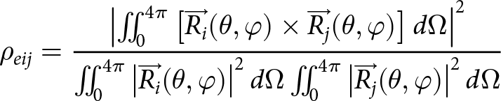 \begin{equation}
\rho_{eij}=\frac{\left|\iint^{4\pi}_{0}\left[\overrightarrow{R_{i}}(\theta, \varphi)\times\overrightarrow{R_{j}}(\theta, \varphi)\right]d{\Omega}\right|^{2}}{\iint^{4\pi}_{0}\left|\overrightarrow{R_{i}}(\theta, \varphi)\right|^{2}d{\Omega}\iint^{4\pi}_{0}\left|\overrightarrow{R_{j}}(\theta, \varphi)\right|^{2}d{\Omega}}\end{equation}
The transmission coefficient is Sij, whereas the reflection coefficient is Sii. The three-dimensional radiation values of the ith and jth antennas are designated as 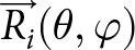 $\overrightarrow{R_{i}}(\theta, \varphi)$ and
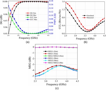
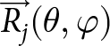 $\overrightarrow{R_{j}}(\theta, \varphi)$. We use Ω to denote solid angles. Figure 14(a) shows that the proposed two-port MIMO antenna’s ECC is less than 0.001 for the operational impedance bandwidth for both simulated and measured.
Diversity parameters of the proposed MIMO antenna: (a) ECC & DG, (b) CCL, and (c) MEG.
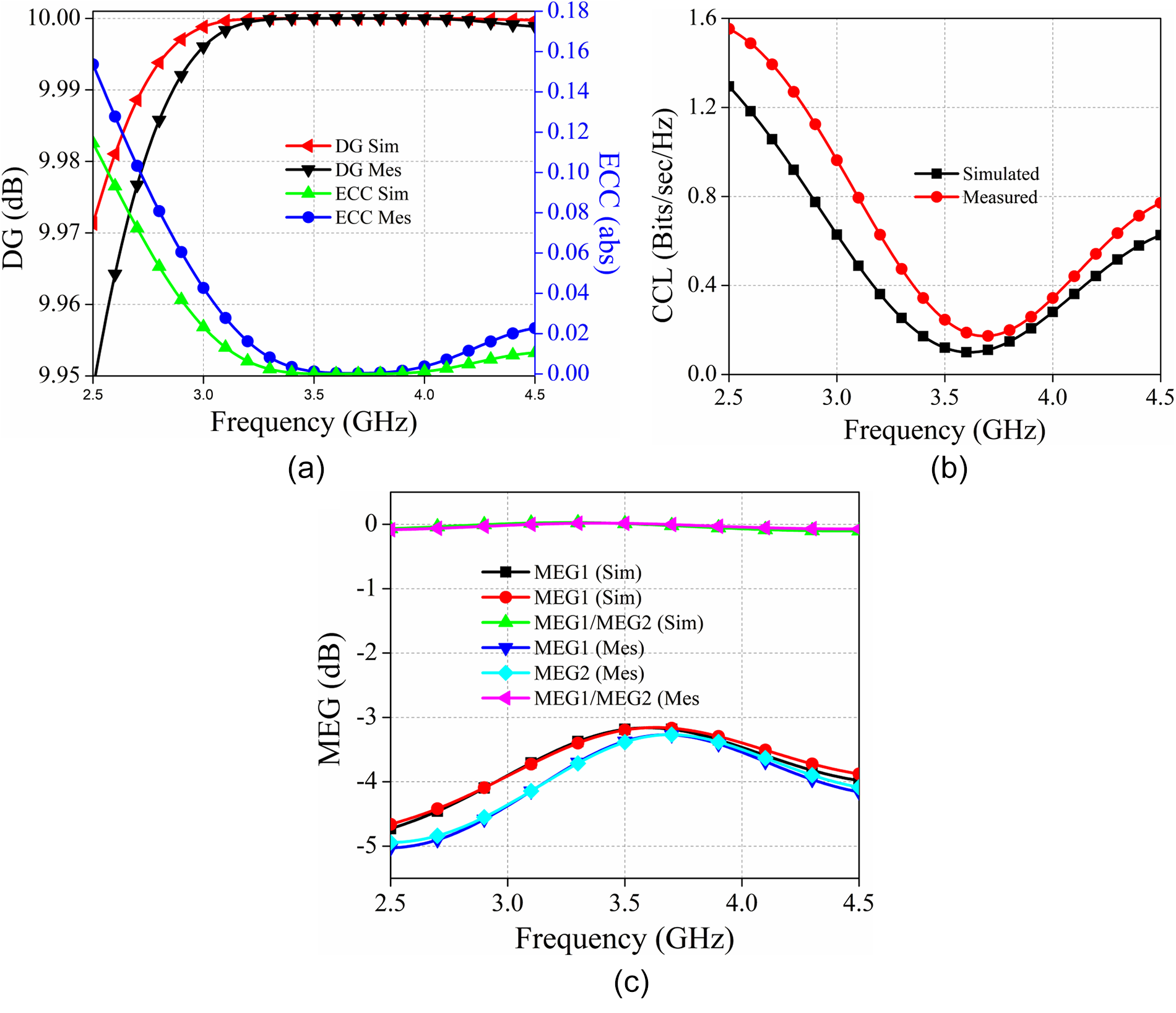
The diversity gain (DG) refers to a decrease in transmission power or an enhancement in diversity performance, as indicated by the signal-to-noise ratio (SNR), following the application of the diversity scheme. By utilizing Eq. (3), one can determine the directivity gain of a MIMO antenna; an optimal directivity gain value is approximately 10 dB for enhanced performance. The performance of the proposed antenna in terms of diversity for MIMO applications is confirmed by its DG value, which exceeds 9.99 dB (see Fig. 14(a)).
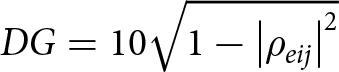 \begin{equation}DG = 10\sqrt {1 - {{\left| {{\rho _{eij}}} \right|}^2}} \end{equation}
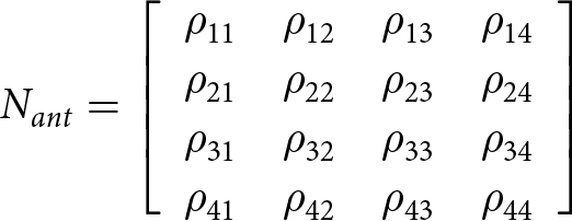
The maximum amount of channel loss that allows a message to be efficiently sent across a communication channel may be predicted quantitatively using the Channel Capacity Loss metric. Reliable communication requires that the CCL not exceed 0.4 bits per second per GHz. Equation (4) contains the formula for calculating the CCL.
 \begin{equation}CCL = - {\log _2}det\left| {{N_{ant}}} \right|\end{equation}
 \begin{equation}{N_{ant}} = \left[ {\begin{array}{*{20}{c}}
{{\rho _{11}}}&{{\rho _{12}}}&{{\rho _{13}}}&{{\rho _{14}}} \\
{{\rho _{21}}}&{{\rho _{22}}}&{{\rho _{23}}}&{{\rho _{24}}} \\
{{\rho _{31}}}&{{\rho _{32}}}&{{\rho _{33}}}&{{\rho _{34}}} \\
{{\rho _{41}}}&{{\rho _{42}}}&{{\rho _{43}}}&{{\rho _{44}}}
\end{array}} \right]\end{equation}
The calculated and observed CCL values for the suggested frequency bandwidth, which is less than 0.30 bits/sec/Hz, are shown in Fig. 14(b).
The Mean Effective Gain (MEG) serves as a crucial diversity metric, evaluating the received power of a MIMO antenna in relation to that of an isotropic antenna. A MIMO antenna performs optimally when the MEG1/MEG2 ratio is maintained below 3 dB [Reference Narayanaswamy, Satheesha, Alzahrani, Pandey, Dwivedi, Singh and Tolani25]. The values of the MEG can be determined using Eqs. Reference Sheikh, Shokooh‐Saremi and Bagheri‐Mohagheghi(6) and (7).
Figure 14(c) shows MEG1, MEG2, and MEG1/MEG2 data for the proposed radiator. The MEG1/MEG2 ratio is around 0 dB.
 \begin{equation}ME{G_1} = 0.5[1 - {\left| {{S_{11}}} \right|^2} - {\left| {{S_{12}}} \right|^2}]\end{equation}
 \begin{equation}ME{G_2} = 0.5\left[ {1 - {{\left| {{S_{12}}} \right|}^2} - {{\left| {{S_{22}}} \right|}^2}} \right]\end{equation}
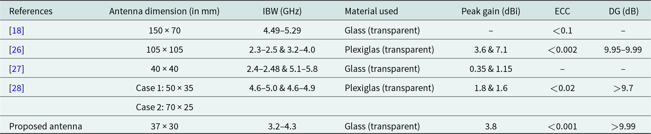
Table 1 has been created to enable a comparative analysis of the efficacy of our MIMO antenna against other relevant studies. The table indicates that, in comparison to the other antennas evaluated for wave applications, the proposed antenna demonstrates superior performance due to its compact size, broad operational range, and high gain. In comparison to other MIMO radiators operating within the same frequency range, the two-port MIMO antenna demonstrates superior performance, as illustrated in Table 1.
The comparative investigation of the proposed two-port MIMO antenna with other two-port MIMO antennas
Conclusion
The article details the steps used to create and validate an ITO-based optically transparent multiple-input multiple-output antenna. Transparency is provided by glass substrates, while the base and built-in radiating element are composed of copper. At its center frequency of 3.6 GHz, the ITO-based antenna displays circular polarization with a peak return loss of 28 dB and a gain of less than 3 dB. The constructed reflect array has a bandwidth of 20% and a total optical transparency of 75%. The optically transparent reflect array’s large phase range, high optical transparency, low return loss, and broad bandwidth make it an attractive candidate for use with ITO materials in high-performance OTRAs. This paper presents a proposed antenna featuring an ITO structure designed to address current optical and electrical limitations. We have designed and simulated the transparent antenna using ITO, while fabricating it with copper to maintain all significant parameters, due to the unavailability of the necessary techniques for fabrication with ITO.
Funding statement
No funds, grants, or other support were received.
Competing interests
There are no potential conflicts of interest.
Ethics approval and consent to participate
Not applicable.

Smitha D was born in the Chikkaballapura district in 2003. She completed her Bachelor’s in Electronics and Communication Engineering from Nagarjuna College of Engineering and Technology, Bengaluru, in 2025. She is currently working at iOPEX Technologies in the field of networks and security. Her research interests include microwave and antenna propagation, machine learning, VLSI design, and advanced networking.

Nayana BR was born in Devanahalli, Bengaluru, Karnataka, in the year 2003. She has completed her bachelor’s in the year 2025 from Nagarjuna College of Engineering and Technology, Bengaluru, in Electronics and Communication Engineering. Her research interests include microwave and antenna propagation, machine learning, VLSI design, and advanced networking.

Pramukhya MM was born in Chikmagalur in the year 2003. She has completed her bachelor’s in the year 2025 from Nagarjuna College of Engineering and Technology, Bengaluru, in Electronics and Communication Engineering. Her research interest lies in communication technology, machine learning techniques for image enhancement and medical image processing. She has collaborated actively with researchers in several disciplines of research interest.

Brunda M was born in the Chikkaballapura district of Karnataka in the year 2003. She has completed her bachelor’s in the year 2025 from Nagarjuna College of Engineering and Technology, Bengaluru, in Electronics and Communication Engineering. Her research interests include microwave and antenna propagation, machine learning, VLSI design, and advanced networking.

Dr. Ajay Kumar Dwivedi (senior member, IEEE; https://orcid.org/0000-0003-1146-0902) is an Associate Professor and Research Head in the Department of Electronics and Communication Engineering at Cambridge Institute of Technology, K. R. Puram, Bangalore, India. He received his B.Tech. in Electronics and Communication Engineering from Uttar Pradesh Technical University, Lucknow, in 2010, M.Tech. in Wireless Communication from Sam Higginbottom University of Agriculture, Technology and Sciences, Allahabad, in 2015, and Ph.D. in Electronics and Communication Engineering from the Indian Institute of Information Technology Allahabad, Prayagraj, India, in 2021. With over 15 years of academic and research experience, Dr. Dwivedi has authored and co-authored more than 100 research papers in reputed international and national journals and conference proceedings. His primary research interests include RF and microwave engineering, dielectric resonator antennas (DRA), MIMO antenna systems, metamaterial-based antenna design, and next-generation wireless communication technologies (5G/6G). He has made notable contributions to the design and optimization of advanced antenna systems and has been actively involved in funded research projects and collaborative initiatives. Dr. Dwivedi holds professional memberships as a Life Member of IETE, ISTE, and IAENG, and he is an active member of the IEEE Antennas and Propagation Society and the IEEE Microwave Theory and Technology Society. He also serves as a reviewer for high-impact journals, including IEEE Transactions on Vehicular Technology, IEEE Sensors Letters, IEEE Internet of Things Journal, Wireless Personal Communications, Computer Networks, and Journal of Infrared, Millimeter and Terahertz Waves. In recognition of his expertise, Dr. Dwivedi is an Editorial Board Member of Scientific Reports, Nature and an Academic Editor of International Transactions on Electrical Energy Systems, Wiley.

Dr. Vivek Singh (https://orcid.org/0000-0001-7569-0104) is working as an Associate Professor in the Department of Electronics and Communication Engineering at Cambridge Institute of Technology, K. R. Puram, Bangalore, India. He completed his Ph.D. degree in 2019 and M.Tech. degree in 2012 from the Department of Electronics and Communication Engineering at the University of Allahabad (Central University), U.P., India. He completed his B.Tech. in Electronics and Communication Engineering from Uttar Pradesh Technical University, Lucknow, India, in 2009. He is a member of IEEE, a fellow member of IETE, and various other societies such as the Antennas Wave and Propagation Society. He has been in the academic and research fields for more than 14 years and has guided many UG, PG, and PhD students. He has authored or co-authored more than 80 research papers in international journal/conference proceedings. His research interests include printed antennas, dielectric resonator antennas, MIMO antennas, metamaterial-based antennas, and RF Communication systems. He is a reviewer of many Web of Science/Scopus-indexed journals and international conference proceedings.