I. INTRODUCTION
Both the fields of photovoltaics and photoelectrochemistry have sought to exploit nanostructured, high-aspect ratio forms of GaAs, GaP, and InP as efficient photoelectrode platforms. Reference Hu, Chi, Fountaine, Yao, Atwater, Dapkus, Lewis and Zhou1–Reference Wallentin, Anttu, Asoli, Huffman, Aberg, Magnusson, Siefer, Fuss-Kailuweit, Dimroth, Witzigmann, Xu, Samuelson, Deppert and Borgstrom4 These classic III-V materials can exhibit excellent optoelectronic properties (i.e., optimal band gaps, high-charge carrier mobilities, and ability to be doped precisely) that are critical for efficient charge generation and separation. However, the prospects for constructing photoelectrochemical technologies at a globally relevant scale based solely on these materials are complicated by the relative scarcity and high cost of Ga and In. Reference Woodhouse, Goodrich, Margolis, James, Lokanc and Eggert5 Accordingly, there is a pressing need and opportunity for materials with similarly favorable properties, but which are composed of only earth abundant elements. Reference Woodhouse, Goodrich, Margolis, James, Lokanc and Eggert5,Reference Lewis and Nocera6
Ternary II-IV-V2 chalcopyrite semiconductors are one class of semiconductors that are potentially ideal for photoelectrochemical technologies. Specifically, zinc-based phosphides (Zn–IV–P2; IV = Ge, Sn, or Si) have been identified as analogs and low-cost alternatives to the aforementioned class of III-V semiconductors. Reference Collins, Hankett, Carim and Maldonado7–Reference Yokoyama, Oba, Seko, Hayashi, Nose and Tanaka9 These semiconductors both are comprised of naturally abundant elements and are isoelectronic with the III-V semiconductors. Moreover, the respective band structures are remarkably similar, resulting in nearly identical band gap energies and the possibility of high-charge carrier mobilities. Reference Gashimzade10,Reference Shay and Wernick11
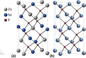
In this report, we focus on ZnSnP2. ZnSnP2 is isoelectronic with InP and can exhibit either chalcopyrite or sphalerite crystal structure (Fig. 1). For ZnSnP2, the optoelectronic band gap energy is a function of the crystalline phase. The chalcopyrite phase of ZnSnP2 has a band gap of 1.68–1.75 eV, and the sphalerite phase of ZnSnP2 has a smaller band gap energy between 1.22 and 1.38 eV. Reference St-Jean, Seryogin and Francoeur12 In either phase, ZnSnP2 natively exhibits p-type conductivity with the capacity for good majority carrier mobilities (10–70 cm2 V−1 s−1), Reference Shay and Wernick11,Reference Davis and Wolfe13 thus rendering ZnSnP2 amenable for solar energy capture/conversion. Reference St-Jean, Seryogin and Francoeur12,Reference Ryan, Peterson, Williamson, Frey, Maciel and Parkinson14,Reference Scanlon and Walsh15
ZnSnP2 unit cell with either (a) cation-ordered chalcopyrite crystal structure or (b) cation-disordered sphalerite crystal structure. Note for (b), the Zn and Sn atoms have 0.5 probability of occupying the cation sites, and the resulting unit cell is cubic Zn0.5Sn0.5P, i.e., two unit cells are shown in (b).

To date, the preparation of single-phase ZnSnP2 crystals has proven challenging. Based on the pseudo-binary Sn–ZnP2 phase diagram, ZnSnP2 melts incongruently and forms peritectically. Reference Shay and Wernick11,Reference Borshchevskii and Vysotina16 Thus far, ZnSnP2 bulk crystals have been synthesized from melts, Reference Davis and Wolfe13,Reference Borshchevskii and Vysotina16,Reference Mughal, Payne and Ray17,Reference Rubenstein and Ure18 vapor phase deposition, Reference Ajmera, Shin and Zamanian19,Reference Sansregret20,Reference Seryogin, Nikishin, Temkin, Mintairov, Merz and Holtz21 and organometallic synthesis. Reference Goel, Buhro, Adolphi and Conradi22 The occurrence of impurity phases, such as Sn3P2, Sn4P3, and Zn3P2 in as-prepared ZnSnP2, has stymied practical interest.
ZnSnP2 has never been prepared with high-aspect ratio form factors, e.g., nanowires. The objective of this report is to demonstrate the possibility of preparing pure-phase ZnSnP2 in nanostructured form. We demonstrate a benign, simple chemical vapor deposition method that does not involve the use of metal organic or toxic gaseous precursors (e.g., PH3). Instead, we used powdered Zn and SnP3 as the sublimation sources for the growth of ZnSnP2 nanowires via a vapor–liquid–solid (VLS) mechanism through the action of Sn nanoparticle catalysts. Raman scattering, powder x-ray diffraction patterns (XRD), and high-resolution transmission electron microscopy (HRTEM) are presented to illustrate the purity and crystallinity of the materials prepared by the used approach. Preliminary photoelectrochemical measurements are also shown that speak to the conductivity type of the as-prepared materials.
II. EXPERIMENTAL SECTION
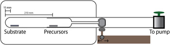
Nanowire growth setup ZnSnP2 nanowires were prepared in custom-built quartz tube in a single-zone furnace (MTI Corporation, GSL-1100X-S) as illustrated in Fig. 2. Zn powder (J.T. Baker, 98.0%) and SnP3 powder [prepared by high-energy ball milling Sn powder (Strem, 99.5%) and red P (Alfa Aesar, 99.999%) in inert environment in a Spex 8000 laboratory shaker mill for 4 h] were used as the precursors for Zn and P, respectively, in the growth process. Zn and SnP3 powders in stoichiometric ratio were loaded into a customized quartz precursor holder (21 mm diameter × 250 mm in length) with a piece of iron enclosed on the other end for a contactless introduction of precursor powders with a magnetic sliding mechanism. When the holder was loaded with the powders, it was placed in a long quartz tube (25 mm diameter × 825 mm in length) that had two growth substrates (total area: 40 mm2) placed on the sealed end. Initially, the holder was left outside of the furnace to prevent premature sublimation of precursor powders. The assembly was then evacuated with a mechanical pump to <100 mTorr. Under static vacuum, the furnace was heated to 600 °C, and the temperature was maintained for 30 min to allow the substrate temperature to reach 400–440 °C. While still heating at 600 °C, the holder was introduced into the furnace, and the powders were allowed to sublime in the center of the furnace. The temperature was maintained throughout the duration of the nanowire growth. At the end of the growth, the assembly was again actively pumped down to remove any unreacted precursor vapors prior to cooling the furnace radiatively to room temperature.
Schematic depiction (not to scale) of the single-zone tube furnace setup used for ZnSnP2 nanowire growth.

B-doped Si(111) wafers (MTI Corporation) decorated with Sn islands were used as the substrate for the nanowire growth. The Si wafers were etched in hydrofluoric acid (Transene, 49% by wt.) for 30 s, rinsed in distilled water (>18 MΩcm, Barnstead Nanopure III purifier), and dried under N2 gas prior to transferring into a thermal evaporator chamber for Sn evaporation. The metal evaporation chamber was pumped to 6 × 10⁻⁶ Torr, and a layer of Sn islands (Kurt J. Lesker, 99.99%) was evaporated onto the substrate for thicknesses of approximately 5, 20, and 30 nm, as measured by atomic force microscopy. All Sn-coated substrates were used immediately. After nanowire growth, unreacted Sn was removed by placing the substrate in 0.1 M HCl for 10 min, rinsing with distilled water (>18 MΩcm, Barnstead Nanopure III purifier), and drying under N2 gas.
Materials Characterization Raman spectra of the nanowire films were acquired using Renishaw RM series spectrometer equipped with Leica microscope, a Nikon LU Plan 20x objective (numerical aperture = 0.4), edge filters to reject the excitation line, and a charge-coupled device (CCD) detector (578 × 400) in a 180° backscatter geometry. The excitation source was a 785 nm diode laser. Powder XRD patterns of the nanowire films were obtained with Bruker D8 Advance diffractometer equipped with Cu Kα source. The lattice constant, a, of the nanowires was obtained using Pawley refinement conducted in Materials Studio, and the reflections were assigned with simulated diffraction data of ICSD #77804. Reference Vaipolin, Osmanov and Prochukhan23
Cross-sectional scanning electron micrographs of as-prepared nanowires were taken with Philips XL30 equipped with a zirconiated tungsten Schottky-type field emitter operating at 10.0 kV. HRTEM imaging and selected-area electron diffraction (SAED) were performed in JEOL 3011 transmission electron microscopy (TEM; Tokyo, Japan) equipped with LaB6 electron source operating at 300 kV. The samples for TEM investigation were prepared by scraping off the nanowires of the substrate with a sharp razor blade into 0.5 mL methanol (190 proof, ACS spectrophotometric grade, Aldrich) to create a homogenous suspension. The suspension was sonicated for 3 s to disperse the nanowires, then drop-casted onto a copper-supported TEM grid with holey carbon film (Ted Pella). Elemental analysis of the nanowires was performed in a JEOL 2010F AEM, which was equipped with an EDAX energy dispersive spectroscopy (EDS; Tokyo, Japan). The data were obtained in scanning TEM mode (STEM) with a zirconiated tungsten field emitter operated at 200 kV and probe size of 1.0 nm. The EDS signals were corrected with respective sensitivity factors for quantification according to Cliff–Lorimer method. Surface chemical composition of the nanowire was acquired with a Physical Electronics Scanning Auger Nanoprobe 680 equipped with a field emission source. The samples were sputtered with a PHI model 06-350E Ar+ source to remove C and oxide layers on the surface of the nanowires prior to performing quantitative analyses.
The optical band gap of the as-prepared materials was determined from reflectance data. Specifically, diffuse reflectance spectra were collected with a Varian Cary 5000 spectrophotometer (Santa Clara, CA) equipped with an integrating sphere. Polytetrafluoroethylene was used as a reflectance standard in the visible portion of the spectrum.
Photoelectrochemical Measurements ZnSnP2 nanowire film photoelectrodes were prepared on degenerately doped p-Si(111) substrates (0.001–0.005 Ωcm). Ohmic contact to the nanowire films was made by scratching the back of the Si substrate, etching in 5% hydrofluoric acid, and coating the exposed area with a thin layer of In–Ga eutectic. The substrate was then mounted onto a copper wire coil and secured with silver paint (GC Electronics). The photoelectrode was sealed with 1C Hysol epoxy (Loctite) and cured for 24 h at room temperature before using it for photoelectrochemical measurements. The measurements were conducted in an optically flat bottom quartz three-electrode electrochemical cell with a Pt mesh counter electrode (∼0.1 cm2) and a Ag/AgCl (in saturated KCl) reference electrode. The electrolyte consisted of 20 mM methyl viologen (MV) in 1.0 M KCl(aq). The illumination source was a tungsten halogen lamp (ELH, Osram) calibrated using a thermopile (S302A, Thorlabs) for an incident power density of 100 mW cm−2. All measurements were performed with a CHI760 workstation (CH Instruments).
III. RESULTS
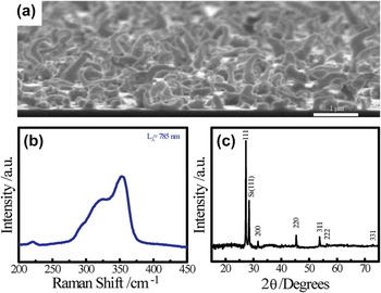
Figure 3(a) presents a cross-sectional scanning electron micrograph of a ZnSnP2 nanowire film grown using 20 nm Sn nanoparticles film over 1 h in the setup described above. The nanowire films appeared dull dark-gray with a uniform density over the substrate area (Supporting info). The optimal temperature for the growth substrate was determined to be between 400 and 440 °C, slightly higher than previously reported for vapor phase synthesis of bulk ZnSnP2 (Refs. Reference Ajmera, Shin and Zamanian19 and Reference Seryogin, Nikishin, Temkin, Mintairov, Merz and Holtz21) but still lower than the temperature reported for ZnSnP2 by melt growth. Reference Davis and Wolfe13,Reference Borshchevskii and Vysotina16,Reference Mughal, Payne and Ray17,Reference Rubenstein and Ure18 For temperatures above 440 °C, no nanowire was observed on the substrate. When the substrate temperature was below 400 °C, nanowires were still deposited, but these materials were not ZnSnP2. Instead, the composition was exclusively Zn3P2.
(a) Cross-sectional scanning electron micrograph of a ZnSnP2 nanowire film grown on 20 nm Sn islands for 1 h. (b) The corresponding Raman spectrum collected with 785 nm excitation source. (c) The powder x-ray diffractogram collected for the same nanowire film.

Figure 3(b) shows the Raman spectrum of as-deposited nanowire films collected with a 785 nm laser. Raman signals spanning 275 to 375 cm−1 were observed. The dominant band in the Raman spectra was at 354 cm−1, assigned to the longitudinal optical (LO) phonon mode of ZnSnP2. Reference Mintairov, Sadchikov, Sauncy, Holtz, Seryogin, Nikishin and Temkin24,Reference Bettini25,Reference Zlatkin, Markov, Stekhanov and Shur26,Reference Lazewski and Parlinski27 The position of this band suggested a crystal structure with some cation disordering, i.e., argued against the chalcopyrite form of ZnSnP2. Reference Mintairov, Sadchikov, Sauncy, Holtz, Seryogin, Nikishin and Temkin24 Two other bands could be discerned at 295 and 329 cm−1, both similarly consistent with phosphorus-based modes normally seen for sphalerite (but not chalcopyrite) ZnSnP2. Reference Mintairov, Sadchikov, Sauncy, Holtz, Seryogin, Nikishin and Temkin24 Within the optimal temperature range for synthesis, no modes at 220, 289, and 347 cm−1 suggestive of Zn3P2 (Refs. Reference Misiewicz28 and Reference Pangilinan, Sooryakumar and Misiewicz29) were observed.
Raman analyses were not sufficient to detect all possible impurity species. Crystalline tin phosphides have no reported strong Raman active modes. Reference Binions, Blackman, Carmalt, O'Neill, Parkin, Molloy and Apostilco30 Nevertheless, the XRD patterns for many crystalline tin phosphides are known. Accordingly, XRD was used to examine both the crystallinity of the as-prepared ZnSnP2 nanowires as well as the purity. Figure 3(c) presents a representative XRD pattern of the as-prepared ZnSnP2 nanowire films. All reflections indexed to ZnSnP2 but in the cubic sphalerite phase, Reference Ryan, Peterson, Williamson, Frey, Maciel and Parkinson14,Reference Francoeur, Seryogin, Nikishin and Temkin31 consistent with the Raman data. A lattice constant of 5.649 ± 0.0019 Å was measured from the x-ray data, in agreement with the reported value for bulk ZnSnP2. Reference Shay and Wernick11 No signatures for trigonal SnP3, cubic SnP, or tetragonal Zn3P2 were observed.
The fundamental reflections of the ordered chalcopyrite and disordered sphalerite ZnSnP2 are the same because such crystal does not exhibit tetragonal distortion, that is, c = 2a. Reference Shay and Wernick11 The level of ordering in ZnSnP2 can be determined from natural atomic superlattice reflections due to formation of (ZnP)2(SnP)2 superlattice in the (201) direction. Reference Francoeur, Seryogin, Nikishin and Temkin31 If the ZnSnP2 were chalcopyrite, a weak (101) reflection at 2θ = 17.5° would be observed in powder XRD. For the nanowire films prepared here, we did not observe a signal consistent with the (101) reflection. Nevertheless, since it may be possible that a small level of chalcopyrite phases exists but doesn't generate a (101) reflection that rises above the detection level. The intensity of the superlattice reflections decreases when the chalcopyrite to sphalerite volume ratio decreases. Reference Ryan, Peterson, Williamson, Frey, Maciel and Parkinson14,Reference Francoeur, Seryogin, Nikishin and Temkin31,Reference Vaipolin, Goryunova, Kleshchinskii, Loshakova and Osmanov32,Reference Francoeur, Seryogin, Nikishin and Temkin33 Hence, we cannot determine that there is absolutely no chalcopyrite phases present in our sample but are confident that our samples are (at least) overwhelmingly predominantly sphalerite.
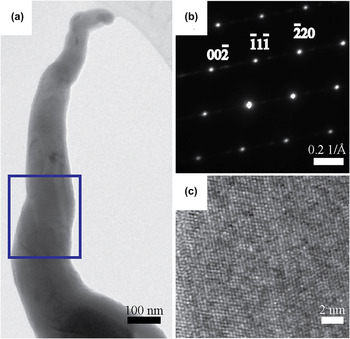
TEM was performed to examine the local composition and crystallinity of as-prepared ZnSnP2 nanowires. Figure 4(a) shows the bright-field TEM image of a representative nanowire grown from 20 nm Sn islands film for 30 min. The as-prepared ZnSnP2 nanowires were tapered, with the base diameter consistently larger than the diameter of the nanowire tip. This morphology was consistent with the premise that the Sn nanoparticle facilitated the crystal growth of ZnSnP2 but was incorporated into the nanowire during growth,
Reference Jeong, McDowell and Cui34
i.e., the Sn particles were both a crystal growing medium and a source for Sn0. This notion was separately validated with growth experiments performed for longer times. Even within the optimal temperature range, the major product switched to Zn3P2 at sufficiently long times, implying the Sn supply, was exhausted. The specific time necessary to deplete Sn and switch the major product to Zn3P2 was a function of Sn nanoparticle size (Supporting Information). The corresponding SAED pattern in Fig. 4(b) was indexed to ZnSnP2 at (110) zone axis and suggested that the nanowire was single-crystalline. The long axis of the nanowires was along the
 $\left\langle {111} \right\rangle$
direction. Figure 4(c) presents the phase-contrast image of the nanowire showing continuous well-defined lattice fringes, corresponding to ZnSnP2 crystal. Since ZnSnP2 does not exhibit tetragonal distortion, the d-spacing values in the SAED patterns on (110) zone axis are the same for chalcopyrite and sphalerite structures. The only difference between the two is the intensity of the diffraction beam, but dynamical effects at the Bragg angle complicate the differentiation between the two phases along the nanowire axis. The absence of the (101) reflection in XRD as well as the broadening of the LO phonon mode in the Raman spectrum substantiated the fact that the as-prepared ZnSnP2 nanowires were sphalerite.
(a) Bright-field diffraction-contrast transmission electron micrograph and (b) the SAED pattern collected from the highlighted area of an isolated ZnSnP2 nanowire. (c) Phase-contrast image showing lattice fringes.

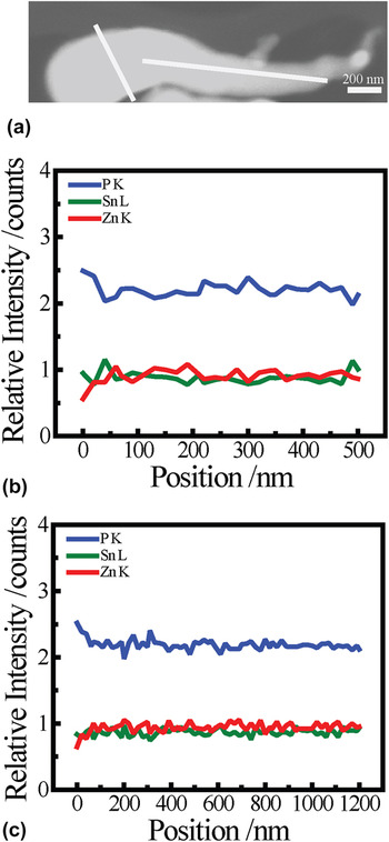
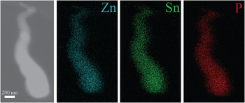
The composition of ZnSnP2 nanowires was assessed using EDS in STEM mode. As presented in Fig. 5, the normalized intensities for Zn Kα, Sn Lα, and P Kα signals were 1:2 cation to anions ratio expected for crystalline ZnSnP2 along both the long and short axes. Separate compositional analyses of the nanowires were performed with Auger Nanoprobe Spectroscopy. An average nanowire composition of 25.7 at.% Zn, 27.5 at.% Sn, and 46.8 at.% P was observed (Supporting Information). The high-angle annular dark field (HAADF) image of the nanowire showed no apparent contrast, implying Zn and Sn was dispersed uniformly throughout the length of the nanowire. Separate elemental mapping (Fig. 6) was also performed to confirm directly the homogeneity of the metals.
Elemental distribution of a representative ZnSnP2 nanowire. (a) HAADF image of the nanowire taken in STEM mode. (b) Radial and (c) axial EDS line scans depicting the relative amounts of Zn, Sn, and P.

The distribution of Zn, Sn, and P in these ZnSnP2 nanowires (different nanowires within the sample) is homogenous throughout the length of the nanowire as shown in EDS mapping.

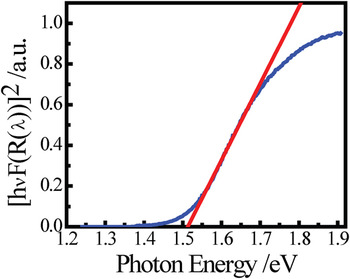
To determine the band gap of as-prepared ZnSnP2 nanowires, wave length-dependent diffuse reflectance was collected and converted to absorption profiles using the Kubelka–Munk function [Eq (1)]. In Fig. 7, the onset of light absorption is plotted using the Tauc relation [Eq (2)] for direct allowed transition. The data in Fig. 7 are consistent with an optoelectronic band gap of approximately 1.51 eV. This value is less than 1.68 eV, the expected band gap for ZnSnP2 with no disorder in the cation distribution, i.e., the chalcopyrite, and is instead in line with the sphalerite form of ZnSnP2. Reference Shay and Wernick11,Reference St-Jean, Seryogin and Francoeur12,Reference Scanlon and Walsh15
 $$F\left( R \right) = {{{{\left( {1 - R} \right)}^2}} \over {2R}} = {\alpha \over s}\quad ,$$
 $${\left[ {hvF\left( R \right)} \right]^2} = A\left( {hv - {E_{\rm{g}}}} \right)\quad .$$
Optical properties of ZnSnP2 nanowire films plotted using Tauc equation. The direct band gap energy was determined to be 1.51 eV.

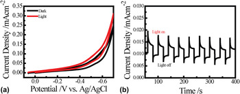
Preliminary photoelectrochemical experiments were performed to gage the conductivity type of the as-prepared nanowire films. Figure 8 presents the photoelectrochemical response for the as-prepared ZnSnP2 nanowire films measured in 20 mM MV and 1 M KCl electrolyte. This electrolyte was chosen for simplicity (since current should pass irrespective to the electrocatalytic activity of the native surface of ZnSnP2 in water) and to facilitate the observation of any photo effect. Specifically, the standard potential of the MV2+/+ couple is sufficiently negative (−0.67 V versus Ag/AgCl at T = 25 °C) that it will induce a strong photocathodic response from a p-type phosphide. Reference Schoenmakers, Waagenaar and Kelly35 Conversely, if the materials are natively n-type, this same couple will induce no discernible photo effect, and the light/dark responses should match each point for point. Figure 8(a) shows the voltammetric response of the nanowire films both in the absence and presence of illumination from an ELH lamp at 100 mW cm−2. The nanowire films exhibited cathodic behavior when illuminated, i.e., a shift in the open-circuit rest potential to more positive values and an increased cathodic current density at very negative applied potentials, i.e., <−0.4 V versus Ag/AgCl. This p-type behavior is consistent with the intrinsic p-type behavior previously ascribed to bulk Zn–IV–P2 crystals. Reference Davis and Wolfe13,Reference Ajmera, Shin and Zamanian19,Reference Goryunova, Kesamanly and Loshakova36 The profile for the photocurrent density–potential relation indicated an extremely low-overall photoelectrode energy conversion efficiency. Still, the chopped photocurrent response of the ZnSnP2 nanowire film in Fig. 8(b) collected at applied bias of −0.4 V versus Ag/AgCl highlights the stability of the cathodic photoresponse.
(a) Current density versus potential response of as-prepared ZnSnP2 nanowire films in the dark (black) as well as under white light illumination (red). (b) Chopped photoresponse of nanowire films when a bias of −0.4 V versus Ag/AgCl was applied. The nanowires showed cathodic behavior when tested in 20 mM MV and 1 M KCl.

IV. DISCUSSION
The data show the preparation of crystalline, phase-pure ZnSnP2 nanowires using Sn nanoparticles as VLS catalysts is possible. The salient features of the presented method are that the growth of ZnSnP2 nanowires did not require any organometallic precursors, PH3(g), or transition metal particles. Rather, solid powder sources of Zn, P, and Sn were used, enabling VLS governed by two chemical reactions. The chemical equation for the in situ generation of P2 and the generation of ZnSnP2 can be written as Eqs. (3) and (4).
 $$2{\rm{Sn}}{{\rm{P}}_3}\left( {\rm{s}} \right)\buildrel \Delta \over \longrightarrow 2{\rm{Sn}}\left( {\rm{l}} \right) + 3{{\rm{P}}_2}\left( {\rm{g}} \right)\quad ,$$
 $${\rm{Zn}}\left( {\rm{g}} \right) + {{\rm{P}}_2}\left( {\rm{g}} \right) + {\rm{Sn}}\left( {\rm{l}} \right) \to {\rm{ZnSn}}{{\rm{P}}_2}\quad .$$
The as-prepared nanowires ZnSnP2 were fully crystalline. The available Raman spectroscopy, x-ray, and electron diffraction studies clearly support this point. However, the crystalline type was not chalcopyrite. Rather, the cumulative data indicated that the materials prepared here possessed randomized intermixing of the Zn and Sn atoms at the cation sites, i.e., the sphalerite phase. The smaller band gap measured here supports this fact. The growth rate of the nanowires was ∼1.5–2 µm h−1. This “fast” crystal growth rate, relative to the growth of bulk crystals over the course of several days, likely promotes disorder in the position of metal cations. Reference Ryan, Peterson, Williamson, Frey, Maciel and Parkinson14,Reference Borshchevskii and Vysotina16 The latter aspect is in line with our previous report where Sn catalysts were also used to grow ZnGeP2 nanowires. Reference Collins, Hankett, Carim and Maldonado7 In that work, although Sn from the growth catalyst was excluded from the as-prepared ZnGeP2 nanowires, the available data similarly suggested that the material had a high degree of cation disorder. Accordingly, we tentatively assign the comparatively low temperatures (relative to those used to grow bulk chalcopyrite ZnSnP2 crystals) and fast crystal growth rate as the most likely factors that favor the formation of the sphalerite phase.
A significant challenge in the deposition of ZnSnP2 nanowires is the unintentional formation of Zn3P2 crystals. Zn3P2 has high tendency to nucleate on a Zn-rich surface in the presence of active P-containing ambients. Reference Bae, Vasekar, VanHart and Dhakal37,Reference Brockway, Van Laer, Kang and Vaddiraju38,Reference Kamimura, Gouveia, Dalmaschio, Leite and Chiquito39 For this system, Zn3P2 was the predominant material deposited if the substrate was not heated at or above 400 °C. Above 400 °C, Zn and P apparently adsorb and dissolve into molten Sn nanoparticles to form ZnSnP2. Since the Sn growth catalysts are consumed at the end of the ZnSnP2 nanowire formation, the tip could become sufficiently Zn-rich to nucleate Zn3P2 from persistent P2(g) as the reactor cooled. Although this possibility could be intentionally exploited to make particular heterojunction contacts, we found that to avoid it, the reactor had to remain under strong vacuum while cooling. When this was done, the nanowires were consistently pure ZnSnP2.
The observed photoelectrochemical behavior suggested a p-type doping, Reference Davis and Wolfe13,Reference Ajmera, Shin and Zamanian19,Reference Goryunova, Kesamanly and Loshakova36 likely arising from Zn vacancies that gave rise to acceptor-type energy levels in ZnSnP2. Reference Scanlon and Walsh15,Reference Miyauchi, Minemura, Nakatani, Nakanishi, Sugiyama and Shirakata40 However, the level of photoactivity in the as-prepared ZnSnP2 nanowires was poor. Specifically, the photovoltage and photocurrent densities observed for the films under these illumination conditions were far less than the values expected for a strongly depleted p-type semiconductor with a band gap of 1.68 eV immersed in such an electrolyte. Reference Heben, Kumar, Zheng and Lewis41 Still, such poor photoresponses for unoptimized materials are neither uncommon nor unexpected. For high aspect ratio semiconductor photoelectrodes, the morphological and electrical properties must be carefully tuned in concert. No attempts were made here to induce a specific level of doping. Rather, the results from these studies is that ‘pure’ undoped ZnSnP2 is likely not attainable by this preparation method. Likely, a vanishingly small number of substoichiometric defects (which can act as electrically active dopants) Reference Goryunova, Kesamanly and Loshakova36,Reference Miyauchi, Minemura, Nakatani, Nakanishi, Sugiyama and Shirakata40 are unavoidable. Still, to make these nanowire films operate with high-external quantum yields for solar energy conversion, rigorous control over the inclusion of additional dopants is necessary, since the dopant level directly controls the Debye length in a nondegenerately doped semiconductor. If these nanowires are not doped enough, then the radii of these nanowires will be too small to support the full potential drop necessary for strong depletion. As we have determined previously, Reference Foley, Price, Feldblyum and Maldonado42 deficiencies in the doping condition of semiconductor nanowires negate any other favorable optoelectronic property and render them useless for solar energy conversion. Still, the studies here do indicate an important aspect relevant to solar water splitting applications. The p-type ZnSnP2 nanowire materials naturally exhibit sufficient chemical and cathodic stability under illumination to permit continued study of their properties for aqueous photoelectrochemistry. Using lattice matching semiconductors, such as GaAs and Ge for the growth substrates, should be helpful in this regard.
V. CONCLUSION
We demonstrated a simple two-zone sublimation approach amenable for the growth and deposition of single-phase crystalline ZnSnP2 nanowires using Zn, SnP3, and molten Sn, with SnP3 as the source of gaseous phosphorous and Sn nanoparticles/nanodroplets as the source of Sn in the crystalline lattice. The utility of two separate heating zones in the reactor is to separately heat the substrate and source materials to temperatures that promote the formation of ZnSnP2 over Zn3P2 or any other impurity material. The cumulative Raman, x-ray, and microscopic structural characterizations showed crystalline ZnSnP2 nanowires with the sphalerite lattice type. This preparation route yielded photoactive ZnSnP2 nanowire films with native p-type character. These studies add to the available types of phosphides that can be explored as nanostructured light harvesting elements in photoelectrochemical or photovoltaic applications.
Supplementary Material
To view supplementary material for this article, please visit http://dx.doi.org/jmr.2015.195.
ACKNOWLEDGMENTS
S.L. acknowledges Dr. Junsi Gu and Ms. Meagan Cauble with helpful discussions. This work is supported by the National Science Foundation under Grant No. DMR-1054303.