Introduction
The manufacturing of complex three-dimensional (3D) structures at various scales is one of the main themes of the fourth industrial revolution. The 3D manipulation of materials in 3D printing is key to such manufacturing processes. Various strategies have been tried to fabricate 3D structures in a diversity of materials from 3D printed food to monolithic homes for space explorers. Printing of extremely small structures is a challenging task because of hardware and material limitation. Technologies capable of fabricating 3D microstructures with nano- or micro-meter resolutions are valuable tools for the development of nanotechnology, photonics, and biotechnology. Techniques such as ink-jet printing,[Reference Gratson, García-Santamaría, Lousse, Xu, Fan, Lewis and Braun1] self-assembly,[Reference Park, Harrison, Chaikin, Register and Adamson2] layer-by-layer assembly,[Reference Fleming, Lin, El-Kady, Biswas and Ho3] lithography-electroplating-modeling,[Reference Tolfree4] interference lithography,[Reference Divliansky, Mayer, Holliday and Crespi5] focused ion beam milling,[Reference Reyntjens and Puers6] and laser-based photolithographic techniques[Reference Bertsch, Lorenz and Renaud7, Reference Lee, Kang, Park, Rhie, Hahn and Cho8] are being used to fabricate 3D structures for various applications. Two-photon stereolithography (TPS) has the potential to overcome many current limitations and is becoming the tool of choice for microstructuring a diverse range of material into complex functional structures. Scalable high-resolution manufacturing techniques can add value to the existing technologies or give rise to yet more innovative ones.
The TPS process is based on the non-linear absorption of light by materials. Two-photon-induced chemistry is possible only with the help of high-intensity lasers. In the TPS process, two-photon initiated processes take place at the focus of a laser beam where the intensity is the highest. Such a stringent intensity requirement leads to high-spatial confinement of two-photon processes. This spatial confinement is key to the TPS technique because it allows confined photoinduced chemical reactions. Such chemical reactions can be spatially manipulated inside a photoactive material by changing the laser focus inside the material, leading to direct writing of photoinduced chemical changes. Because of these attributes, TPS is also called two-photon direct writing or laser direct writing.[Reference Prabhakaran9] Polymerization, photochemical reactions, photodegradation, photoreduction reactions etc. can be initiated by the two-photon process.[Reference Lee, Kim, Yang and Park10–Reference Zhang, Chen, Xia and Sun12] Two-photon-induced polymerization reactions have been the mainstay of TPS research by far.[Reference Yang, Lim, Son, Kong, Lee, Kim and Park13–Reference LaFratta, Baldacchini, Farrer, Fourkas, Teich, Saleh and Naughton17]
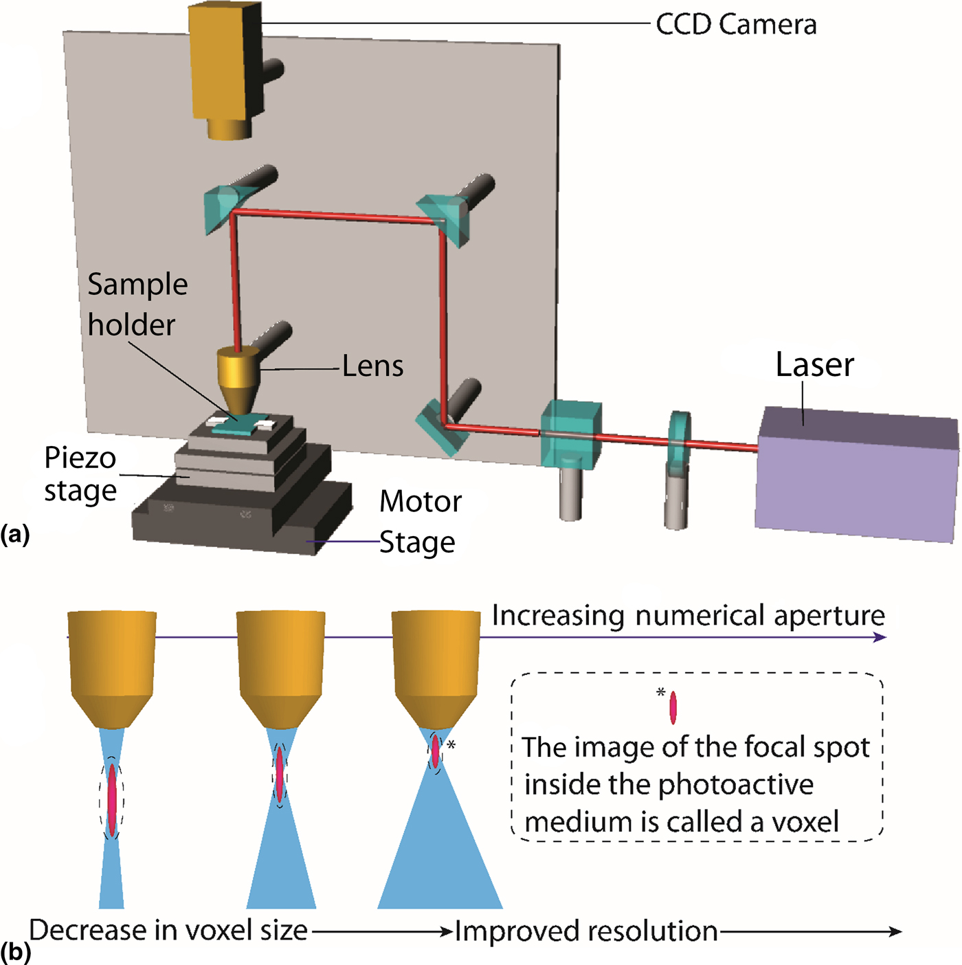
A UV-based polymerization technique for fabrication 3D polymer structures was discovered by Kodama in 1981.[Reference Kodama18] This led to the development of UV stereolithography and eventually TPS.[Reference Ikuta and Hirowatari19–Reference Maruo and Ikuta21] An example of a TPS system can be seen in Fig. 1(a). It consists of a laser source (e.g., Ti:sapphire laser) capable of producing ultrashort pulses (one pulse lasts a few tens to hundreds of femtoseconds) of infrared radiation at high-repetition rates (number of pulses per second). The combination of ultrashort pulses (e.g., 100 fs) and high-repetition rate (e.g., 80 MHz) allows the concentration of immense energies into the laser focus while limiting photo-induced damage to materials undergoing photochemical changes during the lithographic process. The laser is focused onto a photoactive material placed on a thin glass or plastic substrate by means of a lens with a high numerical aperture (NA). The NA defines the angles at which light can enter and exit a lens and defines the shape of the focused laser beam inside the photoactive medium. The shape of the focused laser beam in turn defines the smallest feature that can be fabricated by a given lithographic setup. This is because photo-induced chemical reactions during TPS are confined to the focus of the laser. The smallest feature formed during fabrication is a chemical image of laser focus. This image of the focused laser beam chemically reproduced (through photoreactions) inside the optically active material is called a voxel or a volumetric pixel. The voxel often has a prolate spheroidal shape and can be regarded as the fundamental building block of a microstructure fabricated by TPS. Key aspects of NA and its effect on voxels are summarized in Fig. 1(b). A higher NA leads to a tighter focus and hence smaller voxels, increasing the resolution of the fabricated structure.[Reference Lee, Kim, Yang and Park10]
(a) Schematic diagram of a TPS system. (b) The effect of NA on voxel size and resolution.

Computer-aided design is used to produce 3D structures for TPS. The computer-aided design data are made suitable to be fed to the TPS system by dedicated software. This process of transcribing 3D design data to suit the TPS system is called slicing. During slicing, the 3D structure is converted into a collection of planes, which when merged, could recreate the 3D structure. The planar data from slicing define the movement of the laser focus along a plane. There are different scanning regimes for the laser beam to create a 3D structure depending on the constraints of application and time. Two such laser scanning schemes are called the raster scanning method and contour scanning method. With raster scanning, the whole volume of the structure is scanned to create a totally solidified structure. In contour scanning, the profile (outer and inner walls) of the structure is scanned.[Reference Lee, Kim, Yang and Park10] The contour scanning method leads to faster fabrication of microstructures, although in some cases it may lead to inadequate mechanical properties in the final cured structures. Complex slicing techniques have been developed to overcome mechanical defects in fabricated structures.[Reference Park, Lee, Yang, Kong and Lee22]
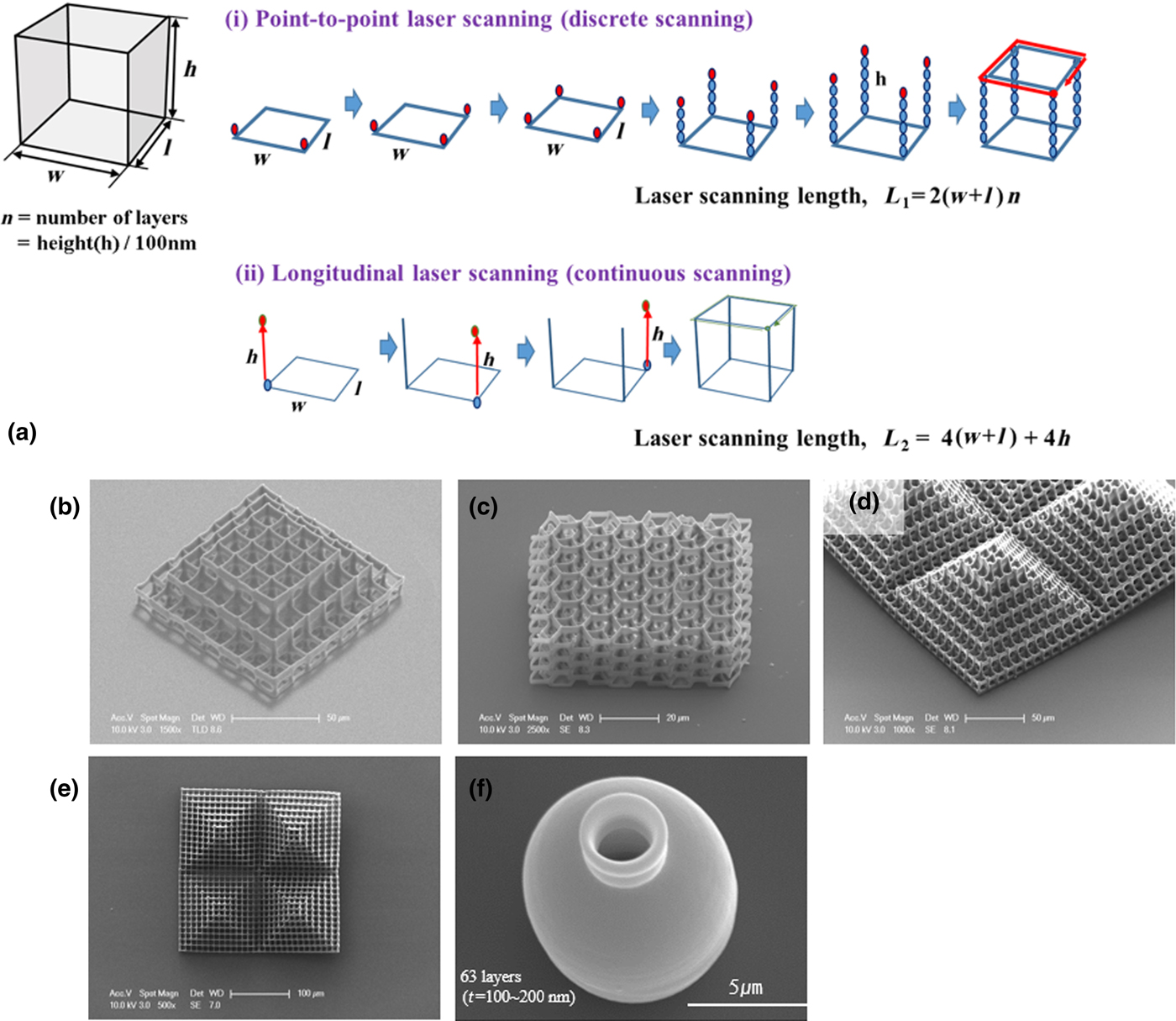
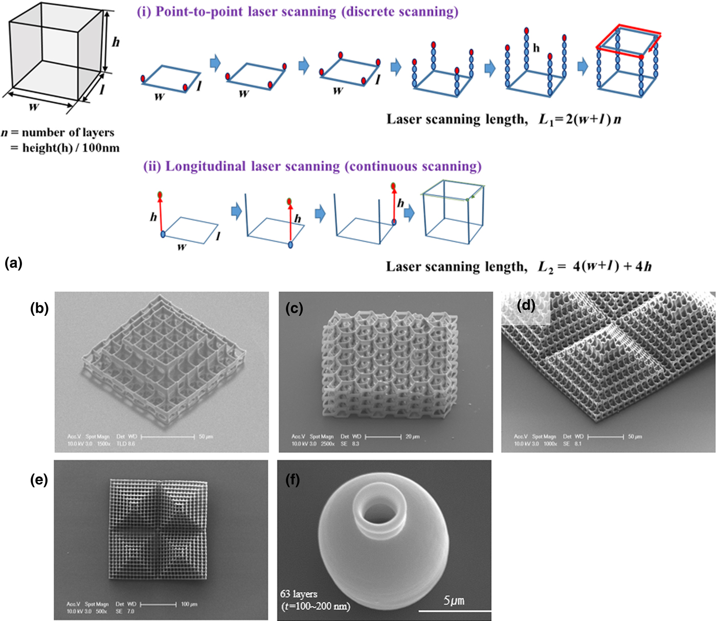
All microstructures fabricated by TPS can be considered an orderly arrangement of interconnected voxels in space. The laser focus is scanned along the X, Y, and Z axes inside the photoactive materials by mechanical or optical manipulation. The TPS system shown in Fig. 1(a) includes piezo-stages capable of moving a sample along all three spatial dimensions a few hundred micrometers during fabrication. Motor stages allow manipulation of the sample hundreds of micrometers along X and Y axes before or after fabrication to enable fabrication of arrays of microstructures. The piezo-stages are exclusively used for manipulation of the laser focus inside the sample by movement along the three spatial axes. The maximum length and breadth of the microstructures that can be created using the TPS systems in Fig. 1(a) depend on the XY piezo-stages. The height of microstructures depends on the movement of the piezo-stage along the Z axis and the NA of the lens. Most common fabrication systems use transparent thin glass or flexible plastic substrates (150–200 µm thick) with photoactive samples (called photoresists) on them for fabrication. The laser is focused through the substrate into the sample during fabrication. It is important to fix the fabricated structure to the substrate during fabrication because an unfixed structure will be washed away during the post-fabrication development process. To stably fix the microstructure on the substrate, it is important to find the right z-position of laser focus (height of laser focus) at the interface of the photoactive sample and the substrate. Such a position leads to voxels polymerized directly on the surface of the substrate and to good adhesion between the structure and the substrate. In commercial TPS systems there are functioning autofocus systems that estimate the interface between the substrate and the sample through optical techniques. Periodic structures such as woodpiles or micro-pillar arrays are useful for optically active microstructures such as photonic crystals, wave guides, and metamaterials.[Reference Vyatskikh, Delalande, Kudo, Zhang, Portela and Greer23–Reference Meza, Zelhofer, Clarke, Mateos, Kochmann and Greer26] TPS has been applied to the fabrication of micro-lenses with gentle curvature used for optical imaging.[Reference Malinauskas, Gilbergs, Žukauskas, Purlys, Paipulas and Gadonas27, Reference Guo, Xiao, Zhai, Li, Xia and Huang28] Hexahedral structures such as the cuboidal structure seen in Fig. 2(a) are very important for many different applications. They feature in optically active structures[Reference Serbin, Egbert, Ostendorf, Chichkov, Houbertz, Domann, Schulz, Cronauer, Frhlich and Popall29] and cell growth scaffolds for biotechnological applications.[Reference Weiß, Schade, Laube, Berg, Hildebrand, Wyrwa, Schnabelrauch and Liefeith30, Reference Baldacchini, Nuñez, LaFratta, Grech, Vullev and Zadoyan31] The fabrication of such structures often takes a long time using the traditional point-to-point (layer by layer) scanning method shown in Fig. 2(a)-(i). In this method, the vertical edges of the cuboidal structure are fabricated in a loop-like movement while the laser focus is alternated between the four corners of the structure. After each loop the focus moves up along the Z-direction to incrementally write the vertical edge. This leads to slow progression of fabrication, hampering the study of applications. We recently developed an accelerated scheme for the fabrication of hexahedral structures called the longitudinal scanning method. This method is based on the simultaneous movement of the x, y and z piezo-stages of the TPS system, resulting in the writing scheme seen in Fig. 2(a)-(ii). In the case of a hexahedral structure that is 10 µm × 10 µm × 10 µm in length, the fabrication time of the continuous laser scanning method was 70 times faster than the fabrication time of point-to-point laser scanning.[Reference Ha, Prabhakaran, Son, Lee and Yang32] Some structures fabricated using the longitudinal scanning scheme can be seen in Figs. 2(b)–2(e). However, structures containing curved surfaces, as seen in Fig. 2(f), are more conveniently fabricated by the point by point scanning method in layer [Fig. 2(a)-(i)].[Reference Park, Lee, Yang, Kong and Lee22] Both methods [Fig. 2(a)] can be combined to effectively manufacture complex functional microstructures.
(a) Two different concepts of direct writing mesh structures. (a-i) A schematic diagram showing the point-by-point laser scanning method. The red dots represent the progression of the laser focus during fabrication. (a-ii) The longitudinal scanning method where the vertical edges are fabricated by scanning along the z-axis in a continuous movement. (b–e) Various structures fabricated using the longitudinal scanning method. (f) A microstructure with curved surfaces produced by the layer by layer scanning method. Reproduced with permission from Ref. Reference Park, Lee, Yang, Kong and Lee22 (AIP Publishing) and Reference Ha, Prabhakaran, Son, Lee and Yang32 (Springer Nature).
New precursors for functional microstructures
Ceramic-based TPS
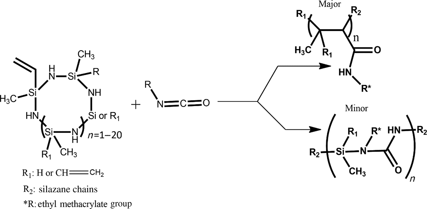
Ceramics are hard wear-resistant, chemically inert, nonmagnetic, electrical, and thermal insulators. Ceramic microstructures are interesting in tribological applications, as well as chemically inert microfluidics. Different approaches to fabricate 3D ceramic microstructures using TPS have involved using preceramic polymers or ceramic-powder mixed polymers.[Reference Yang, Deschatelets, Brittain and Whitesides33–Reference Provin, Monneret, Le Gall and Corbel35] We synthesized a new ceramic precursor photoresist (SiCN) by reacting polyvinylsilazane and 2-isocyanoethyl methacrylate, as shown in Fig. 3. Photocured films of SiCN were seen to have improved mechanical properties on thermal curing them at about 600 °C. The organic materials in the photocured films of SiCN were burned away above 600 °C, eventually leading to the formation of a ceramic film containing inorganic components. The Young's modulus of the photo-thermally cured films reached as high as 60 GPa for curing at 800 °C. Features as small as 210 nm could be fabricated during microfabrication using the SiCN ceramic precursor.[Reference Lim, Son, Yang, Pham, Kim, Yang, Lee and Park36, Reference Pham, Kim, Lim, Park, Yang and Lee37]
Synthesis of ceramic precursor photoresist.

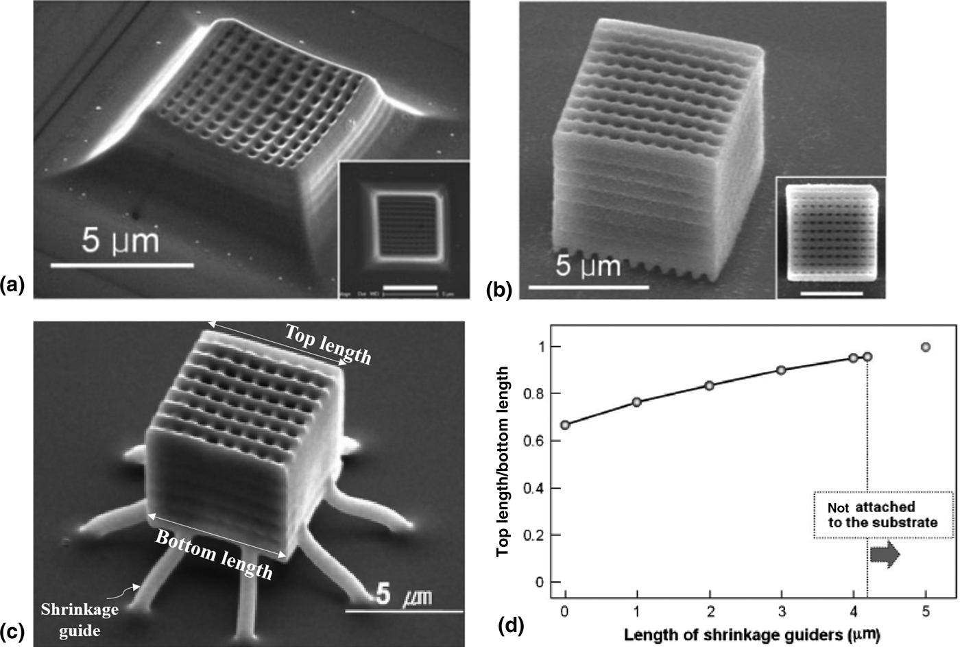
After fabrication, the microstructures were pyrolyzed at 600 °C to form a ceramic microstructure. The pyrolyzed structures underwent shrinking; the strong interaction between the bottom layer of the structure and the surface of the substrate reduced shrinkage in the bottom layers of the pyrolyzed structure. However, the lateral edge length of the top surface was drastically reduced leading to a pyramidal structure seen in Fig. 4(a). This shrinkage results from the removal of the organic materials in the precursor during pyrolysis. To reduce the shrinkage problem, silica nanoparticles approximately 10 nm in diameter were added to the ceramic precursor photoresist. A 40 wt% loading of silica particles in the photoresist lead to ceramic structures with weak interfacial adhesion to the substrate. The structures also showed a relatively isotropic shrinkage due to sliding free from the substrate during pyrolysis [Fig. 4(b)]. This demonstrated that pyrolytic shrinkage can be improved by controlling the photoresist composition.
(a) Non-uniform shrinkage at the top and base of a fabricated structure because of the effect of the substrate. (b) Isotropic shrinkage of a ceramic structure by adding silica nanoparticles. (c) Minimizing shrinkage in a ceramic structure by guiding structures. The ceramic structure is fabricated on guide pillars that elongate and minimize the effect of shrinkage on the microstructure. (d) A study of the dependence of shrinkage on the length of the shrinkage guiders. Reproduced with permission from Ref. Reference Lim, Son, Yang, Pham, Kim, Yang, Lee and Park36 (John Wiley and Sons) & Reference Pham, Kim, Lim, Park, Yang and Lee37 (John Wiley and Sons).

Another strategy to avoid shrinkage during pyrolysis ceramic precursor structures is to pre-compensate the non-uniform shrinkage seen in Fig. 4(c). In this method, the microstructure is fabricated on slanted bars that act as shrinkage guides. The length of the shrinkage guides required to fabricate a good ceramic microstructure depends on the extent of shrinkage during heating. The ratio of top side length to bottom side length of a symmetric hexahedral structure as in Fig. 4(c) defines the symmetry of the structure and the variation of its shrinkage. When the ratio is close to 1, the structure has undergone uniform shrinkage. As the shrinkage guide is longer, the structure has less influence from the substrate and the shrinkage of the ceramic microstructure is uniform, leading to a symmetrically shrunk structure. As shown in Fig. 4(d), the ratio was seen to approach 1 when the length of the guider was close to 4 μm. A further increase in guider length did not significantly change the ratio between the top and the bottom edge.
Quantum dot-based TPS
Quantum dots (QDs) are inorganic semiconductor nanocrystals that can be applied to solar cells, photodetectors, and bioimaging devices.[Reference Steckel, Snee, Sullivan, Zimmer, Halpert, Anikeeva, Kim, Bulovic and Bawendi38–Reference Park, Prabhakaran, Jang, Lee, Lee, Lee, Hur, Kim, Cho, Son, Yang and Lee41] Functionalization of QDs plays an important role in making them compatible with interactions with functional materials. Incorporating inorganic nanomaterials into polymer precursors is a common strategy to improve the refractive index of eventual photocured structures.[Reference Smith, Pendry and Wiltshire42] Surface functionalization of nanomaterials helps reduce their surface energy and tendency toward aggregation. The reactive groups in molecules and polymers used for surface functionalization help with further manipulation of nanoparticles or their composites with polymers. The functionalization of QDs with photoreactive ligands allows the densification of QD films by light. Such densification leads to ordering of nanoparticles as well as changes in their optical properties.
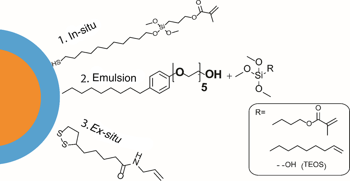
Three different approaches to making a patternable QD can be seen in Fig. 5. The first one involves an in-situ approach where a ligand containing thiol at one end and hydroxy group at the other end is used to passivate the freshly synthesized QDs. Since thiols show strong interaction with the QD surface, the ligand forms an outer sphere containing –OH groups around the nanoparticle. This is followed by a reaction with a second ligand containing alkoxy silane groups at one end and methacrylate group at the other. The in-situ process makes QDs with a polymerizable methacrylate corona. This technique was used to functionalize red, green, and blue cadmium containing (II–VI) QDs.[Reference Park, Prabhakaran, Jang, Lee, Lee, Lee, Hur, Kim, Cho, Son, Yang and Lee41, Reference Jang, Prabhakaran, Chandran, Park and Lee43] The in-situ photopatternable functionalization allows patterning of QDs onto glass and flexible substrates. The UV-induced densification of films of photopatternable QDs showed increased photoluminescence compared with QDs without functionalization.[Reference Park, Prabhakaran, Jang, Lee, Lee, Lee, Hur, Kim, Cho, Son, Yang and Lee41] Such functionalization improves the uniform mixing of QDs into photoresists, facilitating easy fabrication of QD-doped 3D structures.
Different strategies for the functionalization of QDs to make them photopatternable.
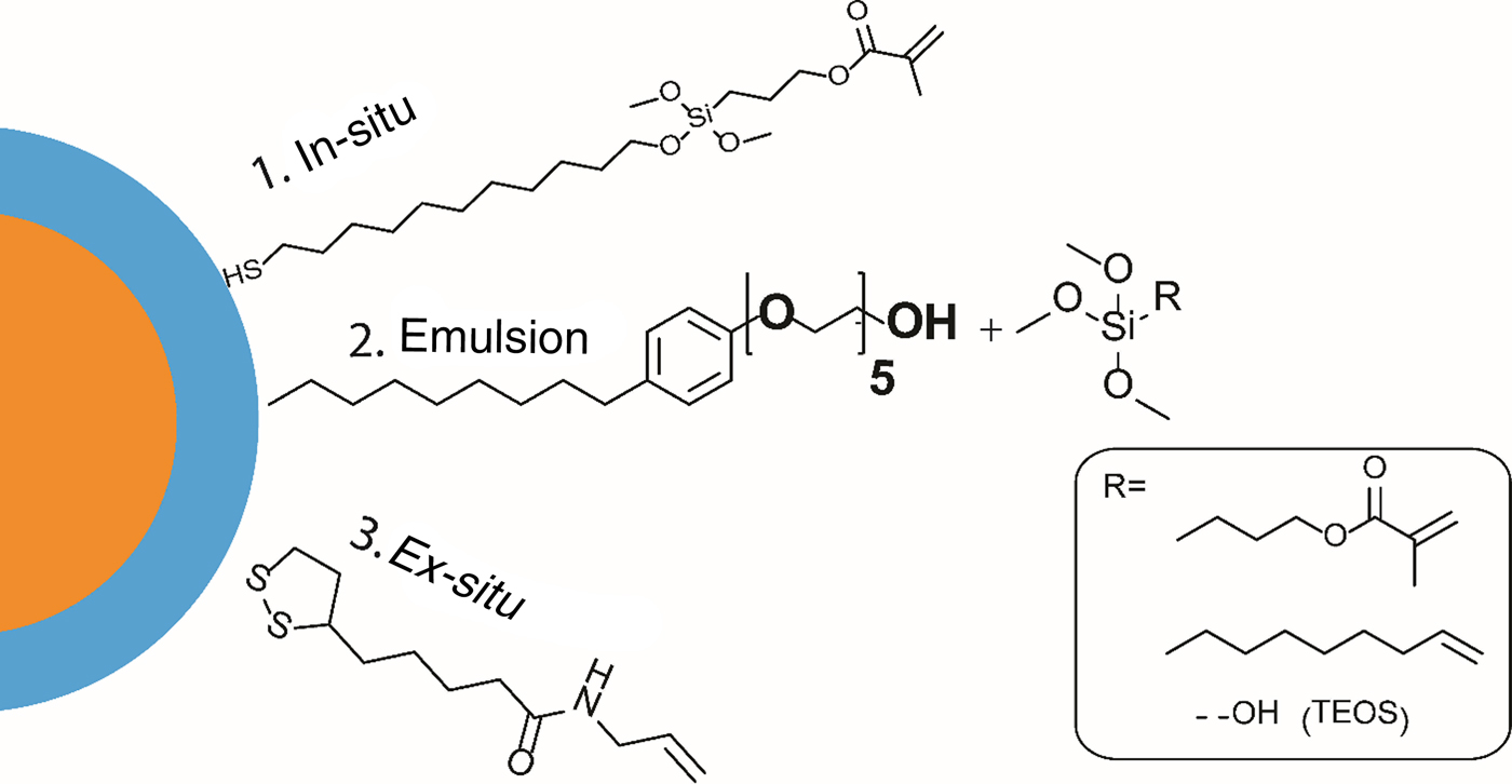
The second approach to create patternable QDs can be used in principle to incorporate a type of nanoparticle because it does not depend on the surface interaction between the nanoparticle and the ligand. The second approach shown in Fig. 5 is based on a micro-emulsion technique. A surfactant is used to create micro-emulsions encapsulating nanoparticles yielding emulsions containing –OH groups on its outside. These emulsions are compatible with sol–gel reactions. Depending on the selection of sol–gel precursor a large variety of surface groups can be functionalized on the QDs as seen in Fig. 5. The QDs functionalized by this approach are encapsulated by silica shells and functionalized with cross-linkable groups on the outer surface. Similar to the QDs functionalized by the in-situ method, the QDs prepared with the micro-emulsion technique are highly compatible with organic photoresists, and could also be dispersed well in hybrid organic–inorganic photoresists.[Reference Krini, Ha, Prabhakaran, Mard, Yang, Zentel and Lee44]
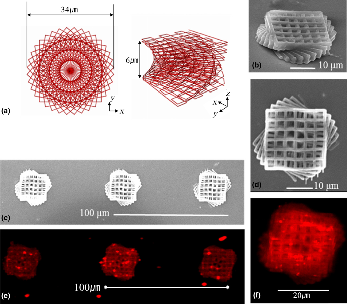
Cadmium-based QDs have been studied for the fabrication of QD-incorporated microstructures. However, cadmium-based QDs have limited applications due to their toxicity. Figure 6 shows a cadmium-free photopatternable QD that has a ligand containing dithiolane group at one end and an ene-functionalization at the other end.[Reference Park, Teng, Jung, Prabhakaran, Ha and Lee45] A twisted polymer structure was fabricated with the SCR-500 photoresist doped with cadmium-free QDs. The structure demonstrated the viability of uniformly embedded QDs in a 3D microstructure.
SEM and confocal micrographs of the 3D twisted structure. (a) The design of a 3D twisted structure. (b–d) SEM images of red QDs incorporated into a 3D twisted structure. (e) and (f) Top views of the 3D twisted structure by confocal microscopy. Reproduced with permission from Ref. Reference Park, Teng, Jung, Prabhakaran, Ha and Lee45 (OSA Publishing).

The addition of nanoparticles increases the threshold power of polymerization in photopolymers while also causing heating effects due to particle–laser interactions. Higher loading of nanoparticles or metal/semiconductor precursors can lead to heating effects and the collapse of microstructures. Such effects can be controlled by regulating both the quantity of nanoparticles added as well as the laser power during TPS. We used 0.6 wt% of QD in the photoresist to avoid such effects.
Metal patterning
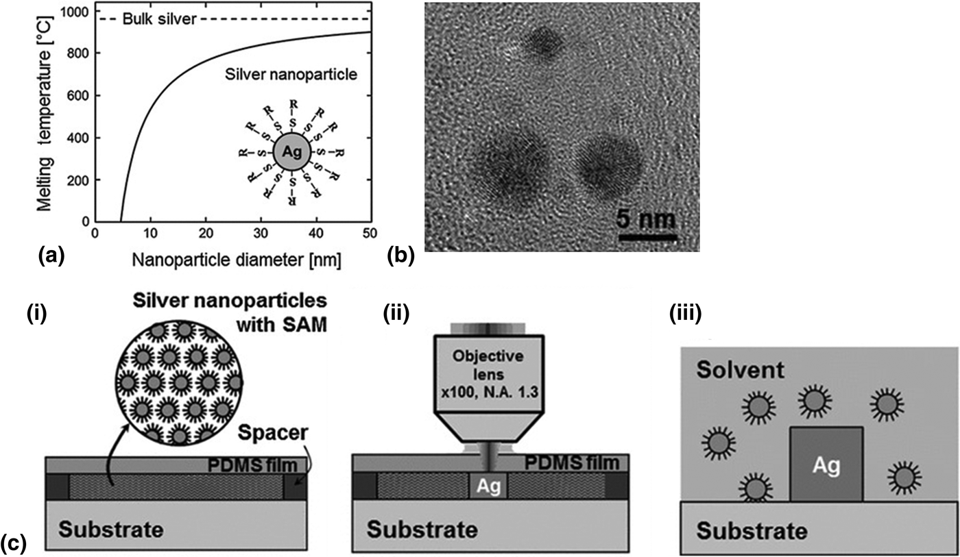
The fabrication of electrically conductive micropatterns has been studied for various applications such as flexible electrical circuits, organic thin film transistors, and solar cells.[Reference Ko, Pan, Grigoropoulos, Luscombe, Fréchet and Poulikakos46–Reference Chung, Bieri, Ko, Grigoropoulos and Poulikakos48] The metallic wires and structures are integrated conventionally by vacuum deposition or photolithography processes. Such processes often require expensive vacuum conditions, high-processing temperature, and toxic chemicals with many fabrication steps. The high-intensity pulsed lasers provide an easier alternative to achieving patterning of metals such as silver and gold. There have been several studies for metal patterning by femtosecond laser direct writing. For example, assembly of metal nanoparticles induced by the femtosecond laser is an effective method to form desired metal patterns.[Reference Wang, Liu, Zhang, Wang, Wang, Xia, Chen, Ding and Sun49–Reference Wang, Zhang, Xia, Chen, Lee and Sun50] In addition, the femtosecond laser used in the TPS process can also be used to induce physical changes and inorganic chemical reactions.[Reference Stellacci, Bauer, Meyer-Friedrichsen, Wenseleers, Alain, Kuebler, Pond, Zhang, Marder and Perry51–Reference Prabhakaran, Jang, Son, Yang and Lee57] Solvated metal precursors can be directly photoreduced to make metallic structures.[Reference Ishikawa, Tanaka and Kawata55] Silver and gold nanoparticles have been studied for their two-photon optical activity.[Reference Wenseleers, Stellacci, Meyer-Friedrichsen, Mangel, Bauer, Pond, Marder and Perry58, Reference Yuan, Khoury, Hwang, Wilson, Grant and Vo-Dinh59] The optical interactions of noble-metal nanoparticles with lasers are also associated with the generation of heat. Silver nanoparticles with diameters <10 nm have a very low melting point and can be melted by the heat generated by laser interactions. The size dependence of the melting point of silver nanoparticles can be seen in Fig. 7(a).
(a) Variation in melting point of silver nanoparticles with nanoparticle size. (b) TEM image of silver nanoparticles. (c-i) Setup for fabricating sintered silver structures. (c-ii) Fabrication of sintered silver lines from nanoparticle films. (c-iii) Development of fabricated structure by washing away the unsintered nanoparticles. Reproduced with permission from Ref. Reference Son, Yeo, Moon, Lim, Hong, Nam, Yoo, Grigoropoulos, Yang and Ko60 (John Wiley and Sons).

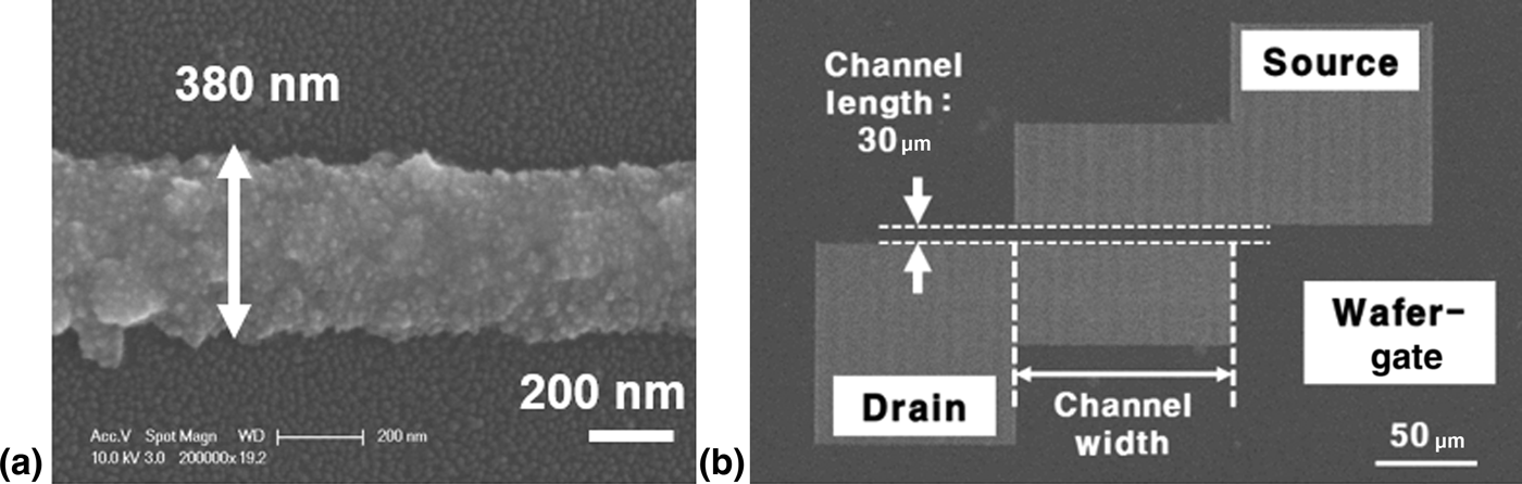
The pulse width of the femtosecond laser used in the TPS process is very short compared with the onset of thermal diffusion time in nanoparticle dispersions. Controlled heating achieved by the laser led to significant advances in the resolution of fabricated silver structures. Metal nanoparticles are sintered by the heat generated by light–nanoparticle interaction to fabricate sub-micrometer-sized metal patterns.[Reference Son, Yeo, Moon, Lim, Hong, Nam, Yoo, Grigoropoulos, Yang and Ko60, Reference Son, Yeo, Ha, Lee, Hong, Nam, Yang and Ko61] Homogeneous dispersion of the silver nanoparticles was achieved by encapsulating them using a functional self-assembled monolayer. A transmission electron microscopy (TEM) image of silver nanoparticles can be seen in Fig. 7(b). The nanoparticle dispersions were spin-coated onto a desirable substrate such as glass or silicon wafer. A polydimethylsiloxane (PDMS) film was placed above the spin-coated film, and the PDMS film and the substrate on which the silver nanoparticles were spin-coated were separated by a spacer, as seen in Fig. 7(c)-(i). During microfabrication, the nanoparticle films were selectively sintered by focusing the working laser through the transparent PDMS film into the substrate, as seen in Fig. 7(c)-(ii). After fabrication, the unreacted silver nanoparticles are washed away to reveal the fabricated structures, as shown in Fig. 7(c)-(iii). Uniform sintered metal lines with a minimum width of 380 nm can be fabricated by the TPS process, as shown in Fig. 8(a). Using laser scanning paths from computer-aided design data, arbitrary two-dimensional (2D) metal patterns could be simply fabricated. As shown in Fig. 8(b), the minimum measured resistivity (2.0 × 10⁻⁷ Ω m) is about 12.5 times higher than that of bulk silver (1.59 × 10⁻⁸ Ω m). Metal conductor patterns with 30 µm in channel length were directly fabricated using the selective femtosecond laser sintering process. This result demonstrates that fabricated silver patterns can be used for an electrically conductive part of microdevices. This approach offers remarkable advantages as a one-step, direct, high-resolution process for the fabrication of nanoscale electronic components.
SEM images of (a) the fabricated metal line and (b) the fabricated organic field-effect transistor. Adapted/reproduced with permission from Ref. Reference Son, Yeo, Moon, Lim, Hong, Nam, Yoo, Grigoropoulos, Yang and Ko60 (John Wiley and Sons) and Reference Son, Yeo, Ha, Lee, Hong, Nam, Yang and Ko61 (Elsevier).

Functional microstructures
Micromixers for fluidic application
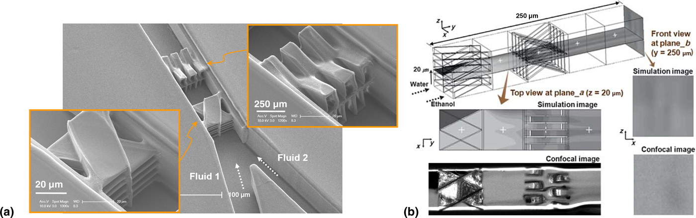
Microfluidic technologies have been widely used in chemical as well as biologic applications. Mixing different components is a fundamental requirement in many studies involving microfluidics. The design and fabrication of novel micromixers is an active field of research in microfluidics.[Reference Jeon, Malyarchuk, White and Rogers62, Reference Park, Lee, Moon and Yang63] Conventional microelectromechanical system (MEMS) processes and soft lithographic approaches require many sequential structures for fabricating arbitrary mixing structures. Many efficient micromixers feature long channel length (the distance in the microfluidic channel over which efficient mixing is achieved) due to limitations in achieving complex mixer designs.[Reference Stroock, Dertinger, Ajdari, Mezić, Stone and Whitesides64–Reference Kim, Lee, Kwon and Ahn66] A detailed review of various approaches to fabricate micromixers with TPS techniques has been highlighted in a recent review.[Reference Xu, Zhang, Xia, Dong, Ding and Sun67] Our approach involved a crossing manifold micromixer (CMM) with a sequential configuration of horizontally and vertically CMMs (H-CMM, V-CMM) which has been proposed to achieve good mixing within a short distance in a microfluidic device.[Reference Lim, Son, Jeong, Yang, Kong, Lee and Kim68] The CMM micromixer (H-CMM and V-CMM) was fabricated inside a microfluidic channel with a height of 50 µm using TPS. The horizontally and vertically CMM (H-CMM, V-CMM) can be seen in Fig. 9(a). After the fabrication of the micromixers in the channel, the microfluid injection system was sealed by bonding with PDMS slabs with two inlet and one outlet holds.
(a) SEM image of the 3D micromixer fabricated in the micro-channel. The insets show horizontally and vertically crossing manifold mixers, while (b) shows a fluorescence image of the mixing process. Reproduced with permission from Ref. Reference Lim, Son, Jeong, Yang, Kong, Lee and Kim68 (Royal Society of Chemistry).

The efficiency of the micromixer was studied by evaluating the mixing of a stream of water with a rhodamine B solution in ethanol. Rhodamine B is a highly fluorescent molecule. The extent of mixing can be evaluated by the fluorescence of the mixed solution. Fluorescence images of the mixing process in the microfluidic channel equipped with H-CMM and V-CMM can be seen in Fig. 9(b). The H-CMM can be seen to the right and the V-CMM to the left. The dark liquid inside the channel is water and the white (fluorescent) liquid is ethanol containing rhodamine B (0.1 wt%). The mixing occurs from right to left, and all of the mixture can be seen fluorescing after it passes the H-CMM. The mixing is further enhanced by the V-CMM. Based on theoretical simulations, the distance between H-CMM and V-CMM was set at 50 µm. Both H-CMM and V-CMM consisted of six channels which split the liquid flow into 36 segments, resulting in a mixing efficiency of 90% over a short channel length of 200 µm in the microfluidic channel. These micromixers were fabricated with a short channel length of 200 µm inside the microchannels and showed very efficient mixing efficiency of 90%. Thus, TPS can be an effective manufacturing technique for fabricating functional components inside microfluidic channels for lab-on-a-chip applications.
Micro-manipulators
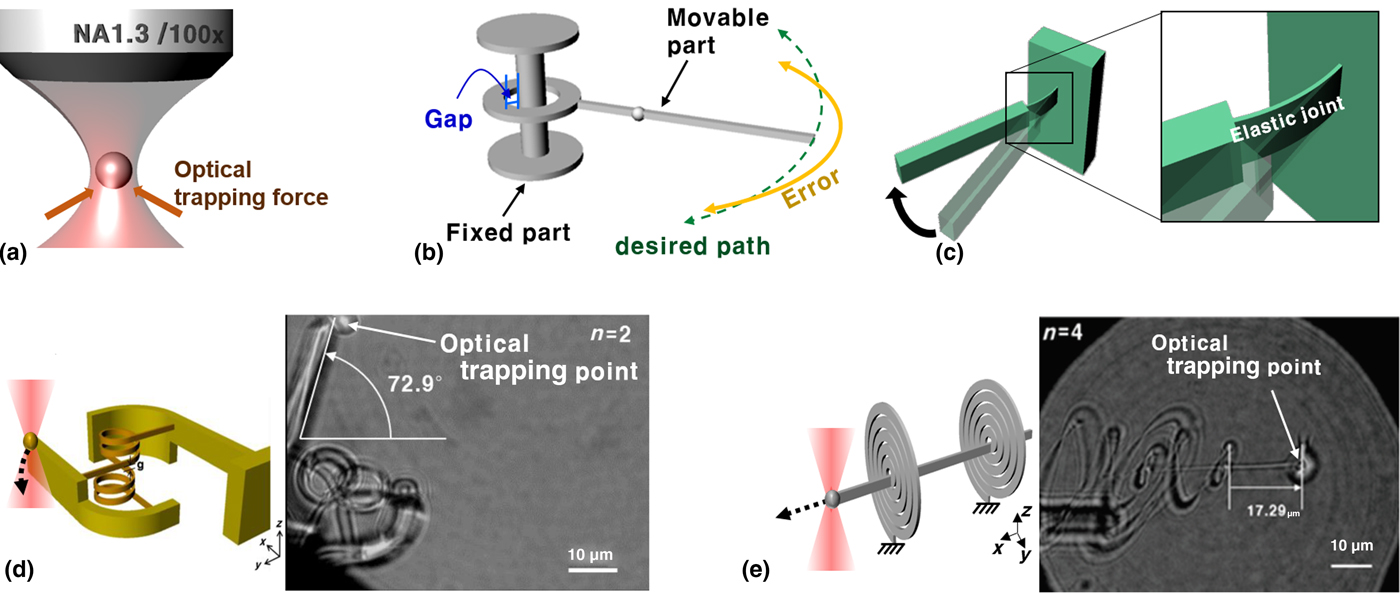
Micro-manipulators are functional structures that find applications in the manipulation of objects. Micromanipulation may involve the manipulation of cells or inanimate objects with an aim to sort, assemble, or use them for a specific application. Micro-manipulators can be driven by many different forces such as chemical reactions, microorganisms, magnetic force, etc. Optical trapping force is a key method to actuate a micro-manipulator. It is also called optical tweezing force. When a laser beam is focused onto an object, the optical trapping force is generated on the object toward the focal point of the laser beam, as graphically represented in Fig. 10(a). It has the potential to precisely manipulate objects and materials.
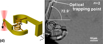
(a) Concept of optical trapping force generated by a laser beam. Illustrations of micro-joints based on (b) kinematic design and (c) elastic design concept. Optical driven (d) rotational and (e) linear joints based on elastic design. Reproduced with permission from Ref. Reference Ha and Yang74 (OSA Publishing) and Reference Ha and Yang75 (IGI Global).

Optical trapping force has been used to drive micro-joints for rotational and translational movement. Most micro-joints are generally based on a kinematic design concept. Such joints have a gap between moving part and fixed part, as seen in Fig. 10(b).[Reference Wautelet69] Due to this gap, the joint has a motion error from the desired path and a large friction force that inhibits micro-manipulation.[Reference Cugat, Delamare and Reyne70, Reference Trimmer71] Therefore, joints based on kinematic design have inherent difficulties in preventing various precise motions at a micro-scale. An alternative is the micro-joint based on the elastic design concept seen in Fig. 10(c). Because there is no gap in the whole structure with the elastic design, friction force is not generated on elastic joints. Therefore, the moving elements can be precise.
In the case of elastic micro-rotational joints, they have been designed based on a cross-spring, which is the conventional design for precise rotational movement.[Reference Hongzhe and Shusheng72, Reference Zhao and Bi73] However, the cross-spring has a small range of rotational angle because the elastic joint has limited deformation. As shown in Fig. 10(d), a modified rotational joint including a helical structure can achieve much greater rotational movement, as the number of turns of the helical structure extended the length of the structure that could be elastically deformed.[Reference Ha and Yang74] It causes the range of rotational angle to increase. In the case of an elastic micro-translational joint based on the elastic design, it was designed with additional spiral structures for large and precise translational movement, as seen in Fig. 10(e). Because the spiral structure extends the amount of elastic deformation, the new translational joint can accomplish precise movements with the long distance.[Reference Ha and Yang75] These basic operating elements such as rotational and translational joints have been fabricated with sub-micrometer fabrication resolution using the TPS process. The optical trapping point at the tip of the structure is added to generate the optical trapping force. In an experimental test employing the optical trapping force, the proposed basic operating elements were shown to achieve large, but still precise movement. These basic operating elements have been applied to a micro-device for cell manipulation. Also, they can be used for various micro-applications.
Applications of high-resolution structures
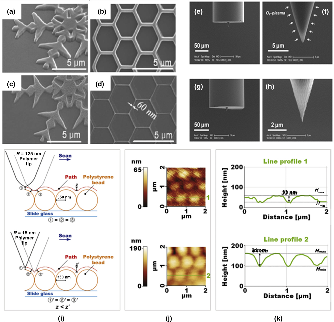
O2-ashing is a technique commonly employed for the surface treatment and cleaning of substrates, but it can also be used for a secondary process to improve the resolution of microstructures. The 2D polymer patterns fabricated by the TPS process shown in Figs. 11(a) and 11(b) underwent O2-ashing to make structures with finer features, as shown in Figs. 11(c) and 11(d). The features of the pattern become dramatically thin and sharp, with line thicknesses as small as 60 µm. These results show that O2-ashing can be used effectively as a secondary process for improving resolution and sharpening 2D and 3D polymer microstructures fabricated by TPS process.[Reference Jung, Kong, Cho, Lee, Park, Yang and Lee76] Such high-resolution patterns can be used as mastermolds in scaling up production.
SEM images of 2D polymer patterns (a) and (b) before and (c) and (d) after O2-ashing process and (e)–(h) fabricated polymer tips. (i) Schematic concept of AFM measurement and (j) obtained topographic images and (k) line profiles. Reproduced with permission from Ref. Reference Jung, Kong, Cho, Lee, Park, Yang and Lee76 (Elsevier).

The sequential TPS-O2-ashing technique was used to fabricate ultrafine tips for an atomic force microscopy (AFM) probe on the surface of an optical fiber. The optical fiber was dipped in a photoresist and the tip was fabricated on the cross-section of the tip of the optical fiber, as seen in Figs. 11(e) and 11(f). The smallest radius of curvature of a tip apex fabricated via TPS with the optimization of laser power and exposure time is approximately 125 nm, as seen in Figs. 11(e) and 11(f). By employing the O2-ashing process, the radius of curvature of a tip apex is reduced to 15 nm, as seen in Figs. 11(g) and 11(h). Because the fabrication resolution of the TPS process is larger than the radius of curvature of a conventional AFM probe tip, an AFM tip fabricated by TPS has a limitation in obtaining topographic images and line profiles of a self-assembled monolayer or 350 nm polystyrene nanobeads; top images of Figs. 11(i)–11(k). The O2-ashing process was employed to reduce the radius of curvature of the fabricated polymer tip. The AFM tips with O2-ashing gave superior topological images and line profiles, as seen in the bottom images of Figs. 11(i)–11(k). The reduction in radius of curvature of the AFM tip leads to sharper topological images and line profiles. The sharper tip leads to deeper imaging of void spaces between the beads along with better images and line profiles. The fabrication of components on the tip of optical fibers using TPS can be used to integrate optically active microstructures on to the optical fiber.[Reference Liberale, Cojoc, Candeloro, Das, Gentile, De Angelis and Di Fabrizio77, Reference Bückmann, Stenger, Kadic, Kaschke, Frölich, Kennerknecht, Eberl, Thiel and Wegener78] Due to its simplicity, this technique can be easily adapted to manufacturing. The recent emergence of dip-in TPS technology could be very suitable for large-scale interactions of fabrication on optical fibers.
Cell growth scaffolds
3D scaffolds containing single cell level (~10 µm) microenvironments are considered crucial in understanding the structure and behavior of cancerous cell growth.[Reference Kuo, Chiang, Huang, Lee and Wo79–Reference An, Choi, Lee and Choi81] The structure of cancer cells governs their proliferation and response to external stimuli such as drugs.[Reference Gottesman82] Traditional 2D culturing of cancer cells has some disadvantages in evaluating the in vivo behavior of cancer cells. Cells in 2D cultures tend to stretch out on flat culture surfaces, while the cells on 3D scaffolds adapt a spheroidal configuration more akin to in vivo cancer cells. These limitations have led to the exploration of scaffold structures facilitating 3D cultures of cells. Hierarchical 3D structures consisting of 3D arrangements of compartments capable of accommodating cells could create an ideal microenvironment for studying them.
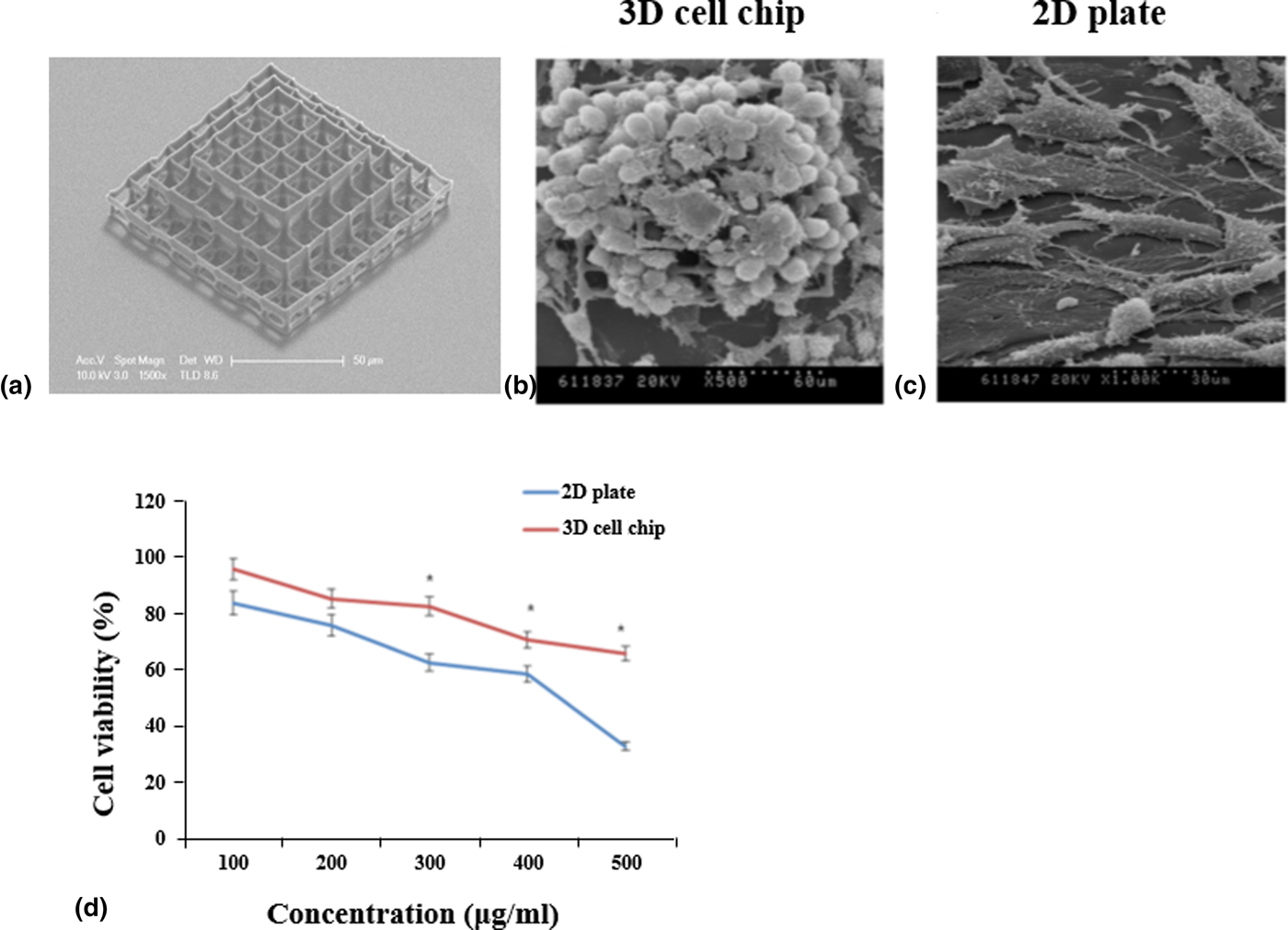
An example of a 3D cell growth scaffold fabricated by TPS can be seen in Fig. 12(a). The pyramidal array of a hierarchical structure consisted of a hexahedral structure with dimensions of 12 µm × 12 µm × 12 µm. Investigations with HeLa cells and Du145 cells revealed that the cells formed spheroidal structure aggregates when they were subjected to a 3D cell culture.[Reference Lee, An, Shin, Ha, Son, Seok and Lee83, Reference Lee, Hee An, Ha, Son, Yang, Jung, Lee and Choi84] Cells cultured in a 3D cell chip exhibited excellent cell morphology and had high cell viability. The cells cultured in traditional 2D culture plates showed a flat well spread morphology. The difference in morphology of Du145 cells cultured in 3D and 2D can be seen in the scanning electron microscopy (SEM) images in Figs. 12(b) and 12(c). Cells in vivo are surrounded by other cells as well as extra-cellular matrices. The proximity and aggregation exhibited by the cells cultured in the 3D cell chip make it closer in character to in vivo systems. The morphological differences between 3D and 2D cultured cells also affect their response to cancer drugs. The 3D cultured Du145 cells were resistant to higher dosages of the cancer drugs. A comparison between two different types of cell cultures when exposed to the drug mitoxantrone can be seen in the cell viability graph in Fig. 12(d). With a drug dose of 500 µg/ml, the viability of the 2D cultured cells decreased rapidly in comparison. Even at a low concentration of the cancer drug, the viability of the cells in the 3D culture was higher than those in the 2D culture.
(a) A 3D pyramidal structure with hexahedral compartments for 3D cell culturing. (b) 3D cultured Du145 cells. (c) 2D cultured Du145 cells. (d) Cell viability of 3D and 2D cultured cells. Reproduced with permission from Ref. Reference Lee, An, Shin, Ha, Son, Seok and Lee83 (OSA Publishing).

Summary and outlook
Two decades of nanotechnology has given us an understanding of the complexities of form and function in different nanomaterials. Biomimetic research has also reiterated the role of microstructure in defining functional properties of many natural materials. Lotus leaves, nacre, and the colors of butterfly wings are some examples of microstructures leading to unique properties. TPS provides an easy platform to fashion microstructures with a diverse set of materials such as polymers, ceramics, inorganic, and organic–inorganic hybrid materials, as demonstrated in the previous sections. The past two decades of research has evolved a very detailed understanding of two-photon absorbing materials that facilitate a high degree of control over the photoinduced processes.[Reference Lee, Kim, Yang and Park10] There is an ongoing effort to adapt TPS for mass manufacturing of microstructures. For a long time, the easiest substrates for TPS were thin transparent ones because the fabricating laser beam should pass through the substrate to reach the photoactive material. The use of opaque substrates such as silicon wafers often required complex sample setups. This has changed in recent years due to the introduction of dip-in fabrication techniques that involve the lens dipping into the photoactive medium. This approach has no substrate dependence and increases the applicability of TPS to a wide range of substrates.[Reference Ha and Yang75] Most of the structures fabricated with TPS are fixed to a substrate after fabrication where they can only be used for localized applications. The extremely small sizes of the structures fabricated by TPS make them difficult to manipulate and recover once they are lifted off the substrate. Recently introduced two-photon flow lithography attempts to overcome this issue by carrying out fabrication in a microfluidic environment and manipulating structures within a microfluidic flow.[Reference Shaw, Chizari, Shusteff, Naghsh-Nilchi, Di Carlo and Hopkins85, Reference Laza, Polo, Neves, Cingolani, Camposeo and Pisignano86] Such developments have contributed to widening the scope of TPS as a tool for designing self-assembling structures.
The scalable and fast fabrication (hundreds of millimeters to centimeters per second) of large structures on different substrates at high resolutions with good reproducibility is a pre-requisite for widespread adaptation of TPS as a manufacturing method.[Reference Shaw, Chizari, Shusteff, Naghsh-Nilchi, Di Carlo and Hopkins85] Fabrication of mesoscale structures (having overall structure sizes in the scale of millimeters with smallest features ranging in size from 5 to 100 µm) have been studied to explore the possibility of industrial-scale production of micro-optical devices. Such large feature sizes have been fabricated at a fast rate using ultrafast laser processing,[Reference Malinauskas, Žukauskas, Hasegawa, Hayasaki, Mizeikis, Buividas and Juodkazis87, Reference Wang, Wang, Chung and Yen88] with a combination of linear stage, piezo-stages, and galvano-scanner for manipulation of photoactive sample.[Reference Jonušauskas, Juodkazis and Malinauskas89, Reference Jonušauskas, Gailevičius, Baravykas, Juodkazis and Malinauskas90] There have been some attempts at scaling up the capability of TPS to create microscopic assembly lines for functional structures or large area structures suitable for scalable applications.[Reference Ricci, Nava, Zandrini, Cerullo, Raimondi and Osellame91] The scale of the largest structure that can be fabricated has also expanded in recent times, with some groups demonstrating centimeter-scale structures with the TPS process.[Reference Chu, Tan, Wang, Xu, Li, Qi and Cheng92] This a far cry from the 300 to 500 µm structures is considered large scale a decade ago. The first generation of large-scale commercial TPS systems are starting to appear on the market.[Reference Stender, Mantei and Houbertz93] To be taken seriously all nanomanufacturing technologies should content with and comply with the norms of metrology set by the semiconductor industry.[Reference Liddle and Gallatin94] A recent review about metrology in TPS demonstrates the plethora of factors to be considered when optimizing materials and protocols for application of TPS.[Reference LaFratta and Baldacchini95] Some factors to be considered include the non-linear optical response of the photoactive materials, the fidelity of the photo-formed structures with original designs, mechanical properties of the fabricated structures, and chemical stability of structures. All the above described will hasten the wider adaptation of TPS as a mature technology for fabrication of complex 3D microstructures. If so it will certainly lead to a revolution in many different fields of applied science such as MEMS devices, photonics, biotechnology, and structured materials/templates for electronics. Through decades of development in materials, optical/hardware techniques, and demonstrated applications, TPS is poised to become a powerful tool of the fourth industrial revolution.
Acknowledgments
This work was supported by the Mid-Career Researcher Program (2016R1A2B4008473) and the Basic Science Research Program (2017R1C1B5077130) through the National Research Foundation of Korea (NRF) funded by the Ministry of Education, Science and Technology.