The controlled assembly of functional nanoparticles can lead to nanostructures with tailored electromagnetic propagation. For example, integrating metallic plasmonic nanoparticles such as nanospheres and nanorods into architectures with well-designed geometries and sizes can control the plasmonic interaction of particles, leading to Fano resonance-based transparency windows.[ Reference Lassiter, Sobhani, Fan, Kundu, Capasso, Nordlander and Halas 1 ] Notably, photonic crystals, i.e., ordered arrays with different refractive indices and a periodicity of the order of light wavelength, prevent propagation of light in certain ranges of energy, termed the photonic band gap. The position of the photonic band gap can be controlled by adjusting the periodicity and effective refractive index.
Photonic crystals composed of silica nanoparticles have been widely studied with polystyrene latex (PSL) spheres as templates.[ Reference Iskandar, Abdullah, Yoden and Okuyama 2 , Reference Waterhouse and Waterland 3 ] The concept of photonic crystals can be extended to mesoscale particles, which would be of interest as active material in optical metafluids,[ Reference Urzhumov, Shvets, Fan, Capasso, Brandl and Nordlander 4 – Reference Sheikholeslami, Alaeian, Koh and Dionne 7 ] in specialized paints with tailored optical properties, or even aerosols with designed optical characteristics. Aerosol-based assembly of mesoporous particles out of silica and titania nanoparticles has been successful, as is reported in Refs. Reference Iskandar, Mikrajuddin and Okuyama8,Reference Iskandar, Nandiyanto, Yun, Hogan, Okuyama and Biswas9. In these studies, a mixture of colloidal nanoparticles and PSL template spheres in water was atomized and the surface tension of the evaporating solvent caused the hexagonally closely packed assembly of the PSL spheres with the nanoparticles filling the voids in between.[ Reference Iskandar, Mikrajuddin and Okuyama 8 – Reference Gradoń, Janeczko, Abdullah, Iskandar and Okuyama 11 ] Thermal annealing of these particles removed the PSL spheres and yielded photonic crystal mesoparticles.
The goal of this work is to integrate multifunctional plasmonic/excitonic semiconductor nanocrystals (NCs) into photonic crystal thin films and mesoparticles. Such structure should combine the photonic band gap of the photonic crystal with the excitonic behavior as well as the plasmonic response of the semiconductor NCs. We here report on photonic crystal films composed of non-thermal plasma-synthesized boron (B)-doped silicon (Si) NCs. These NCs exhibit unique optical properties of doping-induced plasmonic resonance in the IR region[ Reference Kramer, Schramke and Kortshagen 12 ] and strong excitonic absorption in the UV–visible region.[ Reference Yang, Kramer, Schramke, Hogan, Govorov and Kortshagen 13 ] They are easily dispersed in polar solvents; this makes B-doped Si NCs compatible with PSL template spheres for self-assembly. Furthermore, we demonstrate a simple aerosol self-assembly route to produce photonic crystal mesoparticles of B-doped Si NCs.
The B-doped Si NCs utilized here were synthesized in a non-thermal plasma reactor.[ Reference Mangolini, Thimsen and Kortshagen 14 , Reference Pi, Gresback, Liptak, Campbell and Kortshagen 15 ] A mixture gas flow of argon [35 standard cubic centimeters per minute (sccm)], silane (0.5 sccm) and diborane (10% in hydrogen) (0.3 sccm) was introduced into a quartz tube reactor, which corresponds to a nominal dopant fraction of ~10.7%. A radiofrequency power of 110 W at 13.56 Hz was applied to a pair of 1 cm-separated ring electrodes with the powered top electrode positioned at 3.9 cm above the downstream end of the reaction tube. The pressure in the plasma reactor was maintained at 133 Pa during particle synthesis and collection. X-ray diffraction and transmission electron microscopy measurements revealed well-crystallized Si NCs with a size about 11 nm. A colloidal mixture of B-doped Si NCs and 200 or 500 nm PSL template spheres was prepared with the concentrations of 0.04 wt% B-doped Si NCs and 0.09 wt% PSL spheres, using as solvent a mixture of dimethyl sulfoxide (DMSO) and H2O at a volume ratio between 0.3:1 and 0.02:1. Photonic crystals were first assembled by drop casting the colloidal mixture onto a Si wafer or quartz substrate followed by overnight drying at 60 °C. To fabricate an inverse opal structure, the samples were further annealed at 500 °C for 3 min. Assembly morphologies were studied with a scanning electron microscope (SEM) (JEOL 6700). Optical measurements were carried out using a surface and thin-film analysis spectroscopic ellipsometer VASE (J.A. Wollam Co., Inc) for reflectance (at a 15° incident angle) or a Cary 5000 UV/Vis/NIR Spectrophotometer (Agilent Technologies) for transmittance.
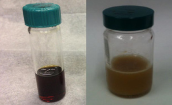
Figure 1 shows an ink of B-doped Si NCs in DMSO and a colloidal mixture of B-doped Si NCs and PSL spheres (200 nm). The B-doped Si NCs form a clear colloidal solution in DMSO; NC stability is facilitated by a Lewis acid–base interaction between surface B (acid) with the DMSO (base) solvent, following the mechanism described in Ref. Reference Wheeler, Neale, Chen and Kortshagen16.
Images of a colloidal solution of B-doped Si NCs in DMSO and a colloidal mixture of B-doped Si NCs (0.04 wt%) and PSL spheres (200 nm) (0.09 wt%) in a mixture solvent of DMSO:H2O = 0.02:1.

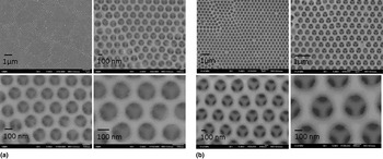
Large area self-assemblies (photonic crystals) were fabricated with the B-doped Si NCs as described above. In comparison with silica nanoparticles, the B-doped Si NCs feature strong excitonic absorption in the UV–visible regions and plasmonic resonances in the IR region of the electromagnetic spectrum. In addition, the large refractive index of Si (3.4) compared with that of silica (1.5) provides an improvement of dielectric contrast, leading to stronger photonic behavior.[ Reference Mittleman, Bertone, Jiang, Hwang and Colvin 17 , Reference Bertone, Jiang, Hwang, Mittleman and Colvin 18 ] Figure 2(a) shows SEM images of photonic crystals composed of B-doped Si NCs. They have an inverse opal structure, which was obtained after annealing the films drop-cast onto Si wafers with 200 and 500 nm PSL template spheres, respectively. The periodicity of the photonic crystals can be adjusted by changing PSL sphere size. We find 210 for 200 nm PSL spheres and 450 for 500 nm spheres, which suggest that the originally self-assembled structure collapses slightly during PSL evaporation.
SEM images of the photonic crystals of B-doped Si NCs with an inverse opal structure, which were assembled with 200 nm (a) and 500 nm (b) PSL spheres as templates. The mesoporous structure was obtained by annealing the films fabricated on Si wafers at 500 °C for 3 min.

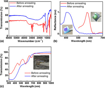
Figure 3(a) shows the Fourier transform infrared spectroscopy (FTIR) transmission spectra of the photonic crystals before and after the removal of PSL templates. Before annealing, a broad absorption band is observed in the region of 500–4000 cm−1 combined with several narrower signals. The broad absorption band is the plasmonic resonance of B-doped Si NCs. The narrow signals arise from molecular vibrations of PSL in the assembly. The feature at ~1100 cm−1 is related to Si–O–Si. After annealing, the narrow signals disappear as a result of removal of the PSL and the FTIR spectrum is dominated by the plasmonic resonance of B-doped Si NCs and an increased Si–O–Si feature.
(a) FTIR and (b) reflectance spectra of the photonic crystals of B-doped Si NCs assembled on Si wafers before and after removing the PSL spheres (200 nm). (c) Transmittance spectra of the photonic crystals of B-doped Si NCs on quartz wafer before and after removing PSL (500 nm).

The photonic band gap of a photonic crystal depends on the array periodicity and the effective refractive index. Figure 3(b) compares the reflectance spectra of the photonic crystals on Si substrates, before and after annealing treatment. Before annealing, the stop band is at 570 nm and after annealing, it blue-shifts to 420 nm. The effective refractive index and the stop band peak wavelength are determined by the following relations:[ Reference Iskandar, Abdullah, Yoden and Okuyama 2 ]
 $$\sum\limits_{n = 1}^N {\left( {{\upsilon _i}\displaystyle{{n_i^2 - n_{\rm e}^2} \over {n_i^2 + (z/2 - 1)n_{\rm e}^2}}} \right) = 0}, $$
 $$m{\lambda _{\rm p}} = 2{d_{hkl}}{(n_{\rm e}^2 - {\sin ^2}\theta )^{1/2}},$$
where N is the number of components, n i is the refractive index of the ith component, υ i is the volume fraction of the ith component, n e is the effective refractive index of the assembly, z is the number of the nearest neighbors (which is 12 for hexagonally packed architectures), m is the order of diffraction, λ p is the wavelength at the position of the stop band peak, d hkl is the spacing between the (hkl) lattice planes, and θ is the angle between the incident light and the normal to the plane. The blue-shift of the stop band is caused by the decrease of the effective refractive from 1.9 to 1.4 as a result of removing the PSL templates. Inverse opal photonic crystal films were also assembled on quartz substrates [inset in Fig. 3(c)]. There are two bands of reduced transmission in the regions of 500–700 and 300–500 nm, respectively. The first band can be attributed to the stop band of the photonic crystals. The second band has strong decrease of the transmission in the UV–visible region which is caused by the excitonic absorption of the B-doped Si NCs, which otherwise have excellent transparency in visible-to-near-IR region.[ Reference Yang, Kramer, Schramke, Hogan, Govorov and Kortshagen 13 ]
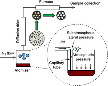
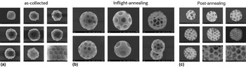
Mesocopic photonic crystal particles were produced via an aerosol processing route.[ Reference Iskandar, Mikrajuddin and Okuyama 8 , Reference Iskandar, Nandiyanto, Yun, Hogan, Okuyama and Biswas 9 ] Figure 4 depicts a schematic of the aerosol process system. A pressure driven nebulizer generates small droplets entrained in N2 carrier gas whose flow rate was 1–3 liter per minute (lpm). A silica gel diffusion drier was used to evaporate and adsorb the water. The particles were then annealed inflight in a furnace at 400 °C and then deposited by impaction on a Si wafer. We find that two factors are critical for the assembly of mesoporous particles. First, to fill the voids among the closely packed PSL template particles, the smaller Si NCs should have a diameter no larger than 0.16 times that of the templates. In our case, the ratio of the diameters of the Si NCs to PSL spheres was ~0.02–0.05. Second, the volumetric ratio of Si NCs and PSL spheres should be close to the void-to-sphere ratio of 0.35:1 in perfect hexagonally packing structure. The best results were achieved here with a volume ratio of 0.2:1 between Si NCs and PSL spheres, as the voids between the Si NCs also contribute to the infilling of the larger voids between PSL spheres. As shown in Fig. 5(a), we successfully obtained ordered, hexagonally packed mesoscopic assemblies of PSL spheres with B-doped Si NCs infilling the voids. Mesoporous photonic crystal particles shown in Figs. 5(b) and 5(c) were achieved by inflight or post-annealing treatment at 400 °C.
Schematic representation of aerosol process for making mesoscopic photonic crystal particles of B-doped Si NCs.

SEM images of the mesoscopic assemblies of hexagonally stacked PSL spheres with infilling B-doped Si NCs without (a) and with inflight (b) or post-annealing treatment (c) at 400 °C. The N2 carrier gas flow rate is 1 lpm.

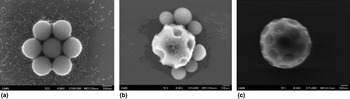
Along with the requirements for the correct particle size ratio and volume concentrations of Si NCs and PSL particles, the choice of the N2 carrier gas flow rate and DMSO concentration is important. With a DMSO:H2O ratio of 0.3:1, ordered mesoparticles can be formed at a N2 flow rate of 1 lpm. However, as indicated in Figs. 6(a) and 6(b), ordered assembly is precluded at a higher N2 flow rate of 3 lpm either with or without inflight annealing treatment. Presumably, the solvent (including DMSO) does not completely evaporate during transit through the silica drier under these conditions, and the residual DMSO will likely still disperse the B-doped Si NCs, preventing assembly of hexagonally packed structures. This finding is corroborated by the fact that reduction of the DMSO:H2O ratio to 0.02:1 again leads assembly of ordered mesoparticles, as shown in Fig. 6(c).
SEM images of the samples collected at a DMSO:H2O ratio of 0.3:1 without (a) and with inflight annealing (b), and at a ratio of 0.02:1 (c) with inflight annealing. The N2 carrier gas flow rate is 3 lpm.

In summary, photonic crystals have been assembled from plasmonic/excitonic B-doped Si NCs, taking the form of inverse opal thin films. The Si NC-based photonic crystals provide a larger dielectric contrast than the conventional crystals made with silica nanoparticles and have combined optical properties of the plasmonic/excitonic semiconductor NCs and the photonic crystal structure. They enable extended control of light propagation since excitonic, plasmonic, and photonic crystal properties can be independently tuned within certain ranges. Self-assembly of B-doped Si NCs into mesoscopic photonic crystal particles has also been achieved via a simple aerosol process. The photonic crystal nanoparticles may serve as interesting constituents for optical metafluids.
Acknowledgments
The authors are grateful to Dr. Siqin He and Vivek Rawat for help in setting up the aerosol system. This work was supported primarily by the Army Office of Research under MURI Grant W911NF-12-1-0407. Part of this work was carried out in the College of Science and Engineering Characterization Facility, University of Minnesota, which has received capital equipment funding from the NSF through the UMN MRSEC program under Award Number DMR-1420013.