Introduction
Ferroelectric materials have two nonzero spontaneous polarization states in the absence of an applied electric field. The most frequently used ferroelectric material class are perovskites with the general structure of ABO3, where A and B are cations (e.g., BaTiO3 [BTO] and PbZrxTi1–xO3 [PZT]). In PZT, the B site can be occupied by either a titanium cation or zirconium cation. Perovskites typically undergo a phase transition from a nonferroelectric cubic phase at higher temperatures to a ferroelectric tetragonal phase at lower temperatures. Figure 1a shows a PZT crystal in the tetragonal phase. It becomes clear that the smaller cation (Ti4+ or Zr4+) can have two stable positions resulting in two opposite polarization states. The blue and the green cations in Figure 1 indicate the two stable positions. Please note that the Ti4+ or the Zr4+ will occupy one of the two positions only. Therefore, the polarization of ferroelectrics can be reversed when an external electrical field greater than the coercive field E c is appliedReference Mitsui, Martienssen and Warlimont1 (Figure 1a–d). Since the polarization reversal process is purely field driven, without a sufficient applied field, the polarization will remain in the previously set direction; therefore, ferroelectricity is ideal for low-power binary nonvolatile memory having two stable states that represent “0” and “1” data (Figure 1b–c). All other known emerging nonvolatile memory concepts, such as spin torque transfer magnetic random-access memory or resistive random-access memory, require passing a current through the device. Consequently, there is limited efficiency in the writing process, since not every electron that passes through the structure will contribute to the switching effect.Reference Mikolajick and Pinnow2 The field-driven polarization reversal thus gives ferroelectrics a unique selling point for nonvolatile memories.
(a) Perovskite crystal illustrating the two potential stable positions (blue and green circles) of a central cation (e.g., Ti4+ or Zr4+ in Pb(Zr, Ti)O3). (b) Corresponding diagram of the free energy, U, as a function of the polarization, P. (c) Resulting polarization, P, as a function of the electrical field, E, for a ferroelectric capacitor indicating the pulses that need to be applied for writing and reading. The green and blue color of the hysteresis in (c) correspond to the blue and green positions of the central cation, as shown in the (a) perovskite crystal. (d) When the reading pulses are applied, a current will flow according to the previously stored state. (e) Different crystal structures detected in thin hafnium oxide films. The orthorhombic structure can be observed under conditions that are typically located between those that establish the tetragonal/cubic phase and the monoclinic phase. The green arrows indicate the possible movements of the oxygen ions between the two possible stable configurations. Note: E c+, positive coercive field; E c–, negative coercive field; P +, positive remanent polarization; P –, negative remanent polarization.

As early as 1952,Reference Buck3,Reference Anderson4 the first attempts were made to realize memories based on the ferroelectric effect in barium titanate crystals. However, to mitigate problematic issues caused by the voltages applied to currently unselected cells that are connected to the same wordline or bitline of the active cells, researchers found that a selector device, which will only be turned on if the cell is operated, needed to be added. This possibility only became available after semiconductor technology reached a certain level of maturity in the 1970s and 1980s. The resulting “1 transistor—1 ferroelectric capacitor” memory (see Figure 2a) reached the market in the early 1990s.Reference Bondurant5 This success inspired the industry, and by the end of the 1990s and early 2000s, all major memory companies had programs to develop ferroelectric random-access memories (FeRAMs). The primary aim was to achieve a device that would have similar performance and cell size to dynamic random-access memories (DRAMs), yet, at the same time, be nonvolatile. Despite some significant advances,Reference Pinnow and Mikolajick6,Reference Lee and Kim7 this goal could not be reached since scaling down the cell size was hindered by integration issues, such as high thermal budget, hydrogen sensitivity, and the unavailability of advanced deposition techniques, of the complex perovskite or layered perovskite ferroelectrics. Ultimately, the required three-dimensional (3D) integration of the capacitor became an unsolvable issueReference Koo, Seo, Kim, Shin, Lee, Baik, Lee, Lee, Bae, Lim, Yoo, Park, Kim, Han, Baik, Choi, Park and Park8,Reference Yeh, Lisker, Kalkofen and Burte9 (until the present). The technology stalled at the 130-nm process generationReference McAdams, Acklin, Blake, Du, Eliason, Fong, Kraus, Liu, Madan, Moise, Natarajan, Qian, Qiu, Remack, Rodriguez, Roscher, Seshadri and Summerfelt10 and did not follow the scaling of other technologies into the 20-nm regime available today. Therefore, the cost per bit remains high, and the technology remained limited to niche applications where the low-power write operation was an absolute must. The resulting high cost was accepted due to the absence of alternatives.
Realization of nonvolatile random-access memories (RAMs) using ferroelectric and antiferroelectric hafnium oxide. (a) Circuit diagram of conventional ferroelectric random-access memory (FeRAM), using (b) ferroelectric hafnium oxide to overcome the 3D integration challenge. (Left) Transmission electron microscope image of the cross section of 10-nm aluminum-doped hafnium oxide in a 3D structure; (right) hysteresis for the 3D structure (blue) and a planar structure having the same projected area A*B (green). The orthorhombic hafnium oxide structure in the inset of the left figure indicates the required crystal phase and is explained in Figure 1e. (b) Reprinted with permission from IEEE.Reference Müller, Böscke, Müller, Yurchuk, Polakowski, Paul, Martin, Schenk, Khullar, Kersch, Weinreich, Riedel, Seidel, Kumar, Arruda, Kalinin, Schlösser, Boschke, van Bentum, Schröder and Mikolajick68 (c) Antiferroelectric memory concept to overcome the limitations in cycle endurance and low-voltage operation. The dotted hysteresis loop shows the original antiferroelectric hysteresis. The solid hysteresis loop shows the hysteresis after it was shifted by a built-in voltage using electrodes with different work functions. The circles marked “0” and “1” on the solid hysteresis loop indicate the two states used for information storage. The tetragonal hafnium oxide structure in the inset indicates the required crystal phase and is explained in Figure 1e. Red spheres represent oxygen anions, and blue spheres represent hafnium cations; green arrows indicate the possible movements of the oxygen ions between the two possible stable configurations. Note: FE, ferroelectric; BL, bit line; WL, word line; PL, plate line; C BL, bit-line capacity; P R, remanent polarization.

Early on, another path seemed attractive. In the FeRAM described so far, a ferroelectric capacitor is used as the storage device and reading of the stored information is performed by evaluating the current response due to switching (or not switching) the capacitor with an applied voltage (see Figure 1d). The ferroelectric can instead be integrated into the gate stack of a ferroelectric field-effect transistor (FeFET) (Figure 3).Reference Ross11 The current in the device is modulated based on the polarization of the ferroelectric layer. However, this solution had additional issues. Since perovskites have a high permittivity (in the range of a few hundreds), the series connection between the ferroelectric, the interface oxide, and the depletion layer in the silicon leads to a depolarization field across the ferroelectric in the retention case were no external voltage is applied, making nonvolatility difficult to achieve.Reference Ma and Han12
Ferroelectric field-effect transistor (FeFET) as (a) a concept and (b) transmission electron microscope micrograph of the FeFET cross section realized in a 28-nm complementary metal oxide semiconductor process. The different layers in the gate stack are indicated on the right.Reference Müller, Yurchuk, Schlösser, Paul, Hoffmann, Müller, Martin, Slesazeck, Polakowski, Sundqvist, Czernohorsky, Seidel, Kücher, Boschke, Trentzsch, Gebauer, Schröder and Mikolajick53 Note: MW, memory window.

After four decades of research, nonvolatile FeFETs were demonstrated using SrBi2Ta2O9 (SBT). However, to achieve a reasonable memory window and mitigate the depolarization issue, a thick ferroelectric needed to be used, defeating the purpose of better scalability.Reference Sakai and Ilangovan13 Therefore, in the time frame from approximately 2005 to 2011, it seemed that the physical advantage of ferroelectrics for nonvolatile storage would remain restricted to niche applications such as data logging where frequent overwrites are required. Industry attention turned to other concepts based on resistive change such as magnetoresistive memories, phase-change memories, valence-change memories, or electrochemical metallization memories. It was clear that the main issue was the complexity of the ferroelectric materials (such as the one shown in Figure 1a) that could only be overcome in complementary metal oxide semiconductor (CMOS) processing under severe limitations, such as integrating oxide electrodes to solve reliability issues and hydrogen barrier layers to protect the ferroelectric from the effects of hydrogen exposure during further processing.
Ferroelectricity in hafnium oxide
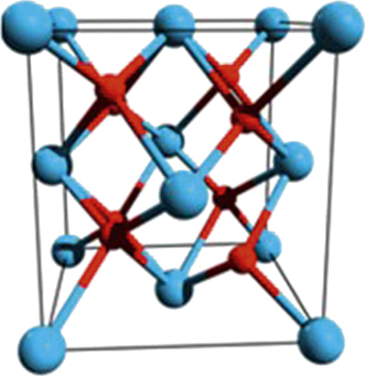
In the late 1990s, hafnium oxide became one of the most prominent high-k (k represents the dielectric constant or permittivity) materials to replace the well-established silicon dioxide in metal oxide semiconductor field-effect transistors. Hafnium oxide has reasonably high permittivity and bandgap, and is stable on silicon.Reference Robertson14 In terms of minimum leakage, the amorphous phase was preferred in transistors that became available in 2007.Reference Bohr, Chau, Ghani and Mistry15 However, crystalline phases of HfO2 (see Figure 1e) have higher permittivity than the amorphous phase. Among these, the monoclinic (space group: P21/c), the tetragonal (space group: P42/nmc), and the cubic (space group: Fm $\bar{3}$m) phases can be formed under reasonable conditions. They have permittivities of 22, 46, and 36, respectively (Figure 1e).Reference Materlik, Künneth and Kersch16 In bulk material, the monoclinic phase is the stable phase at room temperature and 1 atm, and it transforms to the tetragonal and cubic phase at 1973 and 2773 K, respectively.
The tetragonal or cubic phase induced by doping in hafnium oxide has been studied intensively. Boescke first observed a clear fingerprint of ferroelectricity in silicon doped hafnium oxide samples with doping concentrations in the few percent range.Reference Böscke, Müller, Bräuhaus, Schröder and Böttger17,Reference Böscke, Teichert, Bräuhaus, Müller, Schröder, Böttger and Mikolajick18 Since this discovery was unexpected, researchers initially used different evaluation techniques to experimentally prove that the ferroelectric hysteresis does not originate from artifacts such as leakageReference Scott19 or charge trapping. PiezoelectricityReference Martin, Müller, Schenk, Arruda, Kumar, Strelcov, Yurchuk, Müller, Pohl, Schröder, Kalinin and Mikolajick20 and pyroelectricityReference Hoffmann, Schroeder, Künneth, Kersch, Starschich, Böttger and Mikolajick21,Reference Smith, Kitahara, Rodriguez, Henry, Brumbach and Ihlefeld22 have been demonstrated as well. Additionally, it was shown that different dopants such as Si,Reference Böscke, Müller, Bräuhaus, Schröder and Böttger17 Y,Reference Mueller, Schröder, Böscke, Müller, Böttger, Wilde, Sundqvist, Lemberger, Kücher, Mikolajick and Frey23 Al,Reference Mueller, Mueller, Singh, Riedel, Sundqvist, Schroeder and Mikolajick24 Zr,Reference Müller, Böscke, Bräuhaus, Schröder, Böttger, Sundqvist, Kücher, Mikolajick and Frey25 and othersReference Schroeder, Yurchuk, Müller, Martin, Schenk, Polakowski, Adelmann, Popovici, Kalinin and Mikolajick26,Reference Xu, Shibayama, Izukashi, Nishimura, Yajima, Migita and Toriumi27 can induce ferroelectricity. Even in undoped HfO2,Reference Polakowski and Müller28 it is possible to achieve ferroelectricity by further reducing the film thickness and choosing proper processing conditions. From the beginning, it was speculated that the noncentrosymmetric orthorhombic Pca21 phase could be responsible for this behavior.Reference Böscke, Müller, Bräuhaus, Schröder and Böttger17,Reference Böscke, Teichert, Bräuhaus, Müller, Schröder, Böttger and Mikolajick18
However, with standard methods such as x-ray diffraction, a bulletproof verification of the orthorhombic phase in a mixture of monoclinic and tetragonal phases could not be achieved. Sang et al.Reference Sang, Grimley, Schenk, Schroeder and LeBeau29 used position averaged convergent beam electron diffraction analysis to prove that the orthorhombic Pca21 phase is present in ferroelectric hafnium oxide. Using this knowledge in modeling makes identification of phase fractions more convenient.Reference Park, Schenk, Fancher, Grimley, Zhou, Richter, LeBeau, Jones, Mikolajick and Schroeder30 Nonetheless, the factors leading to the formation of the orthorhombic phase are still not clear. Many factors such as stress, grain size, and doping may play a role. Materlik et al.Reference Materlik, Künneth and Kersch16 proposed that surface energy can be the most important factor, based on the fact that the gain in free energy of these factors is not sufficient to explain the stabilization of the orthorhombic phase and why the stabilization works much better in thinner films.Reference Yurchuk, Müller, Knebel, Sundqvist, Graham, Melde, Schröder and Mikolajick31 Park et al.Reference Park, Lee, Kim, Schenk, Lee, Kim, Fengler, Mikolajick, Schroeder and Hwang32 recently compared this model to experimental data in hafnium zirconium oxide. It was found that the basic experimental trends with respect to film composition confirm the model, but the best composition to achieve ferroelectric behavior is shifted to a different Hf:Zr ratio. Moreover, the observed increasing monoclinic phase fraction with increasing annealing temperature could not be explained.Reference Park, Kim, Moon, Kim, Lee, Hyun, Mikolajick, Schroeder and Hwang33 This points to the conclusion that not only thermodynamics, but also kinetic effects, need to be considered to explain the physical origin of the formation of the orthorhombic phase.Reference Park, Kim, Moon, Kim, Lee, Hyun, Mikolajick, Schroeder and Hwang33
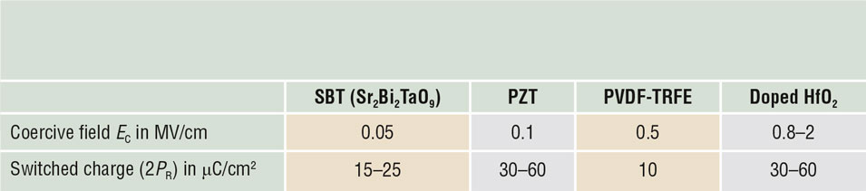
Although not all controlling parameters are understood in detail, it is now established that ferroelectricity can be reproducibly achieved in thin hafnium oxide-based films in the thickness range of 5–30 nm, thus it is suitable for further device development. As shown in Table I, ferroelectric hafnium oxide doped with various dopants has one order of magnitude higher E c and similar polarization compared to ferroelectric perovskites. E c is even higher than that of the polymer ferroelectric poly(vinylidene fluoride). Additionally, the permittivity is much lower than in perovskites, which is an important aspect in reducing the depolarization field in the FeFET.
Comparison of coercive field, E c, and switched polarization charge, 2P R, for strontium bismuth tantalate (SBT), lead zirconium titanate (PZT), poly(vinylidene fluoride):tetrafluoroethylene (PVDF-TRFE), and doped hafnium oxide.

The values given for the doped hafnium oxide span the range that have been observed using different dopants such as Si, Al, Y, La, as well as mixed crystals from Hf and Zr.
FeRAMs
The most straightforward way to realize a ferroelectric memory is to use the DRAM architecture, replacing the dielectric by a ferroelectric and pulsing the plate line instead of keeping it grounded (see Figure 2a). This modification is necessary since in the ferroelectric capacitor, compared to DRAM where the electrical field is supplied by the charged capacitor, the storage is maintained at 0 V and the capacitor needs to be actively driven via the plate line to read the stored polarization (see Figure 1d). To increase the signal, in the early days, two such cells, where one is written into the direction that should be stored (e.g., 0) and the other is written into the opposite direction (e.g., 1), were combined to realize one bit. Later, the second cell was replaced by one reference cell for a large number of cells in order to save space. The first products appeared on the market as early as 1993,Reference Bondurant5 and today, advanced products use 130-nm technology.Reference McAdams, Acklin, Blake, Du, Eliason, Fong, Kraus, Liu, Madan, Moise, Natarajan, Qian, Qiu, Remack, Rodriguez, Roscher, Seshadri and Summerfelt10 However, further success beyond niche markets is hindered by the fact that a 3D capacitor has not been practically realized using perovskite materials.Reference Koo, Seo, Kim, Shin, Lee, Baik, Lee, Lee, Bae, Lim, Yoo, Park, Kim, Han, Baik, Choi, Park and Park8,Reference Yeh, Lisker, Kalkofen and Burte9
With ferroelectric hafnium oxide, the full advantages of 3D integration can be attainedReference Polakowski, Riedel, Weinreich, Rudolf, Sundqvist, Seidel and Müller34 (see Figure 2b). However, now, the high coercive field of ferroelectric hafnium oxide is the limiting factor. On the one hand, device operation at low operating voltages is challenging. On the other hand, field cycling uses fields close to the breakdown value, limiting the device endurance with respect to the number of possible switching cycles.Reference Yurchuk, Mueller, Martin, Slesazeck, Schroeder, Mikolajick, Müller, Paul, Hoffmann, Sundqvist, Schlosser, Boschke, van Bentum and Trentzsch35 Note that due to the destructive read in the FeRAM concept, read cycles also contribute to the total number of endurance cycles. Moreover, effects like wakeup (increase in remanent polarization during the early stages of cycling) and fatigue (reduction in remanent polarization for high cycle numbers) still need to be engineered to levels as those found in perovskite ferroelectrics.Reference Schenk, Hoffmann, Ocker, Pešić, Mikolajick and Schroeder36,Reference Pešić, Fengler, Larcher, Padovani, Schenk, Grimley, Sang, LeBeau, Slesazeck, Schroeder and Mikolajick37 The issue of operating at low supply voltage can be tackled by engineering the coercive field. To date, the fabrication parameters have been observed to have only weak influence on the coercive field. An oxide thickness as low as 5 nm was fabricated with good electrical parameters.Reference Müller, Polakowski, Mueller and Mikolajick38 Attempts at further lowering the thickness were also made,Reference Chernikova, Kozodaev, Markeev, Negrov, Spiridonov, Zarubin, Bak, Buragohain, Lu, Suvorova, Gruverman and Zenkevich39 although it is challenging to verify the ferroelectricity in the case that leakage becomes dominant.Reference Schenk, Schroeder and Mikolajick40
Our understanding of endurance has also significantly progressed in the last three to four years,Reference Schroeder, Pešic, Schenk, Mulaosmanovic, Slesazeck, Ocker, Richter, Yurchuk, Khullar, Müller, Polakowski, Grimley, LeBeau, Flachowsky, Jansen, Kolodinski, van Bentum, Kersch, Künneth and Mikolajick41 though much can still be learned from the optimization of lead zirconium titanate.Reference Fengler, Pešić, Starschich, Schneller, Künneth, Böttger, Mulaosmanovic, Schenk, Park, Nigon, Muralt, Mikolajick and Schroeder42 Recently, another approach has been proposed to increase the endurance in the 1-transistor-1-capacitor (1T-1C) architecture. When stabilizing ferroelectricity in hafnium oxide by dopants with radius smaller than that of Hf and at doping concentrations higher than the optimum to achieve ferroelectricity, a pinched or antiferroelectric hysteresis is observed.Reference Böscke, Müller, Bräuhaus, Schröder and Böttger17,Reference Mueller, Mueller, Singh, Riedel, Sundqvist, Schroeder and Mikolajick24,Reference Schroeder, Yurchuk, Müller, Martin, Schenk, Polakowski, Adelmann, Popovici, Kalinin and Mikolajick26,Reference Yurchuk, Müller, Knebel, Sundqvist, Graham, Melde, Schröder and Mikolajick31 (see Figure 2c; dotted line). Specifically, in the hafnium-zirconium-oxide system, this behavior is even observed for pure zirconium oxide.Reference Müller, Böscke, Schröder, Mueller, Bräuhaus, Böttger, Frey and Mikolajick43 The cycling endurance for such a structure is much higher compared to that of the ferroelectric case.Reference Pešić, Knebel, Hoffmann, Richter, Mikolajick and Schroeder44 However, since there is no remanent polarization, P R, when the electrical field is removed, the system is not nonvolatile. Pesic et al. proposed the use of a bias field that can be generated by either electrodes with different work-function valuesReference Pešić, Knebel, Hoffmann, Richter, Mikolajick and Schroeder44,Reference Pešić, Hoffmann, Richter, Mikolajick and Schroeder45 or additional fixed charges or dipoles placed inside the dielectric stack.Reference Pešić, Hoffmann, Richter, Slesazeck, Kämpfe, Eng, Mikolajick and Schroeder46 They verified this possibility using capacitor test structures.Reference Pešić, Knebel, Hoffmann, Richter, Mikolajick and Schroeder44–Reference Pešić, Hoffmann, Richter, Slesazeck, Kämpfe, Eng, Mikolajick and Schroeder46 The advantage of this approach is that now the cycling is performed between a polarized and an unpolarized state. As a result, the apparent coercive field is cut in half, and the endurance is drastically improved. Antiferroelectric hysteresis was also observed in dielectric stacks similar to those used in state-of-the-art DRAM capacitors,Reference Pešić, Hoffmann, Richter, Mikolajick and Schroeder45 making this a possible extension of today’s DRAM technology toward a nonvolatile RAM memory.Reference Pešić, Hoffmann, Richter, Slesazeck, Schroeder and Mikolajick47 Thus, ferroelectric hafnium oxide can overcome the scaling limitation of FeRAMs since mature atomic layer deposition processes exist that allow deposition of material on high-aspect-ratio capacitors. However, the higher E c imposes additional challenges. Material engineering or an alternative approach using the antiferroelectric hysteresis are possible options to overcome these limitations. To date, no fully integrated 1T-1C FeRAM array structures have been reported and research has been mainly carried out on capacitor test structures.
FeFETs
The main issues of a 1T-1C memory cell can be overcome if the ferroelectric is integrated into the gate stack of a FeFET (Figure 3a), as explained in the Introduction section.Reference Ross11 Assuming an n-channel transistor and high enough polarization that if oriented in a way that the negative charge is close to the channel and the positive charge is close to the gate electrode, the channel will be in accumulation mode. We can also assume that if the polarization is the other way around, then the channel will be in the inversion condition. If we start in the OFF state and the gate voltage is swept to a point where the positive coercive field of the ferroelectric is reached and finally exceeded, the channel will turn on. When sweeping back beyond the point where the negative coercive field is reached, the channel will be switched OFF again. Therefore, if the positive coercive field E c+ and negative coercive field E c– (see Figure 1c) have the same absolute value E c, the memory window (MW) (the difference between the two threshold voltages of the device for the two different polarization states) is given by the difference between the voltages where the respective coercive fields are reached:Reference Miller and McWhorter48
 $$MW = 2 \cdot E_{\text{c}} \cdot d_{\text{Fe}} .$$
Here, d Fe is the thickness of the ferroelectric film.
It should be noted that Equation (1) was deduced using a simplified picture. In practice, deviations from the previously discussed assumptions and the depolarization fields discussed later need to be considered. However, the consequence that the maximum attainable memory window is limited by the coercive field holds true and is important. Hence, the high coercive field of hafnium oxide ferroelectrics is actually a benefit rather than a drawback.
Using perovskites, much thicker ferroelectric films would be needed to achieve the same memory window, which limits scalability. Only for remanent polarization of the ferroelectric that is too low to cause sufficient electrical field can we expect a significant influence of the remanent polarization on the memory window.Reference Miller and McWhorter48 Eventually, the remanent polarization will influence the effective gate overdrive of the device, and therefore, will influence the ON current.Reference Miller and McWhorter48 Because of threshold voltage shifts during polarization switching, a lower subthreshold swing, compared to a nonferroelectric transistor that has the same effective gate dielectric thickness, can be achieved. The subthreshold swing is the voltage swing that is required to change the transistor current by one order of magnitude and describes the ability to efficiently switch the transistor between the ON and OFF states. However, if the effect is not a consequence of a stabilized negative capacitance effect,Reference Salahuddin and Datta49 the polarization reversal would lead to a switching hysteresis.
In the transistor, a serial capacitor consisting of not only the capacitance of the depletion layer in the semiconductor, but also the unavoidable interface oxide between the channel and the ferroelectric, is an integral part of the structure. This series connection means the voltage that has to be applied to the device for polarization switching is increased compared to the case of a pure ferroelectric capacitor, and in the case of no applied electrical field (e.g., the case of retention), an increased internal depolarization field will be the consequence.Reference Ma and Han12 Since perovskite-based ferroelectrics have permittivity in the range of a few hundreds, a large thickness is required to balance this inherent capacitive divider. The much lower permittivity of hafnium oxide is beneficial here, and additionally, the high coercive field helps to stabilize the polarization in the retention case.Reference Gong and Ma50 Therefore, hafnium-based ferroelectrics seem to be favorable to realize FeFETs.
The first demonstrations occurred in 2011.Reference Böscke, Müller, Bräuhaus, Schröder and Böttger51,Reference Müller, Boescke, Schroder, Hoffmann, Mikolajick and Frey52 In 2012, it was verified that use of ferroelectric hafnium oxide can close the scaling gap between FeFETs and conventional FETs.Reference Müller, Yurchuk, Schlösser, Paul, Hoffmann, Müller, Martin, Slesazeck, Polakowski, Sundqvist, Czernohorsky, Seidel, Kücher, Boschke, Trentzsch, Gebauer, Schröder and Mikolajick53 Encouraged by this work, in 2016, the first fully integrated technology, where FeFET memory arrays were embedded in a 28-nm CMOS process, was demonstratedReference Trentzsch, Flachowsky, Richter, Paul, Reimer, Utess, Jansen, Mulaosmanovic, Müller, Slesazeck, Ocker, Noack, Müller, Polakowski, Schreiter, Beyer, Mikolajick and Rice54 (Figure 3b). One year later, scaling to 22-nm fully depleted silicon-on-insulator technology together with further advances in the performance of the memory arrays were shown.Reference Duenkel, Trentzsch, Richter, Moll, Fuchs, Gehring, Majer, Wittek, Müller, Melde, Mulaosmanovic, Slesazeck, Müller, Ocker, Noack, Löhr, Polakowski, Müller, Mikolajick, Höntschel, Rice, Pellerin and Beyer55
Thus, the vision of realizing nonvolatile memories based on FeFETs has moved to realization much faster than in the previous 30 years of research. However, memories are not the only application for FeFETs. Salahuddin and DattaReference Salahuddin and Datta49 proposed the concept of negative capacitance transistors in 2008 to overcome the so-called Boltzmann tyranny. This means that the subthreshold slope of FETs are limited to 60 mV/decade at room temperature, therefore, scaling of the supply voltage is limited. This concept makes use of stabilizing the ferroelectric in the negative differential capacitance region between the two stable polarization states by using a suitable dielectric capacitor in series. The negative differential capacitance region is caused by an energy barrier giving rise to a negative change in charge with changing voltage (see Figure 1b). Eventually, the stabilized negative capacitance will lead to a voltage boost on the internal node between the ferroelectric and the transistor dielectric. Consequently, a smaller subthreshold swing together with a higher ON current is possible.Reference Lin, Khan, Salahuddin and Hu56
Again, the integration challenge of combining ferroelectrics with CMOS processes needs to be overcome and ferroelectric hafnium oxide seems to be the material of choice for such devices. Initial device demonstrations have been shown,Reference Li, Chen, Lai, Lin, Cheng, Chen, Wei, Hou, Liao, Lee, Chen, Sheih, Yeh, Yang, Salahuddin and Hu57,Reference Lee, Fan, Tang, Chou, Chen, Kuo, Xie, Liu, Liao, Jong, Li, Chen and Liu58 although the issue of stabilization of the negative capacitance state remains to be resolved. As a first step, the transient negative capacitance was observed.Reference Hoffmann, Pešić, Chatterjee, Khan, Salahuddin, Slesazeck, Schroeder and Mikolajick59 However, the exact boundary conditions for stabilizing the negative capacitance operation region are still under scientific debate and need clarification.Reference Hoffmann, Pešić, Slesazeck, Schroeder and Mikolajick60–Reference Kim, Yamada, Moon, Kwon, An, Kim, Kim, Lee, Hyun, Park and Hwang62
Summary and future prospects
From a physical viewpoint, ferroelectrics are an almost ideal candidate for binary nonvolatile memories, since they have a field-driven switching mechanism. However, the complexity of the traditional perovskite materials and the resulting difficulties to integrate them into the CMOS process has hindered the fast scaling of such devices. The unexpected discovery of ferroelectricity in doped hafnium oxide has completely changed this picture, because hafnium oxide is a standard material in CMOS processing, with manufacturing processes available for different scenarios.
From an electrical parameter point of view, ferroelectric hafnium oxide differs from perovskites in having a much higher coercive field, E c, and a much lower permittivity. When using the material in the traditional 1T-1C ferroelectric RAM configuration, the high coercive field imposes challenges with respect to low-voltage operation and cycling endurance. Antiferroelectric memory has been proposed to overcome these limitations. When integrating ferroelectric hafnium oxide into the gate stack of a transistor, resulting in a FeFET, both aspects give this material a competitive edge. The developmental progress of FeFETs has significantly increased by the adoption of ferroelectric hafnium oxide.
Nevertheless, achieving a cycling endurance beyond the level of conventional charge-based nonvolatile memories remains a challenge.Reference Chernikova, Kozodaev, Markeev, Negrov, Spiridonov, Zarubin, Bak, Buragohain, Lu, Suvorova, Gruverman and Zenkevich39,Reference Yurchuk, Müller, Müller, Paul, Pešić, van Bentum, Schroeder and Mikolajick63 Different strategies have been proposed to overcome these limitationsReference Mueller, Polakowski, Muller, Mulaosmanovic, Ocker, Mikolajick, Slesazeck, Flachowsky and Trentzsch64 and encouraging results have recently been published.Reference Chatterjee, Kim, Karbasian, Tan, Yadav, Khan, Hu and Salahuddin65 The fact that differently optimized FeFETs are also an option to make steep subthreshold devices by stabilizing the negative capacitance region has further inspired the research and development of such devices. Finally, ferroelectricity is a material property that is accompanied by piezoelectricity and pyroelectricity.Reference Mitsui, Martienssen and Warlimont1,Reference Martin, Müller, Schenk, Arruda, Kumar, Strelcov, Yurchuk, Müller, Pohl, Schröder, Kalinin and Mikolajick20,Reference Smith, Kitahara, Rodriguez, Henry, Brumbach and Ihlefeld22 These properties open the path toward integrated sensors, actuators, and energy-harvesting functionalities, and these are only in the early stages of exploration.Reference Hoffmann, Schroeder, Künneth, Kersch, Starschich, Böttger and Mikolajick21,Reference Park, Kim, Kim, Moon, Kim and Hwang66,Reference Park, Schenk, Hoffmann, Knebel, Gärtner, Mikolajick and Schroeder67
Acknowledgments
The authors thank all current and former team members at NaMLab, Fraunhofer IPMS-CNT, Global Foundries, Seoul National University, and all cooperation partners for their dedicated work on ferroelectric hafnium oxide and its applications. Part of this work was supported by the EFRE Fund of the European Commission within the scope of technology development, the Free State of Saxony (Germany), and the German Research Foundation (Deutsche Forschungsgemeinschaft; Project MI 1247/11–2). M.H.P. is supported by a Humboldt Postdoctoral Fellowship from the Alexander von Humboldt Foundation.

Thomas Mikolajick has been a professor of nanoelectronic materials at Technische Universität Dresden (TU Dresden) and a scientific director of the Nanoelectronic Materials Laboratory gGmbH, Germany, since 2009. He received his Dipl-Ing degree in 1990 and his Dr-Ing degree in 1996 in electrical engineering, both from the Friedrich-Alexander-Universität Erlangen-Nürnberg, Germany. From 1996 to 2006, he worked in the semiconductor industry at Siemens, Infineon and Qimonda. In 2006, he was appointed professor of materials science of electron devices at Technische Universität Bergakademie Freiberg, Germany. Since 2009, he holds a professorship for nanoelectronic materials at TU Dresden in combination with the position of scientific director of the Nanoelectronic Materials Lab. He has authored or co-authored more than 300 publications and holds approximately 50 patents. Mikolajick can be reached by email at thomas.mikolajick@namlab.com.

Stefan Slesazeck joined the Nanoelectronic Materials Laboratory gGmbH, Germany, as senior scientist in 2009. He received his PhD degree in microelectronics from Technische Universität Dresden, Germany, in 2004. He joined Qimonda Dresden as a device engineer and studied the predevelopment of three-dimensional dynamic random-access memories (DRAMs) down to 46-nm technology and concept evaluation for 1T-DRAM. His current interests include device and concept development, electrical characterization, and modeling of memories. He is the author/co-author on more than 80 papers and holds six US patents. Slesazeck can be reached by email at stefan.slesazeck@namlab.com.

Min Hyuk Park has been a postdoctoral researcher in the Nanoelectronic Materials Laboratory gGmbH, Germany, since 2015. He received his BS degree in 2008, and his MS and PhD degrees in 2014, both in materials science and engineering from Seoul National University, South Korea. He has been supported by the Alexander von Humboldt Foundation since 2016. His research interests include ferroelectric and antiferroelectric (Hf, Zr)O2 and doped HfO2 thin films for memory, energy storage, energy harvesting, solid-state cooling, and sensor applications. He has co-authored more than 40 papers. Park can be reached by email at minhyuk.park@namlab.com.

Uwe Schroeder joined the Nanoelectronic Materials Laboratory gGmbH, Germany, in 2009. He received his PhD degree from the University of Bonn, Germany, in 1995, and subsequently, he was a postdoctoral researcher at The University of Chicago. In 1997, he joined Infineon, formerly Siemens Semiconductor, for dynamic random-access memories (DRAMs) capacitor development in the DRAM Development Alliance with IBM and Toshiba, before transferring to Infineon’s Memory Development Center, Germany, in 2000. His current research focuses on high-k dielectrics and ferroelectric HfO2 layers in semiconductor devices. He has co-authored more than 150 papers and conference contributions and holds more than 30 patents. Schroeder can be reached by email at uwe.schroeder@namlab.com.