I. INTRODUCTION
There is an increasing demand of high-efficiency antennas and passives for applications where high-frequency operation, lightweight, and conforming to a curved surface are required. Flexible electronics have spanned impressively over the past years, and flexible substrate became a strong competitor compared with his rigid counterparts because they are typically lighter, more rugged and portable, and less expensive to manufacture [Reference Wong and Salleo1].
A) Flexible substrate choice
The choice of flexible substrate for the applications at microwave frequencies is a challenge, because the substrate must exhibits good electrical (e.g. low losses), mechanical, and chemical properties. Moreover, the substrate should keep these electrical properties over a wide range of frequencies and under external conditions such as temperature and pressure, etc. Finally, the substrates used in radio frequency (RF) devices should be able to withstand the rigors (e.g. humidity and gasing) of their operating environment and of the fabrication processes used in their packaging [2].
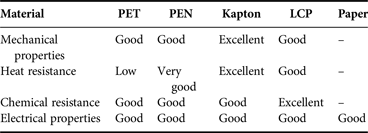
Several flexible substrates used for the printed circuit packaging are listed in Table 1; one can see the characterizations of polyethylene teraphthalate (PET) [Reference Hettak, Petosa and James3], polyethylene naphthalate (PEN) [Reference Bisognin4], Kapton (http://www.dupont.com/content/dam/assets/products-and-services/membranes-films/assets/DEC-Kapton-summary-of-properties.pdf), liquid crystal polymers (LCP) [2], and paper-based substrate [Reference Shaker, Safavi-Naeini, Sangary and Tentzeris5]. LCP has a nearly constant relative permittivity of 3.1 and low loss (tan δ = 0.002–0.005) up to millimeter wave frequency range, along with a near-hermetic nature (water absorption <0.04%) which make it suitable for high-frequency designs. The paper-based substrate is a good candidate thanks to its low cost, but it has limitations issues related to high frequency, absorption, and humidity. Finally, we selected Kapton as the substrate for the development of our passive circuits due to its good RF and thermal properties, very good flexibility over a wide temperature range (−73 to +400 °C) and its resistance to many chemical solvents.
Comparative properties of state-of-the-art flexible substrates [Reference Vyas, Rida, Bhattacharya and Tentzeris6].

B) Process technology choice
The most widespread technologies used in microfabrication are photolithography, screen printing, and inkjet printing (Fig. 1). Inkjet printing is a direct write technology which presents a low-cost advantage because the design pattern is transferred directly to the substrate and does not require masks. However, the liquid metal nanoparticles used for inkjet printing have much lower conductivity compared with the bulk conductor used for lithography [Reference Swaisaenyakorn, Young and Shkunov7, Reference Belhaj, Wei, Pallecchi, Mismer, Roch-jeune and Happy8], which can degrade the printed circuit's performances at RF and millimeter wave frequency. In addition, millimeter wave applications require high accuracy, and both screen printing and inkjet printing can only offer a highest resolution about 20 µm [Reference Singh, Haverinen, Dhagat and Jabbour9]. Antennas fabricated on Kapton at lower frequency have been reported in [Reference Ahmed, Tahir, Shamim and Cheema10, Reference Aziz, Roy, Berge, Irfanullah, Nariyal and Braaten11] using screen printing or inkjet printing, but the traditional photolithography remains the most suitable method for the microfabrication at millimeter frequency range.
Comparison of the processing steps involved in subtractive microfabrication, screen printing, and inkjet printing [Reference Chauraya12].
This paper is organized as follows. The second chapter presents a description of the fabrication process we have developed, followed in the third chapter by a study of Kapton dielectric properties using a ring resonator method. Then, a design of a 60 GHz grounded coplanar waveguide (GCPW) feeding patch antenna and two crossed-dipoles array antennas (CDAAs) at Ku band and K band are described. A prototype of crossed-slot dipole antenna (CSDA) at V band is also analyzed here. Finally, experimental results concerning the resistivity of Au bump used in flip-chip packaging is presented.
II. TECHNOLOGICAL PROCESS FOR FLEXIBLE SUBSTRATE INTEGRATION
To manufacture our circuits onto a flexible substrate, we have chosen the traditional photolithography, the main difficulty during the fabrication process lies on the flexible film handling and its use in micro-technology equipment. To overcome this difficulty, a 4 in silicon (Si) wafer is used as a host carrier. One of the critical obstacles consists in finding a way to adhere the polyimide film on the Si support. This adhesion has to be compatible with the various technological stages (vacuum, solvent, and temperature) and allows after manufacture a peeling without any physical or chemical constraint.
A matured fabrication process [Reference Jatlaoui, Dragomirescu, Charlot, Pons, Aubert and Plana13] is used where first a PolyDiMethylSiloxane (PDMS) spin coating is performed for the adhesion of the polyimide on the holding wafer. Then the Kapton polyimide is patterned on the PDMS-Si support using a Shipley 360N laminator. A resin spin coating is then realized in a fully automated resist processing tool EVG120, followed by a photolithography process (Fig. 2).
(a) Shipley 360N Laminator; (b) EVG120 resist processing system.
During the different fabrication processes, Kapton polyimide is metallized with titanium (Ti)/Au layers (50/200 nm) or Ti/copper (Cu) layers (50/500 nm) using the electron beam physical vapor deposition. In case of Cu coating, the fabrication process will be terminated with a surface finishing (gold (Au) immersion deposits) to prevent Cu from oxidizing. Both wet-etching and lift-off methods were carried out during different tests; each of them is able to obtain a sufficient resolution for the metallization tracks.
The skin depths of Au and Cu at microwave frequencies are given in Fig. 3. One can see the skin depth decrease with higher frequency. So with the metal thickness mentioned above, selected mainly for V-band applications, high losses at lower frequencies should be expected.
Skin depth versus frequency, the horizontal lines show the selected metallization thickness.
III. CHARACTERIZATION OF KAPTON
A commercially 127 µm Kapton (type 500HN) was chosen as our flexible substrate, which is the thickest product available in the HN series. In fact, there is a minimum substrate thickness that must be respected for designing an effective patch antenna in V band. This antenna is composed by a rectangular patch on the top side of the substrate and a ground plane on the back side. To avoid undesired capacitive effect and to ensure a highly efficient radiation mechanism of a patch antenna, a quick parametric study is done. It shows the influence of substrate thickness versus maximum antenna gain in HFSS simulation (http://www.ansys.com/Products/Simulation+Technology/Electronics/Signal+Integrity/ANSYS+HFSS) (Fig. 4). One can see that the thicker the substrate, the better the antenna gain, regardless its metallization layer: perfect electric conductor (PEC), Cu, or Au.
Maximum simulated antenna gain versus substrate thickness at 60 GHz.
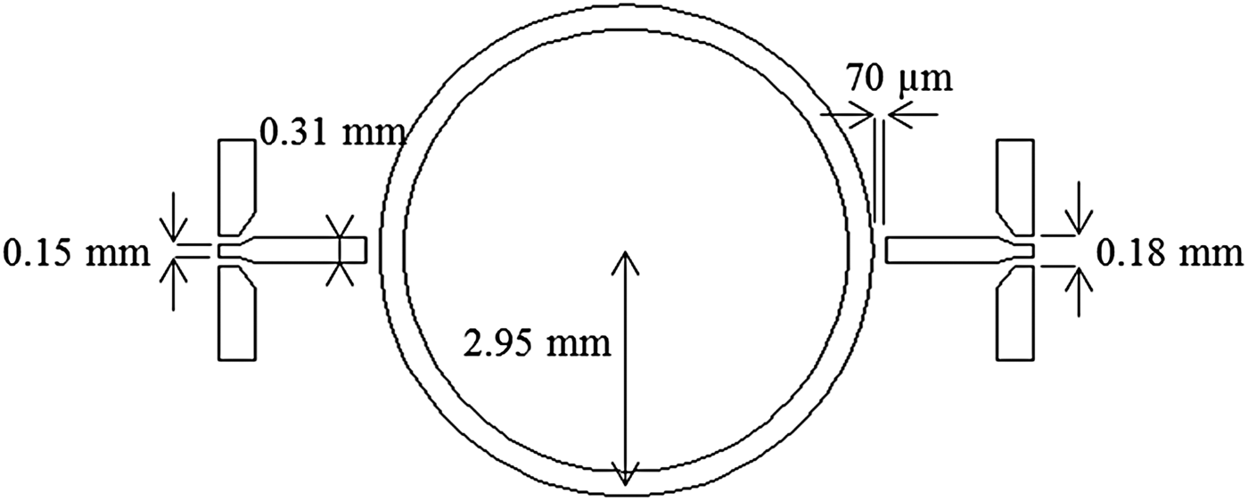
To design properly any high-frequency structure on this 127 µm Kapton using numerical simulation, the knowledge of dielectric properties of the substrate becomes necessary. The dielectric properties of Kapton: the relative permittivity ɛr and the loss tangent tan δ were extracted from S-parameters measurement of a ring resonator [Reference Thompson, Tantot, Jallageas, Ponchak, Tentzeris and Papapolymerou14]. This resonator is composed by a ring with mean radius of 2.95 mm. The width of the microstrip on the Kapton surface is 310 µm to give us characteristic impedance in the range of 50 Ω. Additionally, a GCPW to microstrip transition was optimized with the help of HFSS electromagnetic (EM) software to minimize the impedance mismatch. There are two 70 µm gaps at the edges of the ring to couple the resonator with the measurement system, which provides us sufficient coupling to measure the resonator without overload the test equipment (see Fig. 5).
Ring resonator design.
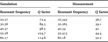
The same structures were also modeled using ADS Momentum software (http://www.keysight.com/en/pc-1887116/momentum-3d-planar-em-simulator?nid=-33748.0&cc=US&lc=eng). To fit measured and simulated data for the entire frequency band, we tuned the dielectric parameters. It is clear that the full three-dimensional (3D) finite-element method used in HFSS software is more accurate than the method of moments used in ADS Momentum, but in our case, a simulation from 10 to 65 GHz with ADS Momentum is much faster. The correlation between experimental and simulation results is depicted in Fig. 6. Simulated and measured resonant frequencies and quality factors are given in Table 2. The experimental results were obtained using an Agilent PNA network analyzer and Cascade Microtech GSG probe with a 150 µm pitch. A two-port on-wafer SOLT calibration method was used. The dielectric properties found for this Kapton polyimide are ɛ r = 3.2 ± 0.03 and tan δ = 0.012 ± 0.004 within the entire frequency band.
Simulated and measured insertion loss of the ring resonator.
Resonant frequencies and quality factors.
IV. DESIGN AND MEASEREMENT OF KAPTON-BASED PASSIVE CIRCUITS
A) Patch antenna
A 60 GHz GCPW feeding rectangular patch antenna (see Fig. 7(a)) was designed, fabricated, and measured on a flexible 127 µm thick polyimide substrate (Kapton). The GCPW-to-microstrip transition was optimized to reduce the impedance mismatch. The antenna was then characterized in terms of return loss, gain, and radiation pattern.
(a) 60 GHz GCPW feeding rectangular patch antenna; (b) measurement setup; (c) manufactured patch antenna on Kapton.
The simulated and the measured return loss of the patch antenna versus frequency are presented in Fig. 8. The agreement between experiments and simulations is very good: a relative frequency shift of only 0.7% is observed between the simulated (HFSS) and measured results. The difference is due to the uncertainties of the substrate permittivity/permeability value and under/over etching of the conductive patterns. The measured impedance bandwidth, defined by return loss less than −10 dB, is from 60.05 to 61.8 GHz (3% of relative bandwidth).
Simulated and measured return loss of the patch antenna.
The far-field radiation pattern and gain measurement were performed with a probe-based antenna measurement setup at LAAS (Fig. 7(b)). The antenna is fed through a 150-μm ground-signal-ground (GSG) probe, and this probe is directly connected to a 65 GHz VNA (Anritsu 37397D) with a flexible V-cable. Dielectric foam from Rohacell was used below the antenna to prevent reflections from the metallic part of the setup. The antenna under test was illumined by the field generated by a calibrated VT-15–25-C horn antenna from Vector Telecom.
Under these conditions, a maximum gain of 5 dBi was measured in the perpendicular direction of the antenna at 60.3 GHz. The simulated and measured radiation patterns in the H- and E-plane are given in Figs. 9 and 10. The difference of gain between simulation and measurement is about 1.7 dB, which may due to insertion loss introduced by the CPW probe and the metallization quality of conductive tracks. The E-plane radiation pattern has a restricted range due to architecture of the measurement setup because the probe was placed in the E-plane. Ripples observed in the E-plane are due to reflection and diffraction effects on the metallic micro-positioner and the probe. The 3 dB beamwidth is 56° for the H-plane.
H-plane radiation patterns of the patch antenna at 60.3 GHz.
E-plane radiation patterns of the patch antenna at 60.3 GHz.
The results demonstrate the quality of fabrication on flexible polyimide substrate and the accuracy of measurement setup for millimeter-wave antenna.
B) Crossed-dipoles array antenna
For the interest of energy harvesting for satellite health monitoring, the CDAA on Kapton polyimide is proposed, which consists of four printed half-wave dipoles arrays on the top side of the substrate. As shown in Fig. 11, CDAA is a coplanar stripline (CPS) structure. A T-junction CPS-to-microstrip was designed and optimized using intensive EM simulations to allow the excitation of the CDAA by a microstrip and the proper connection with a K “end launch” connector from Southwest for measurement purposes [Reference Takacs, Aubert, Fredon and Despoisse15].
(a) CDAA: top view of the layout (the bottom layout is represented in filled with green trellis); (b) simulation model; (c) manufactured antenna.
Two CDAAs operating in Ku and K band are fabricated and measured, respectively; their dimensions are summarized in Table 3. S-parameter measurement and simulation results are reported in Figs 12 and 13. One can see a large impedance bandwidth is obtained (measured at S 11 = −10 dB) for two proposed antennas, 15.45–19.35 GHz for the Ku band CDAA (22% of relative bandwidth), and 21.7–25.7 GHz for the K band CDAA (17% of relative bandwidth).
Simulated and measured return loss of the Ku band CDAA.
Simulated and measured return loss of the K band CDAA.
CDAA dimensions.

The radiation pattern characterizations were performed in an anechoic chamber. Figures 14 and 15 report the measured and simulated radiation patterns in two orthogonal planes at 17 GHz for the Ku band CDAA. Figures 16 and 17 report the measured and simulated radiation patterns at 22 GHz for the K band CDAA. We note that the simulation results were obtained in HFSS and the “end-launch” connector was not included in the model. The difference of gain between measurement and simulation is about 2.7 dB may due to: (i) the losses introduced by the “end-launch” connector (estimated to be in the range of 1 dB); (ii) the assembling mechanical process for connecting the Kapton structure to the connector that can lead to an imperfect contact; (iii) the skin effect. Metallization layers are composed by: (a) adherent layer of Ti about 50 nm; (b) cooper layer (thickness, 500 nm); (c) Au layer (thickness, a few nanometers). As mentioned in Section II, the skin depth of Cu at 20 GHz is 460 nm which is comparable with the total metal thickness of 600 nm; thus, unexpected RF losses may occur. The ripples observed in the YOZ plane (π = 90°) are due to reflection and diffraction effects on the connector and the coaxial cable. The 3 dB beamwidth is 52° in the XOZ plane and 65° in the YOZ plane for the Ku band CDAA at 17 GHz. For the K band CDAA, the 3 dB beamwidth is 58° in the XOZ plane and 62° in the YOZ plane at 22 GHz. As depicted from Figs 12–17, the proposed CDAAs are wideband antennas (22% of relative bandwidth in Ku band and 17% of relative bandwidth in K band). The radiation pattern do not change significantly in the relative bandwidth and the measured maximum gain is about 4.3 dBi (included the losses added by the end lunch connector and the associated mounting process and by CPS-to-microstrip T junction). We note that the gain can be increased by 3 dB if a metallic plate acting as reflector is properly putted below the CDAA.
XOZ plane (π = 0°) radiation patterns of the Ku band CDAA at 17 GHz.
YOZ plane (π = 90°) radiation patterns of the Ku band CDAA at 17 GHz.
XOZ plane (π = 0°) radiation patterns of the K band CDAA at 22 GHz.
YOZ plane (π = 90°) radiation patterns of the K band CDAA at 22 GHz.
C) Crossed-slot dipole antenna
Inspired by the design of CDAAs at Ku band and K band, and the Babinet's principle which relates the radiated field and impedance of a slot antenna to a printed (strip) antenna, a first prototype of CSDA in V band is proposed shown in Fig. 18. The antenna is designed on a 127 µm thick Kapton with a dielectric constant 3.2 and a loss tangent 0.006. CPW feed dimensions of S = 170 µm and G = 12 µm were selected corresponding to the 50 Ω GSG probe. The slot length L is fixed to 1.3 mm (quarter wavelength for 60 GHz) for the simulation, the slot width w, the stub length d, and the angle between slots α were set to 40 µm, 0.69 mm, and 45° as default, respectively.
(a) Design of CSDA; (b) simulation model.
Figure 19 shows the simulated return loss. The center frequency is 60.2 GHz, and the −10 dB bandwidth is from 58.2 to 62.05 GHz (6% of relative bandwidth). The antenna radiation patterns were also presented in Fig. 20, a peak antenna gain of 4.02 dB is obtained at 60.2 GHz.
Simulated return loss of the CSDA.
Simulated (HFSS) radiation patterns in E- and H-planes at 60.2 GHz.
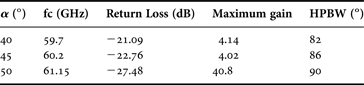
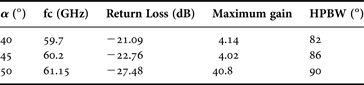
A parametric study for the angle between slots is shown in Table 4. It is seen that when the angle α increase, the peak antenna gain decrease along with a larger half-power beamwidth (HPBW) on H-plane. This phenomenon can be explained by the increase of the coupling effect when the slots approach each other.
Study of angle α effect on radiation.
As demonstrated by the simulation, CSDA has interesting performances in 60 GHz band. This antenna has no ground plane and in V band its performances (input matching and radiation pattern) can be impacted by the surrounding environment placed behind the antenna (the metallic chuck of the probe station used for S-parameters measurement or the dielectric supporting plate of the antenna setup shown in Fig. 7(b)). To avoid such issues and obtain a good correlation between simulation and measurements two solutions can be envisaged: (i) redesign this antenna using a reflector/ground plane properly positioned behind the antenna and (ii) re-simulate the antenna taking into account a representative 3D model of the surrounding environment. Both solutions are time consuming and were not implemented before the submission of this paper.
V. INTEGRATION ASSEMBLY TEST
For the purpose of integration of different components on Kapton polyimide, different dummy circuits are realized and mounted using a well-matured flip-chip technique established in LAAS-CNRS as shown in Fig. 21 [Reference Jatlaoui16]. To measure the quality of the contacts, four-probe method was used to characterize the bumps resistivity as shown in Fig. 22. A resistance about 10 mΩ was measured for the Au bump, which proves a very good DC contact has been achieved using this technique.
Description of flip-chip process.
Four-probe method resistivity measurement.
The presented Kapton supported technology can be used to develop millimeter wave circuits by heterogeneous integration for the implementation of wireless sensors network (including autonomous wireless sensors using energy harvesting or wireless power transfer techniques). The RF power used for that application is generally very low and is subject to regulation. For example in V band, the EIRP limitations for operation in the US limits (https://www.fcc.gov/document/part-15-rules-unlicensed-operation-57-64-ghz-band) the EIRP at 40 dBm (conducted power up to 27 dBm). In Europe (http://www.erodocdb.dk/docs/doc98/official/pdf/Rec0901.pdf), stipulates a maximum conducted power of less than +10 dBm. To the author best knowledge, these (maximum) authorized power levels are not critical for Kapton technology that has a very good thermal behavior.
VI. CONCLUSION
In this work, we demonstrate the feasibility of manufacturing microwave passive circuits at high frequency on a commercially available polyimide Kapton substrate through a traditional photolithography process. A 60 GHz patch antenna has been designed, fabricated, and measured to validate our technology. CDAA at Ku band and K band for energy harvesting has also been designed, fabricated, and measured. Simulation results agree well with the experimental results, only 0.7% of frequency shift is observed for return loss of 60 GHz patch antenna, 6.2 and 3.1% for Ku and K band CDAA, respectively. Future measurement for the CSDA will be carry on. The results of flip-chip test are one step further toward a heterogeneous integration on a flexible substrate of different components for autonomous wireless sensor nodes using wireless power transfer.
ACKNOWLEDGEMENTS
The authors would like to acknowledge the the CHIST-ERA project SMARTER for supporting this research work.
 Zhening Yang received his M.S. degree in communicating systems engineering from the Pierre and Marie Curie University, Paris, France in 2012. He is currently working towards his Ph.D. degree in micro/nano system for wireless communication at the LAAS-CNRS (Laboratory for Analysis and Architecture of Systems) from the Institut National des Sciences Appliquées de Toulouse (INSA Toulouse), France. His main research interests include the design, modeling and testing of RF/microwave circuits and flexible substrate heterogeneous integration for wireless communication node.
 Alexandru Takacs was born in Simleu Silvaniei, Romania, in March 1975. He received the Engineer diploma in electronic engineering from the Military Technical Academy, Bucharest, Romania, in 1999, and the Master degree and Ph. D. degree in microwave and optical communications from the National Polytechnic Institute of Toulouse, Toulouse, France, in 2000 and 2004, respectively. From 2004 to 2007, he was a Lecturer with the Military Technical Academy of Bucharest, and an Associate Researcher with the Microtechnology Institute of Bucharest. From 2008 to 2010, he occupied a Postdoctoral position with the Laboratory for Analysis and Architecture of Systems (LAAS), National Center for Scientific Research (CNRS), Toulouse, France. During 2011, he was an R&D RF Engineer with Continental Automotive SAS France, where he was in charge of antenna design and automotive electromagnetic simulation. Since 2012, he has been an Associate Professor with the University (Paul Sabatier) of Toulouse, France, where he performs research within LAAS-CNRS. He has authored or coauthored one book, one book chapter, 18 papers in refereed journals, and over 70 communications in international symposium proceedings. His research interests include the design of microwave and RF circuits, energy harvesting and wireless power transfer, small antenna design, microelectromechanical systems (MEMS) circuits and systems, electromagnetic simulation techniques and optimization methods.
Samuel Charlot was born in 1979. He received the master degree in Materials and Micro Technology from the Var Institute of technology, Toulon, France in 2004. From 2004 to 2006, he worked on the development of microfluidics systems in LAAS-CNRS, Toulouse, France. In 2006, he worked in the packaging of oxygen sensor at Néosens, Labége, France. From 2007 to 2008, he worked on a low cost technology for the integration of sensors silicon in polymer microfluidic systems in LAAS-CNRS, Toulouse, France. Since 2008, he has been working on packaging area and more specifically in screen printing technology and flip chip interconnect technology in the team packaging in LAAS-CNRS, Toulouse, France.
 Daniela Dragomirescu is Professor at the University of Toulouse (INSA Toulouse) and LAAS-CNRS laboratory. She received the engineering degree with Magna Cum Laude from the Polytechnic University of Bucarest, Romania in 1996, the MSc in circuits design from the University Paul Sabatier, France, in 1997 and the Ph.D. degree with Magna Cum Laude in 2001 from the University of Toulouse, France. Prof. Dragomirescu is the Head of Microwave and Photonics Systems Department, in LAAS-CNRS laboratory. She is the IEEE Solid States Circuits French Chapter Chair. Prof. Daniela Dragomirescu was French Government Fellow of Churchill College, University of Cambridge from February to September 2014. Prof. Dragomirescu is conducting research in the area of wireless communications with a special focus on Wireless Sensor Networks. Daniela Dragomirescu received in 2005 the French National Research Agency grant for Young Investigator which supported her in setting up the team in the Wireless Sensor Network area. She was also involved in many national and European research projects in the area of wireless communication. Daniela Dragomirescu was the coordinator of one of the nine French NanoInnov project, called Nanocomm on Reconfigurable wireless nano-sensors networks. She has published more than 70 papers in journals and conferences proceedings, 1 patent and has authored 7 academic courses.