I. INTRODUCTION
Beryllium is one of the ablator materials for use on the National Ignition Facility (NIF) due to its low x-ray opacity and high density. In particular, a graded copper-doped Be capsule is desired for ignition experiments. The capsule requires thick Be coatings (up to 160 μm), which are made on appropriate spherical mandrels, typically CH in composition.Reference Haan, Callahan, Edwards, Hammel, Ho, Jones, Lindl, Macgowan, Marinak, Munro, Pollaine, Salmonson, Spears and Suter1 The coating has to be carried out at low temperatures to avoid any deformation of the mandrel to produce uniform wall thickness and smooth and spherical surface finish. The coating must be dense with low void fraction and be leak-free when filled with D2 fuel gas. DC magnetron sputtering is used to produce the coating because of the energetics of the depositing species and relative low coating temperatures.Reference Mceachern, Alford, Cook, Makowcki and Wallace2
The coating process has been described previously.Reference Mceachern, Alford, Cook, Makowcki and Wallace2–Reference Nikroo, Xu, Moreno, Youngblood, Cooley, Alford, Letts and Cook5 Typically, Be coatings on a spherical surface show a consistent columnar microstructure with acceptable void content and size. However, the Be coatings suffer from sufficient interconnected porosity leading to rapid gas leakage. Measurements of D2 leak half-life at low temperature and ambient temperature indicate the leak is molecular flow through nanochannels.Reference Nikroo, Xu, Moreno, Youngblood, Cooley, Alford, Letts and Cook5 This points to the challenge of making thick coating on spherical surface at lower temperatures, where the sputtered Be atoms after landing on the surface will not have sufficient energy to overcome the diffusion barrier to fill all the voids. It has been documented in the literature that angled deposition can produce sculptured coating of extreme porosity.Reference Robbie and Brett6, Reference Dalla Torre, Gilmer, Windt, Kalyanaraman, Baumann, O’Sullivan, Sapjeta, Diaz de la Rubia and Djafari Rouhani7 Less diffusion and atomic shadowing are the dominant growth mechanisms of sculptured coatings. When a thin film is deposited under conditions of low adatom mobility (e.g., high melting point materials deposited onto room temperature substrates), a columnar microstructure will be produced according to Thornton’s zone theory.Reference Thornton8 This happens because atomic shadowing creates areas that incoming flux can reach, and the adatom mobility is too low to fill the voids. It has been shown in the literature that the film surface roughness increases with the increase of tilting angles of the coating while the film density decreases with the increase of tilting angles.Reference Dalla Torre, Gilmer, Windt, Kalyanaraman, Baumann, O’Sullivan, Sapjeta, Diaz de la Rubia and Djafari Rouhani7
Ion-assisted physical vapor deposition (IPVD) is the most commonly used method to produce dense films and to coat high aspect ratio trenches.Reference Helmersson, Lattemann, Bohlmark, Ehiasarian and Gudmudsson9–Reference Arunachalam, Rauf, Coronell and Ventzek13 Magnetron sputtering involves a large number of ions from the discharge. However, inert sputtering gas ions dominate, and the ions of the sputtered materials are rare. It has been demonstrated that introduction of a secondary discharge, inductively coupled plasma magnetron sputtering can achieve a high degree of ionization of the sputtered atoms,Reference Tao, Mao and Hopwood10, Reference Hopwood11 which can be accelerated toward the substrate by biasing the substrate. Using IPVD for growth of thin films has led to improved microstructures, improved adhesion, and improved coverage of three-dimensional substrates. Therefore, IPVD is a suitable approach to achieve high-density coatings on spherical substrates used for making NIF capsules. IPVD similar to that described in the literature has been used here to produce Be coatings of NIF capsules, and improved coating microstructure has been achieved.
Deposited films with large residual stress can experience deformation, cracking, and delamination. Because of the requirements of sphericity and surface roughness of Be coating on spherical substrates for NIF targets, it is essential to understand the evolution of the stress during the coating of thick Be films. For high surface mobility films that grow by the Volmer–Weber mechanism, film stress typically goes through compressive, tensile, and compressive stages. The initial compressive stress has been attributed to the nucleation of the adatoms and the interaction of adatoms with the substrate surface or the surface of the film islands.Reference Chason, Sheldon, Freund, Floro and Hearne14, Reference Friesen and Thompson15 The tensile stress following the compressive stress has been attributed to island coalescence and the formation of grain boundaries. For growth of continuous films, the incorporation of adatoms into grain boundaries is one of the mechanisms leading to compressive stress.Reference Chason, Sheldon, Freund, Floro and Hearne14, Reference Sheldon, Lau and Rajamani16, Reference Seel and Thompson17 Detor et al.Reference Detor, Hodge, Chason, Wang, Xu, Conyers, Nikroo and Hamza18 recently studied Be film stress evolution in magnetron sputtering and qualitatively modeled the transition between compressive and tensile stress. By equating the total energy the film received during sputter coating to a critical energy, the compressive and tensile region boundary can be defined, which indicates that compressive stress is due to more energy incorporation into the growing films.
II. EXPERIMENTAL PROCEDURES
Beryllium coatings were prepared in a vacuum chamber with a size of 24-inch cube pumped by a cryopump. The base pressure was typically low 10−6 to middle 10−7torr. For coating on spherical mandrels, a bounce pan is used so that the spherical substrates can be agitated during the coating for better uniformity. Be coating was produced by DC magnetron sputtering of Be targets onto ∼2-mm-diameter glow discharge polymer spheres (mainly CH) in 5–10 mTorr Ar environment. The distance between substrate and magnetron is ∼90 mm, which is not close enough to cause overheating of the substrate. Beryllium coating was deposited using three 50.8-mm-diameter targets, positioned symmetrically about the center of the chamber, operated at 100 W.Reference Xu, Nikroo, Wall, Doerner, Baldwin and Yu3, Reference Xu, Alford, Cooley, Dixon, Hackenberg, Letts, Moreno, Nikroo, Wall and Youngblood4 The substrate was grounded in reference to chamber wall except for the biasing experiments where a negative potential was applied. During the biasing experiments, a +44 V DC potential was also supplied to a 51-mm-diameter stainless steel ring located ∼6 mm above the substrate to form a secondary plasma near the film surface. The power absorbed by the DC ring is typically 20–40 W. This procedure supplies an extra flux of energized ions to the growing film surface. The details of this ion-assisted DC magnetron sputtering process have been described elsewhere.Reference Detor, Hodge, Chason, Wang, Xu, Conyers, Nikroo and Hamza18
The Be coatings were examined for leakage of D2 fuel gas by introducing the sealed Be shells into mass spectrometer (MS) after removal of the mandrel and filling with D2. The MS has been used previously for the measurement of half-lives of minutes to weeks.Reference Alfonso, Jaquez and Nikroo19 If the half-life is longer than a few weeks, the MS signal is so low that it cannot be distinguished from the background noise. The detailed procedures have been described in another publication.Reference Nikroo, Xu, Moreno, Youngblood, Cooley, Alford, Letts and Cook5
The cross section of fractured Be coatings was examined by scanning electron microscope (SEM). The detailed microstructures were analyzed by focused ion beam lift and transmission electron microscopy (TEM) imaging at the Lawrence Livermore National Lab. Because TEM only provides local void and defect information, ultrasmall angle x-ray scattering (USAXS) was used to analyze the defects or voids in the coating on a larger scale. The USAXS experiments were carried out at sector 33 of advanced photon source (APS) (Chicago, IL), with the beam energy of 12 keV. The scattering factor q is given by (4π/λ)sin θ, where λ is the synchrotron wavelength and 2θ the scattering angle. The end station consists of a Bonse–Hart camera, which can measure scattering vectors (q) from about 10−4–100 Å−1. Data were processed using the codes developed for use on this USAXS instrument and included absolute scattering intensity calibration and slit desmearing. The maximum entropy method, implemented in the “Irena” package for SAS data analysis, was used to determine scatter size distributions.Reference Ilavsky and Jemian20
Most studies of film stress in the literature focus on the initial stress development dealing with adatom nucleation and island coalescence. Typical film thickness studied is very thin compared to Be film thickness studied here. Residual stress measurements were performed in situ on flat Si substrates using a multibeam optical sensor (MOSS) system manufactured by k-Space Associates, Inc. (Ann Arbor, MI). This system uses an array of parallel laser beams reflecting from the growing substrate surface to measure surface curvature and then convert the measured curvature to the stress integrated over the sample thickness (stress-thickness) using the Stoney formulaReference Freund and Suresh21. The Si substrate has a thickness of 500 μm to ensure accurate measurements. The substrate temperature was monitored during MOSS measurements to make sure that the stress measured is mainly due to intrinsic growth stress.Reference Detor, Hodge, Chason, Wang, Xu, Conyers, Nikroo and Hamza18
III. RESULTS
A. Half-life results
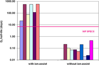
The D2 leakage half-lives of Be coatings were tested on Be shells whose mandrels were removed.Reference Nikroo, Xu, Moreno, Youngblood, Cooley, Alford, Letts and Cook5 D2 levels measured by MS of sealed Be shells were converted into half-lives. Figure 1 shows half-lives of DC magnetron and ion-assisted DC magnetron sputtering prepared Be shells. Each column represents a measurement of a Be shell half-life. Be shells are required to meet the NIF specification of a 7-day D2 half-life. The ion-assisted DC magnetron sputtered Be shells all showed longer half-lives than required and therefore meet the NIF specification. DC magnetron sputtered Be shells showed half-lives from a few minutes to a day, which are significantly shorter than the NIF specification. The half-life measurements suggested that ion-assisted DC magnetron sputtered Be coatings are leak-free for D2 gas compared to DC magnetron sputtered Be coatings.
A comparison of D2 half-lives of Be coatings produced by regular magnetron sputtering and ion-assisted physical vapor deposition (IPVD). Each column represents a measurement of a Be shell half-life.

B. SEM/TEM results
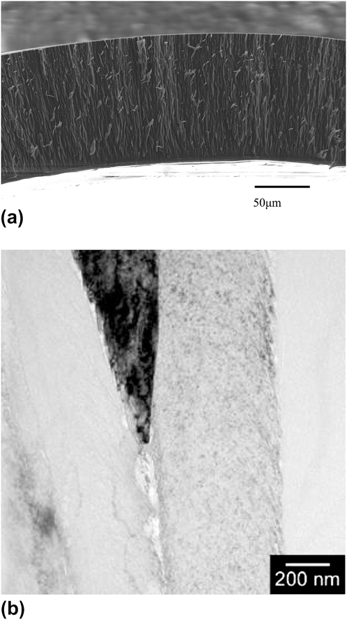
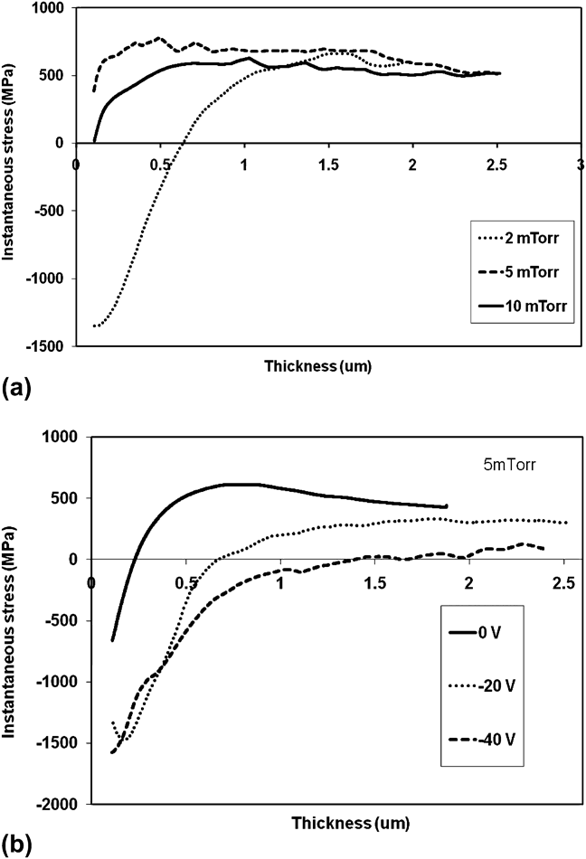
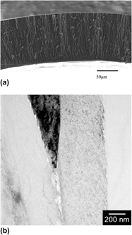
A typical Be coating prepared using DC magnetron sputtering shows columnar grain structure, as shown in Fig. 2(a). The temperature of the substrate during the coating rises to ∼150 °C. Since melting temperature of Be is 1287 °C, according to Thornton zone model the coating structure is consistent with a transition zone microstructure. In this zone, the adatoms do not have enough mobility on the surface for long-range migration and the shadowing effect leads to columnar structure. The TEM picture in Fig. 2(b) shows in high resolution the microstructure of the coating. Some voids are clearly visible along the grain boundaries. These voids are acceptable in size for NIF targets. However, coatings prepared in this way leak D2 fuel gas.
(a) scanning electron microscope cross section of a Be coating made by magnetron sputtering. The coating showed columnar grain structure. (b) A local transmission electron microscopy (TEM) picture of the coating showing voids along the grain boundaries.
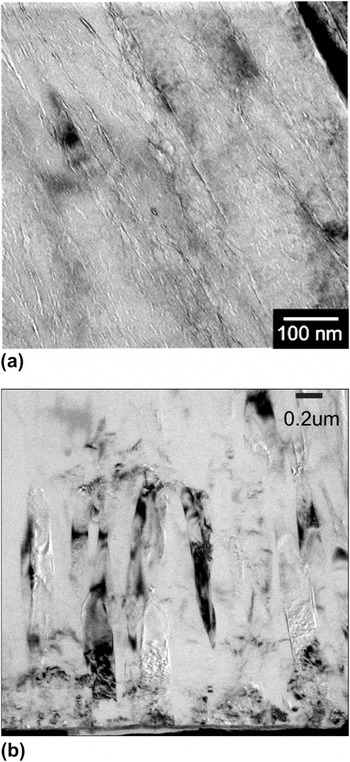
The studies of leak rates at different temperatures indicate that the leak is consistent with molecular flow mechanism and possibly through nanochannels. Detailed TEM images at high resolution reveal that there exist intragranular channels. Figure 3(a) shows a TEM image with striking features of intragranular striation lines. These striation lines are oriented along the growth direction and have a width of a few nanometers. They are believed to lead to the leakage of D2 gas. As suggested in the literatures, these channels are the result of low surface adatom mobility and shadowing effects. Since IPVD can enhance the adatom mobility by supplying more energy to the growing film, it has been used to improve the microstructure and produce leak-free Be coatings. Figure 3(b) shows a high-resolution TEM image of Be coating produced by ion-assisted magnetron sputtering method. The biasing on the substrate in this case is −80 V. It is clear from the picture that the striation line defects observed in Fig. 3(a) disappeared. This result is consistent with leak testing results that ion-assisted DC magnetron sputtering produced Be films can hold the D2 gas.
(a) High-resolution TEM images of regular magnetron sputtered Be film showing intragranular striation lines of defects. (b) An IPVD produced Be coating showed no striation line defects.

C. USAXS measurements
Although TEM characterization reveals the microscopic defects, it is limited to very localized regions of the sample. USAXS measurements can provide information on defects size and distribution on a larger scale. USAXS data were collected at 12 kV, and the beam spot size is 200 μm × 200 μm. By measuring the x-ray scattering intensity at different scattering vector q, the scatter size and distribution can be calculated. The typical magnetron sputtered Be shells showed a void fraction of 5–7% of the coating by USAXS measurement, which is consistent with previous measurements of Be coating density of 95 ± 2% by weighing.Reference Xu, Nikroo, Wall, Doerner, Baldwin and Yu3
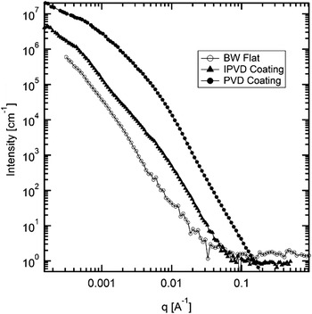
A comparison of DC magnetron sputtered Be coating with ion-assisted DC magnetron sputtered (IPVD) coating indicated reduction of void size and volume in the ion-assisted DC magnetron sputtered coatings. Figure 4 shows a comparison of two different Be capsules. One has a coating produced by ion-assisted DC magnetron sputtering and is leak-free. The other is produced by DC magnetron sputtering and leaks. A rolled Be sheet produced by Brush Wellman (Elmore, OH) was also measured as a reference, which is considered as a highly dense material. It shows that the ion-assisted DC magnetron sputtering prepared Be capsule scattering intensity is significantly reduced compared to DC magnetron sputtered Be capsule. The ion-assisted DC magnetron sputtered Be capsule scattering curve is slightly above Brush Wellman Be sheet in terms of void scattering intensity. The lower void fraction and size by ion-assisted DC magnetron sputtering compared to DC magnetron sputtering is also consistent with above TEM observations.
USXAS data comparison of Be coatings produced by IPVD method (leak-free) and by regular magnetron sputtering (leaked). Reduced scattering intensity is observed for IPVD sample. The third curve is from a flat Be sheet from Brush Wellman as a reference.

D. In situ stress measurements
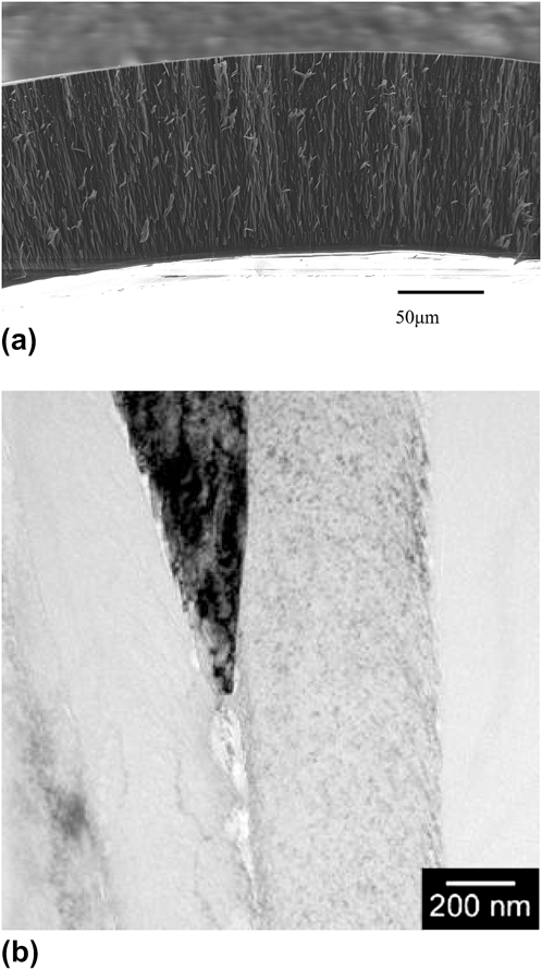
In situ stress measurements using a MOSS system were carried out on flat Si substrates during the coating to gain insight into the stress evolution with thickness. The MOSS measurements of multiple laser beam reflection spot spacing are converted to substrate curvature and then stress-thickness. Figure 5(a) shows plots of instantaneous stress at different Ar pressures. The instantaneous stress is calculated by differentiating the normal stress-thickness versus thickness curve. It represents the increment of stress contributed to the specimen at a particular thickness. It shows that after an initial rise to a tensile value the stresses at 2, 5, and 10 mTorr reach a plateau indicating that additional coating does not cause further increase of the stress magnitude. Stress recorded up to 18 μm showed the same saturation behavior. For the sample grown at 2 mtorr Ar pressure, the sputtered material initially showed more compressive stress before saturating.
(a) In situ instantaneous stress curve for Be coating at 2, 5, and 10 m Torr Ar pressures. The stress saturation was observed at larger thickness. (b) Instantaneous IPVD Be film stress curves measured by in situ MOSS. The IPVD coating under −20 and −40 V biasing showed more compressive stress than regular magnetron sputtering.
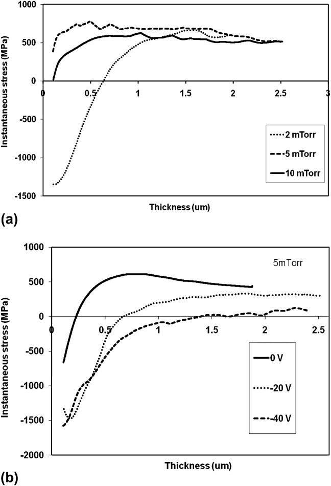
Ion-assisted DC magnetron sputtered Be coating stress was also measured by in situ MOSS. As shown in Fig. 5(b), ion-assisted DC magnetron sputtering at –20 and –40 V substrate biasing both showed more compressive stress than DC magnetron sputtering when they were measured at 5 m Torr Ar pressure. The instantaneous stress curves showed that the stress at –20 and –40 V substrate biasing approached a plateau and settled at lower stress level than DC magnetron sputtering. The compressive stress under ion-assisted DC magnetron sputtering has been discussed by Detor et al.Reference Detor, Hodge, Chason, Wang, Xu, Conyers, Nikroo and Hamza18 and was attributed to ion peening effects. The ions with sufficient energy can displace the coating surface atoms and induce atomic rearrangement and compressive stress in the growing film.
IV. DISCUSSION
Thick Be films produced by ion-assisted DC magnetron sputtering showed improved microstructure and are leak-free with respect to D2 gas. It has been discussed in the literature that metal species may be ionized in magnetron IPVD process and accelerated to the substrate by biasing the substrate. The fraction of ionized species varied from a few percent up to 30–40% of the total ion density depending on the pressure and sputtered target materials has been reported for radio frequency induced ionization.Reference Okimura and Nakamura22, Reference Rossnagel and Hopwood23 Simulation of Ta coating by magnetron sputtering suggested that atomic displacement by energetic particles during sputtering has a dramatic effect on the microstructure and morphology of the film. Without these displacements, the film density is too low. It further points out that Ta is more effective in leading to thermal diffusion because of the higher energy transfer (kinetic energy plus latent heat), while Ar energy transfer is very inefficient. The maximum kinetic energy T m that can be transferred by a projectile to a target initially at rest is given by
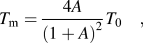
with A = m 2/m 1, T 0 is the initial kinetic energy of the projectile, m 1 is its mass, and m 2 is the target atom mass. For Ar on Be surface, the ratio before T 0 is 0.6, which means only 60% of the Ar energy can be transferred to the substrate. Be will transfer all its kinetic energy and its latent heat energy to the substrate. The latent heat energy for Be is ∼35.2 MJ/kg, which is roughly ∼3 eV.Reference Aquaro and DiPrinzio24 Under biasing conditions, the kinetic energy is e(Vbias − Vplasma). Therefore, Be ions have more energy to promote adatom surface diffusion. Ar has a relatively weak effect on film microstructure when compared to Be. Therefore, the ionized Be species in IPVD are playing an important role here to modify the coating microstructures. Since Be and Ar ionization energies are 9.3 and 15.7 eV, respectively, Be is considered more favorable to ionize compared to Ar. The measurements of ionized Be in the ion flux in this DC ring induced ionization will be discussed in future publications.
Ion-assisted DC magnetron sputtering coating has been found to produce more compressive coating due to ion peening effects. However, the stress versus thickness showed the stress still will turn to tensile after certain thickness, similar to the trend of DC magnetron sputtering. This suggests that tensile stress mechanisms, such as island coalescence, still dominate in thick Be films for both ion-assisted DC magnetron and DC magnetron sputtering. Simulations suggest that the onset of roughening during growth can inhibit the insertion of atoms into grain boundary and also contribute to the transition from compressive to tensile stress.Reference Zepeda-Ruiz, Chason, Gilmer, Wang, Xu, Nikroo and Hamza25 IPVD also leads to preferred crystal orientation for the coating. DC magnetron Be coating showed preferred orientation of (002) plane, while ion-assisted DC magnetron sputtering coating showed preferred orientation of (101) plane. This is correlated with increased surface mobility of adatoms by IPVD. (101) plane forms with a smoother and denser surface as compared to (002) plane.Reference Detor, Hodge, Chason, Wang, Xu, Conyers, Nikroo and Hamza18 We have measured that heating the substrate during DC magnetron sputtering can also lead to increased compressive stress, which is similar to ion-assisted DC magnetron sputtering. However, the heated coating does not show preferred crystal orientation of (101) plane. This suggests that IPVD and heating the substrate are different.
V. CONCLUSION
Thick Be coatings have been produced by DC magnetron sputtering. Although the void size and fraction meets the NIF target requirements, Be coatings leak D2 fuel gas. The ion-assisted DC magnetron sputtering has been demonstrated to produce leak-free Be coatings with improved microstructure. Reduced void fraction in ion-assisted DC magnetron sputtered Be coatings has been observed by TEM and USAXS measurements. The stress measurements of the coating by in situ MOSS were carried out at different pressures and substrate biases. The stress versus thickness curve showed stress saturation at larger thickness. The ion-assisted DC magnetron sputtered coatings are more compressive although they exhibit the same saturation behavior compared to DC magnetron sputtering.
ACKNOWLEDGMENTS
This work was supported by U.S. DOE under contract DE-AC52-06NA27279. Authors would like to acknowledge J. Ilavsky for the USAXS experiments and the APS, which was supported by the U.S. Department of Energy under Contract DE-AC02-06CH11357.