I. INTRODUCTION
Effective product tracking is crucial for organizations to attain suitable process efficiencies in the tough global trading competition. The industries’ product identification requirements were sufficiently satisfied through barcode systems in previous decades. Key benefits of barcodes as an optical-based technology are their proven functionality in industries as well as very low tag cost. However, it appears that barcodes are no longer capable of satisfying the market demand effectively due to their technical limitations. Low data capacity, clear line-of-sight (LoS) operation necessity, and human intervention are the major downsides of barcodes [Reference Arendarenko1]. Radio Frequency Identification (RFID) system has overcome these limitations and appealed many organizations as an effective tagging technology to fulfill current main stream demands [Reference White, Gardiner, Prabhakar and Razak2].
There are various types of RFID systems; each is suitable for specific application(s) [Reference Turcu3]. The most important classification of RFID systems is based on how their tag is powered. Mainly, tags are categorized as active, semiactive, and passive [Reference Preradovic and Karmakar4]. Active RFID tags have an on-board battery as the power supply unit. The battery power is used for signal processing purpose as well as to amplify the signal and then transmit data back to the reader. This provides a high data encoding capability for the active tags in addition to their long reading range up to 100 m [5, Reference Insider6]. Semiactive tags are also equipped with a power supply unit; however, the energy is only used for signal-processing purpose and not for signal amplifying. Hence, shorter reading range is expected; while they benefit from longer battery lifetime. There is no any on-board battery at passive tags; hence, they only rely on the transmitted power by the reader and consequently reading range of up to few meters is feasible with these passive systems [7, Reference Preradovic and Karmakar8]. The interrogation power through reader may be used to activate an integrated circuit for signal-processing purpose.
RFID systems can also be categorized in terms of their operating frequencies that are ranging from kHz to mm-wave band. Typically, low-frequency (LF) RFID systems operate at 125 kHz, although there are some that operate at 134 kHz. The band 13.56 MHz is normally used for high-frequency (HF) RFID systems. The ultrahigh-frequency (UHF) RFID systems use the band 860–960 MHz; while mostly are operating in between 900 and 915 MHz. However, there are UHF RFID applications in 433 MHz band as well [5]. There are multiple suggested bands for super high-frequency (SHF) RFID systems, including the band 2.4, 5.8, 3–10, 24–27, and 57–64 GHz [5, Reference Lu, Feng and Li9–Reference Kalansuriya, Karmakar and Viterbo11]. Based on the frequency of operation and the utilized reading technique, the tag may be located in the near-field of the reader antenna or it may fall in the far-field zone. In the near-field systems, the inductive coupling between the reader antenna (coil) and the tag is the way of wireless contact between two parts while in the far-field systems, the wave propagates between two portions and the data are transferred.
Another main categorization of RFID systems is originated from the fact that the salient features of RFID systems on providing high content capacity, long reading range, secure communication, and automatic reading process aren't sufficient enough for full replacement of barcodes [Reference Preradovic12, Reference Harrop13]. The main bottleneck of RFID systems for mass deployment is their higher tag cost. Among the three introduced categories of RFID tags, passive tags are appeared as the only option for RFID systems for the tag cost of barcode level. However, the requirement of every passive RFID tag to a silicon chip prevents RFID systems to meet the industries’ tag cost expectation [Reference Harrop and Das14]. Irrespective of huge research investment in low-cost silicon chip development, the microchip is still too expensive to be part of every RFID tag for low-cost item tagging [Reference Preradovic and Karmakar8, Reference Harrop and Das14]. Therefore, potentially the largest applications of RFID systems, which require the tag cost of below one cent (1¢) including the cost of fitting the tags in place, will not be addressed by the chipped RFID technology [Reference Harrop and Das14]. Deletion of silicon chip from a passive tag makes the tag chipless; a new category of RFID systems. Chipless tags appear to be an unavoidable approach for commercialization of RFID systems in major applications with billions of yearly taged requirements [Reference Harrop13]. Chipless RFID systems have recently attract many research interests globally [Reference Preradovic and Karmakar8, Reference Harrop and Das14, Reference Turcu15].
The conventional techniques in chipless RFID systems are presented. It is discussed that the current techniques and approaches are not successful to address the industry requirements irrespective of their satisfactory results in research phase. The idea of using the tag's electromagnetic (EM)-image for data encoding purpose has been proposed by authors [Reference Zomorrodi and Karmakar16, Reference Zomorrodi and Karmakar17]. In the previous articles, the idea of using miniaturized EM-polarizers was suggested along with some results. The main goal of this article is to: (i) expand the idea of EM-imaging and reveal more technical details; (ii) highlight the technical and practical reasons for working at mm-band 60 GHz irrespective of its vulnerability to high loss and attenuation; (iii) present some salient aspects of the proposed system in terms of secure identification and bending effect; and (iv) more details about the synthetic aperture radar (SAR)-based signal processing. Finally, the proven data encoding capacity of 2 bits/cm2 along with interesting features of the proposed technique with reasonable hardware complexity would be very attractive specifically based on a fully printable tag structure.
The rest of this communication is organized as follows: Section II introduces the conventional chipless RFID systems. Section III describes the imaging technique for data encoding purpose. Section IV proposes the appropriate data-encoding algorithm based on the technical and operational limitations. Section V shows some of the salient attributes of the techniques. General information about the SAR-based signal processing is discussed in Section VI along with final image of the tag. Section VII concludes the article.
II. CONVENTIONAL CHIPLESS RFID TECHNIQUES
The EM-waves are utilized to provide communication between the RFID reader and the tag. For the RFID chipless systems, the tag is not equipped with any processor unit; hence, the data processing is performed in the reader, while the passive tag encodes the data. In a chipless RFID system, the reader receives the tag's backscattered signal and processes it in different domains to retrieve its encoded data. This leads to the time-domain and frequency-domain-based systems [Reference Aminul Islam and Karmakar10, Reference Bhuiyan, Azim and Karmakar18, Reference Balbin and Karmakar19].
In a time-domain-based system, the reader interrogates the tag with a series of pulses [Reference Ramos, Lazaro, Girbau and Villarino20, Reference Lu, Rodriguez, Tenhunen and Li-Rong21]. The tag then re-transmits the signal as a train of echoes with some time delays with the data encoded in the delayed responses. Manipulation of the delays can be handled directly on the EM-waves, or it is possible to convert the EM-wave to another type of wave, acoustic wave for example. When a different wave type other than the EM-wave is used, then extra elements are needed for conversion [Reference Plessky and Reindl22]. For example, the inter-digital transducer element and a piezoelectric element are required in the surface acoustic wave (SAW) technique. These extra elements and their non-printable production process increase the SAW tag expense to normally higher than that of many chip-based tags. Avoiding the conversion of EM-waves to other wave types, the tag may operate on the time-domain reflectometry (TDR) principle. The TDR tag normally consists of different types of transmission lines with multiple discontinuities to create reflections in the passing signal as the encoding technique [Reference Ramos, Lazaro, Girbau and Villarino20, Reference Lu, Rodriguez, Tenhunen and Li-Rong21]. Regardless of the planar structure of the tag and possibility of direct printing, there are some basic limitations in this approach. Considering the much higher speed of EM-waves than mechanical/acoustic waves, the required circuit length is remarkably large to create detectable delays in the backscattered signal. For example, almost an 80 × 30 mm2 board size is required to encode only 4-bits of data, with the tag size rapidly increased with a higher amount of data [Reference Lu, Rodriguez, Tenhunen and Li-Rong21]. Therefore, it can be concluded that the time domain-based systems have major limitations in the tag cost reduction and on providing enough data encoding capacity in a reasonable tag size.
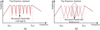
The reader in a frequency-domain-based RFID system normally interrogates the tag with an ultra-wide band (UWB) signal. The interrogation signal is reflected back to the reader, while specific resonances based on the tag structure, known as tag's frequency signature, are manipulated in the frequency domain of the backscattered signal. The reader then extracts the encoded data based on the detected resonances [Reference Preradovic, Balbin, Karmakar and Swiegers23–Reference Preradovic, Balbin, Karmakar and Swiegers25]. Depending on the bandwidth of the interrogation signal, various amounts of data encoding is feasible in the frequency domain-based systems. Normally, high data encoding capacity are suggested in the simulation process for a relatively small tag size (Fig. 1(a)). This content capacity is also achievable to some extent under laboratory condition based on the high-quality materials and precise fabrication process. However, there is major performance drop at the commercial phase of the frequency-based systems. Due to the printing errors and low-grade laminates such as paper and plastic, the commercial tags significantly suffer from resonators’ Q factor degradation, hence much lower data capacity is achievable; Fig. 1(b). Our research in commercial printing trials [Reference Azim, Karmakar, Roy, Yerramilli and Swiegers26] shows noticeable Q factor reduction of the resonators. Thus, significant shrinkage (at least five times) in the data-encoding capacity of the printed tag occurs. Moreover, the printing inaccuracy causes shifting in resonance frequencies, which again affects the content capacity and reliability of the printed tag to a level that is far below the expected data capacity [Reference Aminul Islam and Karmakar10, Reference Amin, Bhuiyan, Karmakar and Winther-Jensen27]. Therefore, one may conclude that the frequency domain-based systems fail to provide a reliable tag solution based on the commercial tag printing trials due to the immature cheap printing technology and low-grade laminates.
Tag frequency signature with (a) precise fabrication process and high-grade materials, (b) printed tag on paper substrate with conductive ink.

Therefore, it can be concluded that the conventional techniques in the chipless RFID systems are still to address the main requirements of the identification industries mainly on providing a fully printable tag solution on low-grade laminates with enough content capacity in a reasonable tag size.
III. EM-IMAGING FOR DATA DECODING
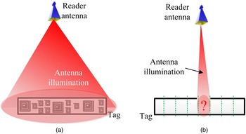
In all of the proposed techniques to date, the tag surface is thoroughly illuminated by the reader and the tag's data are retrieved simultaneously. Conversely, in EM-imaging every small section of the tag surface is scanned separately by the reader, while the tag's data are encoded in each section of the tag surface independently. Hence, the spatial diversity is also utilized in the EM-imaging approach [Reference Soumekh28, Reference Zomorrodi, Karmakar and Bansal29]. The spatial diversity of EM-imaging is compared with other conventional approaches in Fig. 2. There are two main questions regarding the proposed approach of EM-imaging, which shall be addressed: (i) how to precisely scan the tag surface; and (ii) how to encode data in a small section of the tag. These two questions are considered in this section.
Reading scenario in (a) conventional RFID systems, (b) image-based system.

A) Precise tag scanning
The required accuracy of the tag scanning directly relates to the expected data-encoding capacity. Many research entities assume 50-bits data-encoding capacity for a chipless tag structure as the ultimate capacity of these systems [Reference Preradovic, Balbin, Karmakar and Swiegers25, Reference Singh, Tedjini, Perret and Vena30, Reference Blischack and Manteghi31]. Moreover, for many RFID applications, the size of a credit card (85 × 54 mm2) appears to be the maximum allowable size of the RFID tag [Reference Preradovic and Karmakar8, Reference Aminul Islam and Karmakar10]. This may suggest one bit/cm2 as the very satisfying data-encoding capacity of a chipless RFID system.
 $$\hbox{Encoding capacity} = \displaystyle{{50} \over {8.5 \times 5.4}} = 1.089 \approx 1\,\,{\rm bit}\,/\,{\rm cm}^2.$$
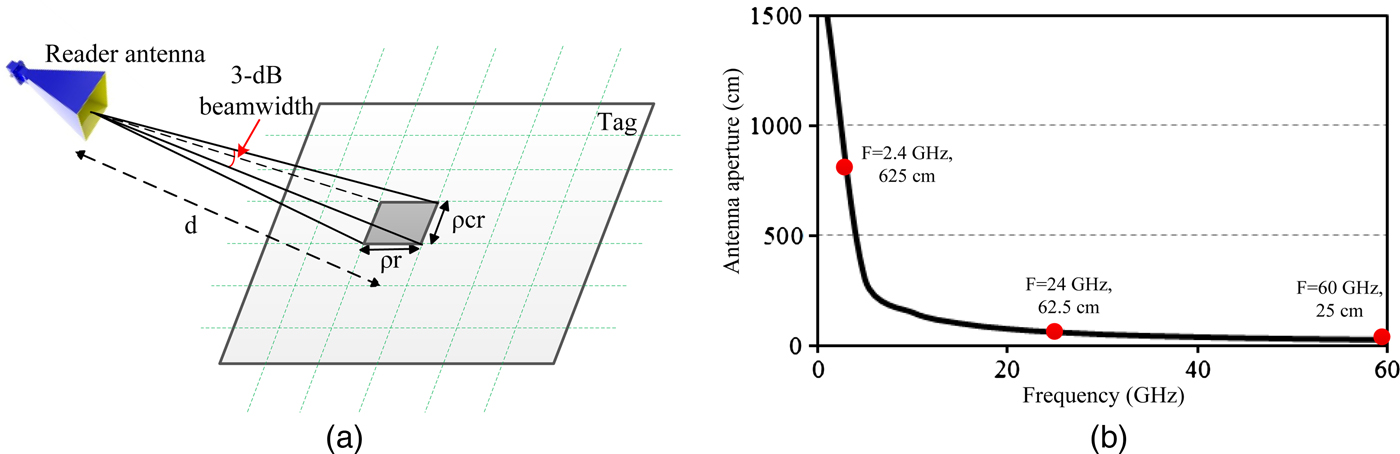
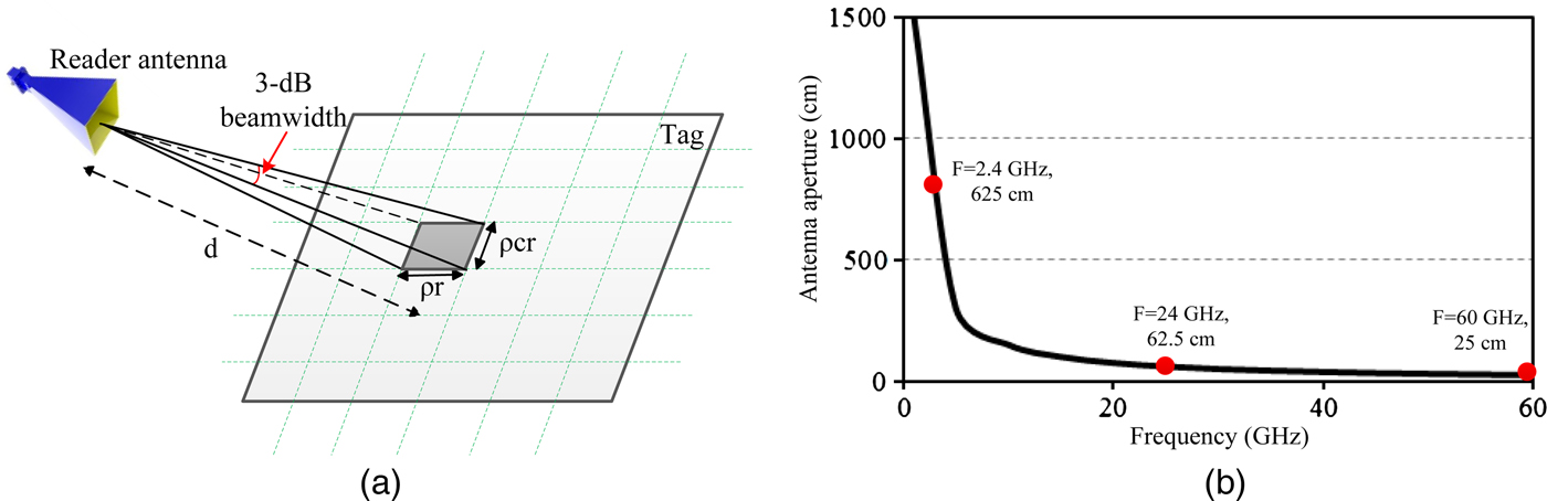
Therefore, the minimum scanning precession which is known as the reader footprint should be around 1 cm in the proposed image-based system. The reader footprint relates to the reader antenna 3-dB beamwidth and the reading distance as shown in Fig. 3(a). On the other hand, the antenna beamwidth depends on its aperture size. The required aperture size for 1° beamwidth at different industrial, scientific and medical (ISM) frequency bands is shown in Fig. 3(b). As one may notice, the required aperture sizes on lower frequencies are much larger than the normal reading range of chipless RFID systems, 50 cm. Therefore, antennas at lower ISM bands are not suitable on providing such a narrow required beamwidth. This is the main reason for selecting the mm-band 60 GHz for the proposed EM-imaging technique.
(a) Reader footprint on the tag surface. (b) Required aperture size for 1° beamwidth.
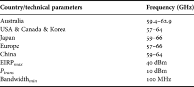
The band 57–64 GHz has been allocated globally to the fixed and mobile services by the International Telecommunication Union (ITU) [32]. Considering the high attenuation of this frequency band due to the oxygen absorption (15–20 dB/km) [33], the band is only suitable for low-range high-density radio communication applications. Table 1 shows the regulatory situation of this band along with some of its main technical requirements. Generous technical flexibilities, 40 dBm EIRP for example, compared with other ISM bands are given to 60 GHz band be regulators [34–Reference Guo, Qiu, Mo and Takahashi37].
Available Spectrum on 60 GHz band.

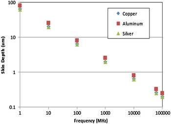
Moreover to the above-mentioned technical and operational advantages of the mm-band 60 GHz, there is an extra benefit of using this band in terms of tag cost reduction. It is well known that optimal tag reflection corresponds to metallic tags that are at least as thick as the skin depth. The skin depth as a function of radio frequency and material conductivity is shown in Fig. 4. Therefore, near-field communication (NFC) tags at 13.56 MHz; typically use >20 µm stamped aluminum, whereas UHF antennas (960 MHz) need only 5–10 µm stamped aluminum or plated copper. In the aforementioned frequency bands, the tag cost mainly controlled by the chip cost and components installation expenses and the amount of stamped aluminum is a small portion of the final tag cost. However, in a fully printable chipless RFID tags, the main cost depends on the tag size and the amount of required stamped aluminum.
Frequency versus skin depth in microns [Reference Buchar, Karmakar and Zomorrodi38].

The required thickness of aluminum or copper reduces to below 1 µm on mm-wave band 60 GHz. This results in significant cost reduction in printing process for the proposed technique [Reference Buchar, Karmakar and Zomorrodi38]. Therefore, the tag cost expectation of below 1¢ is completely feasible at 60 GHz band.
B) EM-polarizers as the data encoding unit
To independently encode data in each section of the tag in the proposed technique, it is required to form the tag's surface for creation of a unique EM-image. As a commercially printable tag structure is intended, only basic structures on the tag surface are suitable otherwise the system performance is affected by printing errors. Many objects were investigated by authors for such purpose. It was found that a straight strip line acts effectively as an EM-polarizer, hence the idea of cross-polar image-based system was initiated and developed [Reference Zomorrodi and Karmakar17, Reference Zomorrodi and Karmakar39]. The proposed cross-polar working basis provides significant system robustness toward multipath and clutter interferences [Reference Zomorrodi and Karmakar16], while these parameters known as major limiting factors in many conventional chipless RFID systems. The cross-polar working basis also provides the possibility of reading polarizer-based tag, while the tag is hidden in items. Hence, the secure identification is feasible in the proposed technique. Although straight strip line EM-polarizer shows good performance for data encoding purpose in the chipless RFID tags, a meander line-based tag found to be the more effective polarizer [Reference Zomorrodi and Karmakar16, Reference Zomorrodi and Karmakar40].
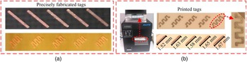
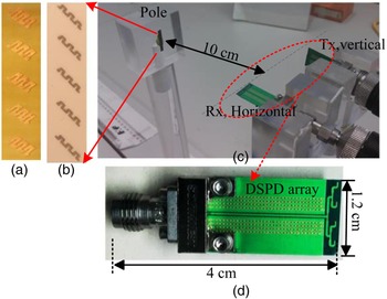
To verify the proposed concept, meander line and strip line-based tags are fabricated through different process technologies. First, tags are fabricated through a precise and costly printed circuit board (PCB) process by utilizing copper on a high-quality substrate, Taconic TLX-8 for example. Then the same tag is printed by a SATO printer utilizing the conductive ink over a paper substrate. These two types of tags are shown in Fig. 5. To test the performance of each tag, they are illuminated by a vertically polarized signal transmitted through a double-side printed dipole arrays (DSPDA) [Reference Zomorrodi and Karmakar41]. The tag is at 10 cm distance from the reader antenna. The backscattered signal is collected by the second set of DSPDA while the Rx antenna is oriented horizontally, hence the cross-polar working basis is maintained. Considering the size of DSPDA antennas, 12 mm, and the frequency of operation, the 10 cm reading distance ensures that the tag is in the far field of the reader antennas. Hence, the whole system may be classified as the far-field system.
Two tag types. (a) Precisely fabricated tags through PCB process and with high-quality materials. (b) SATO printed tags with highlighted anomalies.

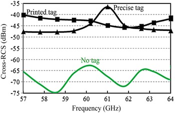
The measurement setup is shown in Fig. 6 with highlighted DSPDA. This antenna provides a suitable axial ratio that is crucial for cross-polar working basis [Reference Zomorrodi and Karmakar41]. Fig. 7 shows the measurement results. When no tag is in front of antennas, the signal level is below −65 dBm which represents the coupling between two antennas and the effect of plastic reading pole; Fig. 6(c). Having a precise tag creates significant cross-polar component with a peak at 61.3 GHz. This sharp cross-polar resonance behavior suggests the similar approach for data encoding as discussed in Section II for frequency-domain-based systems. However, if the precise tag is replaced by the printed tag, resonance is no longer existed on the response due to the low-grade laminates and limited ink conductivity. Printing errors and occurred shapes’ anomalies also matters in disappearance of the resonances as shown in Fig. 5(b). Regardless of vanishing resonances, the printed tag is interestingly still able to create noticeable cross-polar component in the backscattered signal. This measurement result builds the data-encoding scheme of the proposed image-based system.
(a) Precise meander line based tag. (b) Printed meander line based tag. (c) Measurement setup. (d) Reader DSPDA antennas [Reference Zomorrodi and Karmakar16].

Measured cross-polar component of precise and printed tags [Reference Zomorrodi and Karmakar16].

IV. ON/OFF DATA-ENCODING ALGORITHM
Based on the performance of the printed tag, it is clear that any resonance-based data-encoding technique fails to provide a practical encoding solution. Instead, one alternative is to detect the presence and absence of the EM-polarizers on the tag surface as the means of data encoding. In this approach, the tag surface comprises a certain number of pixels depending on the reader scanning resolution. When the reader scans a particular pixel, the presence or absence of the polarizer(s) results in a completely different received signal level at the cross-polar direction that acts as a binary data; existence of the polarizer(s) as “1” and no polarizer as “0”, for example. Therefore, a binary digit data encoding approach is implemented by the polarizers. No resonance is required to be detected from the backscattered signal for data encoding; hence, the proposed system would be robust to printing inaccuracy and low-grade materials.
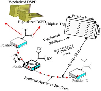
Creation of a precise scanning on the tag surface in millimeter order in the real scenario is a matter of question though. Based on the system parameters discussed earlier, the SAR theory shall be utilized on the reader side for achieving the fine scanning precision [Reference Soumekh28, Reference Sebastian, Robert, Ming-Shih and Martin42, 43]. In this approach, the reader equipped with small antenna(s) moves around the tag and illuminates the tag surface through different view angles; see Fig. 8. All the received signals are stored along with the information about the different reader positions. Then the SAR-based signal processing of the stored signals results in an image with very fine resolution which normally requires a much larger antenna aperture than that of the actual antenna(s) utilized in this technique.
SAR reading scenario for chipless tag [Reference Zomorrodi and Karmakar16, Reference Zomorrodi and Karmakar17].

Two image resolutions are normally related to the captured image; range and azimuth resolution. Range resolution shows the ability of the system to distinguish two objects at different ranges. The range resolution relies on the characteristics of the transmit signal. For a pulse-shaped transmit signal, the pulse width defines the range resolution by:
 $${\rho _r} = c\displaystyle{{{T_p}} \over 2} = \displaystyle{C \over {2B}},$$
where ρ r is the range resolution, c is the light speed, T p is the pulse width, and B is the equivalent pulse bandwidth. A fine range resolution is achievable by narrow pulses; however, a minimum pulse width is needed to satisfy the required average transmit power for the adequate signal-to-noise ratio. To satisfy these two contradictory requirements, a chirp pulse-shaped signal is normally used to provide enough range resolution with a reasonable average transmit power.
The ability to separate two targets along the track of the system is known as azimuth resolution. In the SAR technique, the azimuth resolution depends on the synthetic aperture size [Reference Soumekh28]:
 $${\rho _a} = 0.89\displaystyle{\lambda \over D},$$
where ρ a is the azimuth resolution, D is the size of the synthetic aperture, and λ is the wavelength.
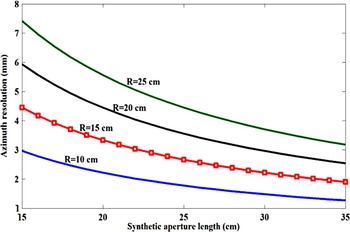
As discussed in Section III(a), the expected resolution on the tag surface shall be less than 10 mm to provide a competitive data-encoding capacity. Based on (2), providing such a small resolution in range direction requires large bandwidth, in GHz order, that would be difficult or expensive to have. On the other hand, the azimuth resolution is independent of the bandwidth and only relies on the synthetic aperture size. Fig. 9 represents the required aperture size for the normal reading range of the chipless RFID systems at 60 GHz band. As is clear from the graphs, the required aperture size in the SAR technique is quiet practical for azimuth resolution of millimeter order in the 60 GHz band. For example, less than 6 mm azimuth resolution is achievable with only 20 cm of the synthetic aperture size at 25 cm reading distance. Therefore, it could be concluded that fine range resolution is unlikely to be achieved with the limited bandwidth. The final data-encoding capacity of the proposed system shall rely on azimuth resolution only. This simply means that the tag surface in Fig. 8 can be divided into multiple vertical slices. Each slice is detectable separately through fine azimuth resolution, while reader is not able to detect the number of polarizers on each column (slice). Providing enough signal strength on the reader side, five EM-polarizers are assumed at this article on each slice of the tag surface. When the moving reader finishes a full synthetic aperture scanning, the effect of each vertical slice of the tag is separately analyzed after signal processing. Based on the presence or absence of the polarizers, the reader then receives significantly different cross-polar radar cross-section (cross-RCS) levels that can be used in the decoding algorithm.
Azimuth resolution versus synthetic aperture.

As discussed earlier, the SAR-based signal processing requires relative movement of the reader and tag. For the case when tags are moving over a conveyer belt with constant speed, it is possible to have a fixed reader. However, this is a very unique scenario and for general applications which tags are fixed, a moving reader is mandatory to maintain the relative movement of the reader and tags. This general scenario is shown in Fig. 8. The reader moves around the tag and stops at different view angles for reading and capturing the tag response. The sampling points are 2 mm apart from each other. By considering the required aperture size of 20–30 cm, noticeable number of transmit and receive, 100–150 times, are required. The requirement for physical movement of the reader and frequent stopping seems to be a big drawback of the proposed image-based system as it results in very slow reading time. One solution is to capture the tag's backscattered signals, while reader continuously moves around the tag, similar to earth imaging by space platforms [Reference Soumekh28]. In this scenario, a Doppler frequency shift due to continuous movement of the reader is expected and shall be considered in the signal processing. It is important to note that movement of the reader is not based on the operator's hand movement. Obviously, the speed, aperture length and other factors cannot be maintained accurately through manual movement. Instead, the reader moves over a rail while controlled by a motor. This approach provides much faster reading process time than the “stop and move” scenario in order of 300–500 ms, but still is not considered very competitive. However, after proofing the concept of the theory through reader physical movement, other alternative approaches is possible for much faster reading process with reasonable hardware complexity [Reference Zomorrodi and Karmakar44].
V. SALIENT ATTRIBUTES OF THE EM-POLARIZER-BASED TAG
The proposed EM-imaging technique at mm-band is different than other conventional approaches reported so far in many features. Three main aspects which can be highlighted are:
-
– Image-based instead of working on time or frequency domain: It was already discussed that data encoding based on the tag's EM-image provides system robustness towards fabrication tolerance and also low-grade materials. While other conventional techniques are severely suffering from printing errors and experiencing noticeable performance degradation due to the commercial printing laminates [Reference Amin, Bhuiyan, Karmakar and Winther-Jensen27], paper and conductive ink, the proposed image-based system shows its ultimate performance based on a real printed tag structure without any data-encoding capacity shrinkage.
-
– Cross-polar working basis rather co-polar: The majority of suggested techniques in the chipless RFID systems are co-polar basis, while the proposed technique is cross-polar-based system. The cross-polar working basis provides huge practical advantages. As analytically shown by Vena et al. through an equivalent circuit model, the cross-polar systems are very robust toward multipath interferences [Reference Vena, Perret and Tedjni45]. This aspect of the system was verified through measurement in this work as well. While a printed meander line-based tag was read through the reader antennas, multiple reflective objects, horn antennas, and circuit boards, were placed closely in the reading zone. The measurement showed that the tag's cross-polar backscattered signal is highly immune to the multipath signals created by the surrounding objects. The detailed description of the measurement set up and the results were published by authors [Reference Zomorrodi and Karmakar16]. To stimulate the clutter situation, a large metal plate was located in front of reader. However, the measurement result confirmed that the tag-reading process is not affected at all [Reference Zomorrodi and Karmakar16]. Considering the system performance toward severe multipath and clutter interferences, the suggested technique would be very suitable for industrial environments.
-
– Much higher frequency band of operation: The proposed frequency band of operation for the imaging technique is much higher than that of already suggested and utilized for other conventional chipless RFID systems. This may raise concern about the adverse effect of mm-band of 60 GHz considering its high oxygen absorption [33] and significant path loss based on Friis equation [Reference Balanis46]. Therefore, the initial expectation is that the system is very vulnerable to blockage and so the application would be only limited to the optical LoS similar to barcodes. This issue is considered and the system sensitivity to blockage is investigated in this communication which reveals another interesting aspect of the proposed system. Moreover, very small wavelength of operation suggests the miniaturized tag size. In addition to the small tag size which suggests higher data encoding capacity, the system robustness toward tag bending would be also interesting. These two aspects of the proposed system are discussed in this section.
A) EM-LoS versus optical LoS
The “line-of-sight” terminology in EM theory refers to propagation of EM-waves including optics in a straight line. Based on the frequency of operation, a radiocommunication link may be referred to as LoS or NLoS. LF EM-wave does not need a LoS condition, HF broadcasting for examples. For higher bands, the transmitter shall see the receiver to be able to communicate effectively or a LoS condition is required, point-to-point communication in GHz bands for example. Based on this assumption, the proposed technique is definitely a LoS system. Therefore, the reader requires LoS condition to detect and read the tag.
However, the LoS systems may be categorized further. The communication link in some LoS systems may require a clear/visible LoS between Tx and Rx without any obstacles. Very HF EM-wave and specifically optical communication systems are in this category. These systems are referred to as optical LoS systems in this article. However, there are LoS systems that operate effectively even if some obstructions, in the form of EM-wave transparent materials, are in the reading zone. These types of systems are referred to as EM-LoS in this communications. The optical based identification systems, barcodes and QR codes, are definitely optical LoS systems. Any barrier, even dirt may results in reading failure. This restricts the system flexibility and is seen as one of main issues of barcodes for many applications.
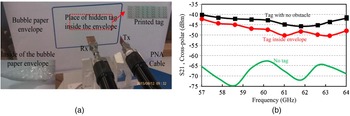
Considering the mm-wave band of operation, it is important to evaluate the system performance when the tag is read in EM-LoS only with some barriers between the reader and tag, tag in an envelope for example. For this purpose, the printed tag is placed inside a bubble paper envelope as shown in Fig. 10(a). The reader antennas are DSPDAs oriented orthogonally, similar to Fig. 6, and connected to the Performance Network Analyzer (PNA) Agilent E8361A. The S 21 in dB versus frequency shows the cross-RCS of the covered tag by the envelope. This result is compared with the case when the tag is in front of antennas without any obstacle.
(a) Secured tag in a bubble paper envelope. (b) Measurement results.

The measured results and the images of the measurement setup are shown in Fig. 10. As is clear from graphs of Fig. 10(b), the system is adequately capable of detecting the presence or absence of the tag, based on different measured cross-RCS levels. The reduction in the signal level when the tag is hided inside the envelope is minor and still is well above the signal level when no tag is read. This is a significant aspect of the system because it provides a None-optical LoS secured identification of objects inside an envelope without opening them. The mm-wave signal is very lossy and mainly requires an optical LoS reading condition. However, as the system is cross-polar basis, the receiver is capable of detecting even a weak signal due to the natural cancelation of background noise. This provides a substantial advantage for the reading process. This simply means that in practical scenarios, the tagged objects can be packaged without affecting the data-decoding process. It is important to emphasize that the results in Fig. 10 are without any calibration process. Obviously, if the environmental effects are cancelled out with a predefined calibration process, then much cleaner signal level differences between the two cases is observed. This process may ease reading of the tag when it is hided inside much more thicker items than bubble paper.
B) Bending effect
In real identification and tracking applications, the tags are vulnerable to bending based on the shape of the item which tags are attached. This issue may affect the tag's encoding capacity. There are very limited published works on the study of identification system degradation, RFID or Barcodes, due to the bending effect [Reference Siden, Jonsson, Olsson and Wang47]. It is important to explore how the tag bending may affect the reading process in the proposed image-based technique.
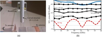
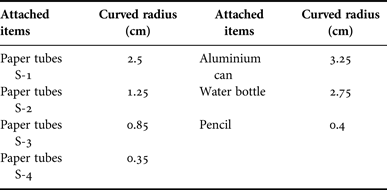
To verify the performance of the proposed EM-polarizer-based tag with respect to bending, small paper rolls of varying radii are prepared to which the tag can be attached. The radii of the rolled papers along with the radii of some commonly used objects are summarized in Table 2. Figure 11(a) shows the measurement setup that is similar to previously shown in Figs 6 and 10. Two separate antennas are utilized as Tx and Rx at 10 cm distance to the reading pole. Antennas are connected to the PNA and the measured cross-RCS is shown in Fig. 11(b). It is clear from the results that for objects bigger than S-1(R = 2.5 cm), bending has negligible effect on the received power level. Examples include a water bottle and aluminum can. This clearly confirms system robustness for a wide variety of objects. In other words, any object bigger than a water bottle experiences no bending effect in the proposed technique. For objects with radii smaller than 2.5 cm, the received power level gradually decreases. However, the receiver still would be able to separate the signal of a bent tag from the “no tag” case. Only for items smaller than S-4 (0.35 cm radius), like a pencil, bending significantly degrades the system performance. Therefore, the proposed system provides a fairly high robustness toward bending due to its miniaturized tag size and image-based working basis.
(a) System structure for measuring the bending effect. (b) Measurement results.

Radii of the paper tubes and some well-known items.

VI. SIGNAL PROCESSING AND FINAL RESULT
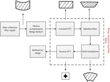
The Range Migration Algorithm (RMA) as proposed in [Reference Carrara, Goodman and Majewski48] is followed for the SAR-based coding. The captured data based on various positions of the reader antenna, known as the raw signal, is processed by the RMA SAR-based algorithm. The RMA normally is divided into the following steps:
-
– Data collection,
-
– Azimuth Fourier transform,
-
– Matched filter,
-
– Stolt interpolation,
-
– Inverse Fourier transform, and
-
– Reflectivity image
when the reader moves around the tag, in each specific position, a two-dimensional (2D) data matrix is produced which contains the range profile data. Hence, the collected data have the formation:
 $$S\;\left( {{x_i},w(t)} \right),$$
where x i contains the information of the reader position and the w(t) is the instantaneous of the chirp signal and defines by (5), while the c r is the chirp rate, f c is the center frequency of the signal, and BW is the signal bandwidth:
 $$w(t) = \,2\pi \left( {{c_r}t + {f_c} - \displaystyle{{BW} \over 2}} \right).$$
The matrix format of (4) is considered as the raw signal by the codes for SAR-based signal processing. In the RMA approach, the azimuth Fourier transformation is applied to this raw signal. This is the main difference between the RMA and other conventional approached in SAR-based signal processing, polar formation algorithm for example. The Fourier transformation changes the time-domain signal, S(x i , w(t)), to its equivalent wave number domain, S(k x , kr ).
The next phase of the RMA is the application of a 2D phase compensation to the azimuth-transformed signal [Reference Carrara, Goodman and Majewski48]. This operation perfectly modifies the range curvature of all scatterers at the same range as scene center. The matched filter is defined through the following expression on which the R s shows the distance between to the target center [Reference Carrara, Goodman and Majewski48, Reference Charvat49]:
 $${S_{mf}}({k_x},{k_r}) = {e^{j{R_s}}}\sqrt {k_r^2 - k_x^2}. $$
Following the matched filter step, Stolt interpolation is applied in the RMA algorithm. It simultaneously compensates the range curvature of all scatterers by an appropriate warping of the SAR signal data. This means that the 2D SAR data from the wave number domain (k r ) to the spatial wave number domain k y through the following expression [Reference Carrara, Goodman and Majewski48]:
 $${k_y} = \sqrt {k_r^2 - k_x^2}. $$
A 1D interpolate must be conducted across all the azimuth wave number k r to map them onto k y thus resulting Stolt interpolated matrix S st (k x , ky ) [Reference Charvat49]. At this point in the RMA, the processed signals from all scatterers are 2D linear phase gratings. A 2D inverse Fourier transform is computed to fully compress the scatterers in range and azimuth [Reference Carrara, Goodman and Majewski48]. The above-mentioned process can be summarized as shown in Fig. 12.
Image formation processing using RMA [Reference Carrara, Goodman and Majewski48].

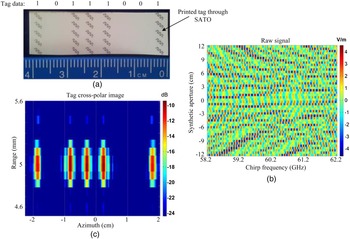
The above concept and the signal processing steps are applied to an 8-bits printed tag. The aperture size which reader moves around the tag is 24 cm. The reading distance is 10 cm similar to previous steps in this communication. The tag structure, the captured raw signal based on the frequency and the reader position, and finally the cross-polar EM-image of the tag are shown in Fig. 13. As one may notice, the tag's image successfully decodes the tag content by effectively finding the column of EM-polarizers on the tag surface. The received signal level from the five polarizers is 14 dB higher than that of the rest of reading scene which provides a reliable reading process.
(a) A 8-bit printed tag with 4 cm length. (b) Raw signal based on the 24 cm aperture size at 10 cm reading distance. (c) Tag's cross-polar image shows the position of the meander lines as decoding algorithm.

It is essential to mention that the azimuth resolution shown in Fig. 13 is the actual and real azimuth resolution achieved after signal processing. However, the range resolution in Fig. 13 is not real and is selected for display purpose only. In fact, the actual range resolution is much courser than that of shown in Fig. 13.
The final achieved azimuth resolution is 5 mm as shown in Fig. 13. The width of tag is around 10 mm as it includes five polarizers on each column. Therefore, the detectable data-encoding capacity of the printed tag is 2 bits/cm2. For a tag of 8.5 × 1 cm2, 17 bits can be encoded. This tag is 5.5 times smaller than a credit card (8.5 × 5.5 cm2).
VII. CONCLUSION
An image-based, chipless RFID tag has been proposed. The tag is fully printable hence is low cost and capable of providing high data-encoding capacity in a small tag size. The tag requires minimum amount of conductive ink to perform properly. The printing inaccuracy has been considered in the proposed approach. The system is immune to clutters and multipath interferences, and therefore, is very suitable for industrial applications. It also shows high robustness toward tag bending effect. Another interesting aspect of the proposed technique is the ability of reading tag while it is hidden in a paper envelope. Therefore, secure reading is possible in this approach. The reader utilizes two separate orthogonally oriented printed antennas on 60 GHz band. At this stage, the physical movement of the reader is required to provide a synthetic aperture that is needed for signal processing. All measurements were done with low-cost inkjet-printed tags in normal laboratory environment without any pre-calibration or background cancellation process. The measurement results have proven the validity of the proposed concept.
ACKNOWLEDGEMENTS
The project is supported by Australian Research Council's Discovery Project Grant DP110105606. Moreover, Xerox, USA, supports the work through University Affairs Committee (UAC) Grant, mm-wave Chipless RFID tag, File/HE 1721-2015.
 Dr. Mohammad Zomorrodi received the BSc and MSc degree in electrical engineering (major in communication) from Iran in 1995 and 2000, respectively. He has worked for more than 10 years in telecommunication regulatory and ITU related issues. He graduated with PhD in Electrical engineering from Monash University, Melbourne, Australia in 2015. His research interest is antenna and microwave design, radar technology and RFID systems.
 Dr. Nemai Chandra Karmakar graduated with BSc (EEE) and MSc (EEE) from Bangladesh University of Engineering and Technology in 1987 and 1989, respectively, MSc in EE from the University of Saskatchewan, Canada in 1992, PhD in ITEE from the University of Queensland in 1999, PGDipTHE from Nanyang Technological University in 2001 and MHEd from Griffith University in 2007. He worked as a microwave design engineer at Mitec Ltd., Brisbane from 1992-1995 and contributed significantly to the development of Australian Optus Mobilesat smart antennas. He taught senior level courses in electronics, radar, microwave active and passive design and antennas at QUT, NTU, and Monash University. He has been working with many industry partners on various collaborative research projects on fully printable chipless RFID tags and sensors for ubiquitous tagging and sensing, wireless power transmission, microwave biomedical imaging and devices, smart antennas for mobile satellite communications and diagnostics of faulty power equipment. He has nine patent applications in chipless RFID and sensors, edited and authored eight books and about three hundred refereed journal, conference and workshop publications. A/P Karmakar is a graduate member of IEAust and a senior member of IEEE.