I. INTRODUCTION
Solution processable reduced graphene oxide (RGO) is of great interest due to their tunable electronic and optoelectronic properties as well as their potential in energy applications.Reference Singh, Joung, Zhai, Das, Khondaker and Seal1–Reference Joung and Khondaker14 In addition, RGO can be synthesized in large quantities at low cost.Reference Singh, Joung, Zhai, Das, Khondaker and Seal1–Reference Bonaccorso, Colombo, Yu, Stoller, Tozzini, Ferrari, Ruoff and Pellegrini3,Reference Tung, Allen, Yang and Kaner6,Reference Compton and Nguyen7 Their easy solution processability makes them ideal candidates for large area device applications. Moreover, due to the presence of defects and oxygen functional groups in RGO, it can be an ideal template for the decoration of different types of organic and inorganic nanomaterials which allow one to obtain a new class of multifunctional materials,Reference Singh, Joung, Zhai, Das, Khondaker and Seal1,Reference Wan, Huang and Chen2,Reference Cao, Zhu, Xu and He15–Reference Das, Chakraborty, Chakrabarty, Ghosh and Pal27 resulting further tunability of device properties.Reference Cao, Liu, Chu, Wu, Ye, Cai, Chang, Wang, Gong and Liu20,Reference Chang and Wu21 An interesting device prospect for RGO is its potential application in the field of photodetectors (PDs) and phototransistors (PTs).Reference Ghosh, Sarker, Chunder, Zhai and Khondaker11 High-performance PDs and PTs are key components for the realization of imaging, sensing, and communication devices.Reference Ando and Kimachi28,Reference Goossens, Navickaite, Monasterio, Gupta, Piqueras, Pérez, Burwell, Nikitskiy, Lasanta, Galán, Puma, Centeno, Pesquera, Zurutuza, Konstantatos and Koppens29 A PT is preferable over a PD as it offers additional tuning of photoresponsive gain by tuning the gate voltage.Reference Pal, Arif and Khondaker30
The majority of the PTs that are used in practical applications are made of inorganic materials such as single-crystal silicon,Reference Johnson and Chiang31 amorphous silicon,Reference Kaneko, Koike, Tsutsui and Tsukada32 and InAlAs–InGaAs due to their high level of current gain of few hundred in homojunctions to few thousands in heterojunctions.Reference Choi, Kang, Choi, Kim, Choi, Kim, Jang and Seo33 Solution-processed PTs are advantageous, due to their ease of materials processing, mechanical flexibility, light weight, ability of tuning properties by molecular design, and large-area coverage at low fabrication cost via spin coating, drop casting, and inkjet printing.Reference Forrest34–Reference Facchetti, Yoon and Marks36 RGO-based PTs are desirable as they can be easily printed or coated on virtually any substrate in ambient condition for flexible, wearable electronics at relatively low cost. They may complement the currently prevalent silicon technology in particular in flexible devices. In addition, the ability to tune the semiconducting property (such as carrier type) of the host material via light could be of great significance for the realization of optically induced electronics where it is envisioned that the logic operation will be performed by selective exposure of the device to light.Reference Fang, Wang, Liu, Schlather, Ajayan, Koppens, Nordlander and Halas37 An important consideration in designing and fabricating RGO-based PDs and PTs could be the utilization RGO’s potential as an acceptor material when mixed with suitable photoactive small molecules which could give rise to large donor/acceptor (D/A) interfaces for charge generation and provide a continuous pathway for electron transfer.Reference Chang and Wu21 However, fabrication of RGO-based PTs using such an approach has received little attention.
In this paper, we report the fabrication and electronic transport investigation of RGO PTs where copper phthalocyanine (CuPc) has been used as a photoactive donor material. Phthalocyanine (Pc) molecules are optically active materials, which have been used in thin film transistors, light emitting diodes, and organic solar cells.Reference Wang, Zhang, Xing, Yuan, Yan and Han38–Reference Zhang, Gan, Cao, Wang, Qi and Guo45 In addition, Pc molecules are appreciably stable toward thermal and chemical treatment. Their metal salt solutions have a very good film-forming property with high purity, and their salt derivatives have been blended with carbon nanotube to produce Pc sensitized nanotube thin film with potential application in solar cell.Reference Hatton, Blanchard, Stolojan, Miller and Silva40 Therefore, Pc is of particular interest for incorporation into RGO as it is considered as an electron donor material.Reference Bao, Lovinger and Dodabalapur39 We synthesized a composite of RGO/tetrasulfonate salt of CuPc (TSCuPc) and fabricated PT devices with a channel length (L) and width (W) of ∼5 µm × 200 µm by dropcasting the composite on a bottom gate field effect transistor (FET) geometry. In the dark, the device showed a p-type FET behavior due to the trapping of electrons at the TSCuPc/RGO interface. At low light intensity, the device shows ambipolar behavior with a weak p-branch due to a light-induced quenching of holes resulting in negative photocurrent I ph and a strong n-branch due to a light-induced electron transfer from TSCuPc to RGO. With increasing light intensity, only an n-type behavior was observed with a gradual increase of electron current. The demonstration of high-performance RGO-based visible light sensitive PTs with the ability of tuning carrier type paves the way to integrate these devices in various optoelectronic circuits for optical communications, remote sensors, and optical detectors.
II. EXPERIMENTAL DETAILS
A. Synthesis of RGO/TSCuPc
RGO sheets containing TSCuPc molecules are synthesized through the reduction of graphene oxide (GO) (synthesized via Hummer’s method) in the presence of water-soluble semiconducting TSCuPc molecules following our previously published technique.Reference Chunder, Pal, Khondaker and Zhai24 In brief, 10 mg of GO powder was dispersed in 10 mL of deionized (DI) water and sonicated using a cup-horn sonicator for 30 min to create a homogeneous solution. A 10 mL of resulting GO dispersion was then mixed with 25 mL of 0.01 M TSCuPc aqueous solution in a round-bottom flask with a magnetic stir bar. Hydrazine hydrate was added to the solution followed by heating the solution to 90 °C for 1 h under constant stirring. The color of the solution changed from dark blue to dark green suggesting the successful attachment of TSCuPc on RGO. A dilute composite aqueous solution was spin-coated onto a freshly cleaved mica substrate and left overnight for drying. The structural characterizations of the RGO/TSCuPc composites were obtained by using atomic force microscopy (AFM), X-ray diffraction (XRD), and Raman spectroscopy. AFM imaging was carried out by using a Dimension 3100 (Veeco Instruments Inc., Woodbury, New York). A Rigaku-Miniflex II powder diffractometer (Rigaku, Tokyo, Japan) with Cu Kα (λ = 1.5418 Å) radiation operated at 30 kV and 10 mA was used to characterize XRD. Raman spectra were recorded from powder samples of RGO, TSCuPc, and RGO/TSCuPc at room temperature using a Renishaw Invia Raman microscope (Renishaw, Wotton-under-Edge, United Kingdom) equipped with a 514 nm excitation laser.
B. Device fabrication
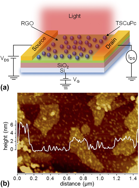
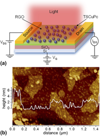
The RGO/TSCuPc films were integrated into a three-terminal bottom contact, bottom gate FET device. Figure 1(a) illustrates a cartoon of our device structure with the optoelectronic transport measurement setup. Source and drain electrodes of 5 µm channel length and 200 µm width was defined using standard photolithography on a highly doped silicon (Si) substrate capped with a thermally grown 250 nm SiO2. This was followed by thermal evaporation of 3 nm chromium (Cr) and 45 nm gold (Au) and a standard lift-off. Prior to the deposition of the RGO/TSCuPc composite film, the wafer was cleaned in acetone and isopropyl alcohol (IPA), respectively, for 5 min each. RGO/TSCuPc was then dropcasted, and the solvent was allowed to evaporate in a fume hood for a few hours. Devices were then further annealed at 120 °C for an hour to remove any excess moisture. The average film thickness was ∼40 nm measured by AFM.
(a) Schematic of a RGO/TSCuPc phototransitor under light illumination and optoelectronic transport measurement setup. (b) AFM image of TSCuPC attached RGO sheets and the small dots on RGO sheets are TSCuPc.

C. Optoelectronic transport measurements
The electrical transport measurements in the dark and under illuminated conditions were carried out in a probe station placed inside a glove box with oxygen content <0.5 ppm. The data were taken using an Agilent 4145B semiconductor parameter analyzer (Agilent Technologies, Santa Clara, California) connected with a probe station. A xenon lamp (solar-light simulator, Oriel 96000, Newport Corporation, Irvine, California) was used as the white light illumination source. The spot size of the beam was ∼30 mm in diameter and covered the whole sample. The optical intensity was measured with a calibrated silicon photodiode.
III. RESULTS AND DISCUSSION
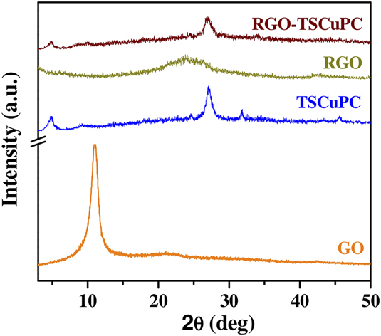
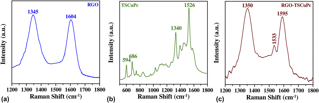
Figure 1(b) shows an AFM image of RGO sheets containing TSCuPc molecules which were spin-coated on a mica substrate. The small dots in the image are TSCuPc molecules that are well distributed on the RGO sheets. The AFM height analysis [white line in Fig. 1(b)] indicates that the heights of the TSCuPc/RGO sheets are ∼2 nm. Since the height of a single layer RGO sheet was found to be ∼1 nm,Reference Joung, Chunder, Zhai and Khondaker41 we estimated the height of the TSCuPc molecule to be ∼1 nm.Reference Chunder, Pal, Khondaker and Zhai24 The powder XRD technique of GO, TSCuPc, RGO, and RGO/TSCuPc composites was used to determine the structural composition of the materials, and the diffraction patterns are presented in Fig. 2. The XRD pattern of GO shows a sharp well-distinct peak centered at 10.5°, which corresponds to d-spacing of ∼0.84 nm. The larger d-spacing compared to natural graphite (∼0.335 nm) establishes the comprehensive oxidation of graphite to GO with the formation of hydroxyl, epoxy, and carboxyl groups.Reference Kim, Park, Woo, Kim, Kim and Yun46 In the diffraction pattern of RGO/TSCuPc, the signature peak of GO stacking is fully disappeared, and all the peaks of TSCuPc are clearly observed, demonstrating the successful integration of TSCuPc into RGO. Moreover, no diffraction peaks for RGO can be found in the RGO/TSCuPc composites, might be due to the low quantity and comparatively low diffraction intensity of RGO in the composite. The charge transfer interaction between TSCuPc and RGO was confirmed by Raman spectroscopy. Figs. 3(a)–3(c) show the Raman spectra of RGO, TSCuPc, and RGO/TSCuPc composites, respectively. The two characteristics bands at 1345 cm−1 (D band) and 1604 cm-1 (G band) of RGO are shown in Fig. 3(a). The most intense Raman bands for TSCuPc can be found at 1526, 1340, 686, and 594 cm−1. In Raman spectroscopy of the RGO/TSCuPc composite, the G band appeared at 1595 cm−1, which is downshifted by 9 cm−1 compared to that of RGO. On the other hand, the D band showed at 1350 cm−1, which is upshifted by 5 cm−1, an indication of the donor–acceptor composite system.Reference Su, Pang, Alijani, Li, Feng and Mu¨llen47 A decrement of the G band due to the augmented large quantity of charge offered by the aromatic TSCuPc molecules on the basal plane of the RGO sheet is observed, which ultimately increased the height of the Fermi level. A new peak was observed at 1533 cm−1 due to the peak overlapping between the donor (TSCuPc) and acceptor (RGO) in the composites and confirms the formation of the hybrid structure.
XRD patterns of GO, TSCuPc, RGO, and RGO/TSCuPc.

Raman spectra of (a) RGO, (b) TSCuPc film, and (c) RGO/TSCuPc composite film.

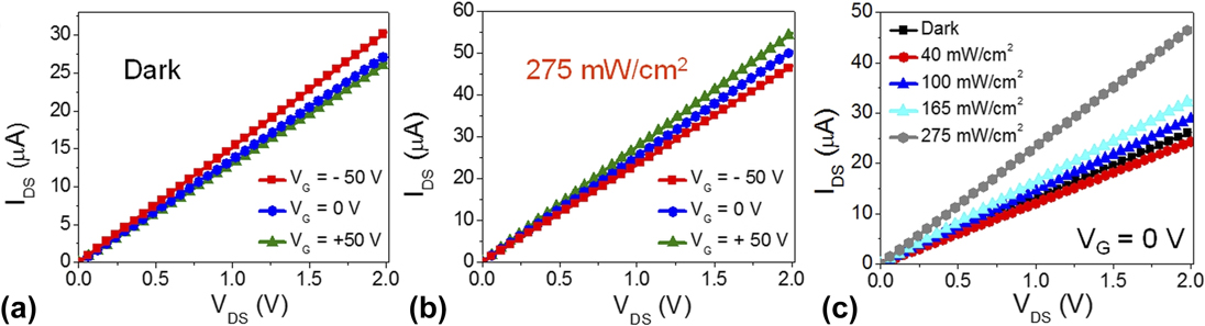
Figure 4(a) shows a plot of source-drain current (I DS) versus bias voltage (V DS) at different gate voltages (V G) (output characteristics) of a representative RGO/TSCuPc device measured in the dark. The V G values were +50, 0, and −50 V (bottom to top). We observed that the current increases with decreasing gate voltage, typical of a p-type FET behavior. Subsequently, we measured the output characteristics of the same device with a light illumination of 275 mW/cm2 intensity for the same gate voltages [Fig. 4(b)]. Unlike the measurement under dark, the current decreases with decreasing gate voltage, indicating that the device has converted to an n-type FET with light. To further investigate the photo-induced response, we measured the I DS − V DS characteristic of the same device measured under different illumination intensities of 0, 40, 100, 165, 235, and 275 mW/cm2 with V G = 0 V [Fig. 4(c)] (Due to the unavailability of neutral density filter in our solar simulator, we were unable to study photoresponse below 40 mW/cm2). We observed that as the intensity of the light increased, the current also increased. These results indicate that the current can be modulated by light intensity as well as by gate voltages, a hallmark of a PT.
Output characteristics (I DS − V DS) of a RGO/TSCuPc phototransistor for different V G of −50 (Red curve), 0 (Blue curve), and +50 V (Green curve) (a) in dark condition and (b) under illumination of 275 mW/cm2. (c) I DS − V DS of varying illuminated light power intensities with V G = 0 V. The light intensities were 0, 40, 100, 165, and 275 mW/cm2.

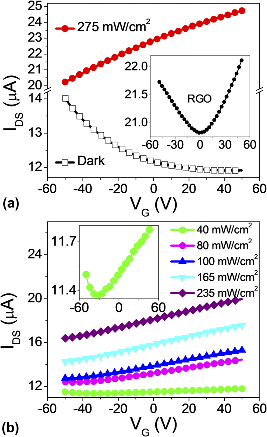
To more clearly show the effect of the gate voltage and light intensity on the performance of the RGO/TSCuPc PTs, I DS − V G characteristics were measured in the dark and at different light intensities. Figure 5(a) shows I DS plotted versus V G of the same RGO/TSCuPc device measured in the dark, where the V G was swept from −50 to +50 V with a constant V DS of 1 V. The device shows a p-type FET behavior with a hole mobility (μh) of ∼0.095 cm2/Vs calculated from µ = (L/WC oxV DS)(∆I/∆V G), where C ox is the capacitance per unit area of the gate insulator. This mobility value is lower than that of pure RGO sheets.Reference Joung, Chunder, Zhai and Khondaker41,Reference Joung, Chunder, Zhai and Khondaker43 This observation indicates that in the absence of the light, the TSCuPc is more insulating (or low mobility) than RGO.Reference Zhen, Shang, Liu, Tu, Ji, Liu, Liu, Liu and Wang44 Thus, TSCuPc molecules in RGO worked as a scattering center and hinder the path of flow of the charge carrier. Such a decrease in the mobility (or conductivity) in the composite also has been observed in PbS decorated grapheneReference Zhang, Gan, Cao, Wang, Qi and Guo45 and RGO/CdSe composites.Reference Geng, Niu, Xing, Song, Liu, Sun, Cheng, Zhong, Liu, Zhang, Sun, Xu, Lu and Liu26 The p-type FET behavior in RGO has been reported in ambient condition and explained by oxygen doping.Reference Joung, Chunder, Zhai and Khondaker41,Reference Ryu, Liu, Berciaud, Yu, Liu, Kim, Flynn and Brus48,Reference Chakraborty, Chakrabarty, Das, Ghosh and Pal49 Since we measured our device in an oxygen-free glovebox, oxygen doping is not expected. To confirm this, a control experiment was performed on a pure RGO device which showed ambipolar behavior in the glove box [the inset of Fig. 5(a)]. The RGO sheets were synthesized under identical condition except in the absence of TSCuPc. Hence, the p-type behavior of our RGO/TSCuPc device must be due to the interaction of the TSCuPc molecule with RGO. The possible reason for the p-doping is as follows: the positively charged Cu ion (cation) in TSCuPc molecules may interact with mobile electrons in RGO sheets in the darkness; hence the mobile electrons in RGO can be trapped at TSCuPc molecules/RGO interface, making it predominantly p-type FET.
(a) Transfer characteristics I DS − V G characteristics of a RGO/TSCuPc phototransistor in the dark and under light illumination of 275 mW/cm2. Inset: I DS − V G characteristics of RGO only device. (b) I DS − V G characteristics of the same RGO/TSCuPc device under light illumination of 40 (inset), 80, 100, 165, and 235 mW/cm2. V DS = 1 V.

Unlike the p-type property observed in the dark, with the light illumination of 275 mW/cm2, the device shows well-defined n-type behavior [Fig. 5(a)]. Another important observation is that there is a large increase in current at all voltages under light illumination. For example, the dark current in RGO/TSCuPc at V G = −50, 0, and +50 V is ∼14.0, 12.2, and 11.9 µA, respectively, while the current under illumination (275 mW/cm2) is ∼20.2, 22.9, and 24.7 µA. The current increases by ∼44, 88, and 110% for V G = −50, 0, and +50 V, respectively. This observation clearly demonstrates that light and gate voltages have a significant effect on the photoresponse of the RGO/TSCuPc composite. Therefore, our novel hybrid PTs can be advantageous as they offer flexibility in controlling the carrier type with solar light illumination combined with an increase in current (or electron mobility) of the PT.
To more systematically study the effect of light intensity on the photoresponse of RGO/TSCuPc, we measured the I DS − V G characteristics under light illumination with intensities of 40, 80, 100, 165, and 235 mW/cm2. This is shown in Fig. 5(b). At light illumination of 40 mW/cm2, the device shows ambipolar FET characteristics with enhanced current in electron branch compared to that in the hole branch [the inset of Fig. 5(b)]. A threshold voltage V th (or minimum conductance point) of ∼ −35 V is observed. The hole current (at V G = −50 V) is reduced from ∼14.05 to ∼12.45 µA, while the electron current at V G = +50 V is ∼11.8 µA, similar to the current value in the dark. As the intensity of the light further increased, the V th was not observed within the V G ranges of −50 V to +50 V, and the device showed only an n-type FET behavior. In addition, the current gradually increased at all gate voltages. Notably, we found a decrease in μh and an increase in μe as the light intensity increased. The μh was ∼0.095 and 0.022 cm2/Vs for 0 and 40 mW/cm2, and μe was ∼0.018, 0.034, 0.052, 0.068, 0.076, and 0.083 cm2/Vs for 40, 80, 100, 165, 235, and 275 mW/cm2, respectively. Previous experiments showed that the n-type conversion of RGO or graphene can be made by (i) electrothermal reactions of RGO and graphene-nanoribbon with ammonia,Reference Li, Wang, Robinson, Sanchez, Diankov and Dai50,Reference Wang, Li, Zhang, Yoon, Weber, Wang, Guo and Dai51 poly(ethyleneimine), and diazonium saltsReference Farmer, Golizadeh-Mojarad, Perebeinos, Lin, Tulevski, Tsang and Avouris52; and (ii) graphene basal-plane bonding with potassiumReference Chen, Jang, Adam, Fuhrer, Williams and Ishigami53 and metal atoms (e.g., Au, Ti, Fe, and Pt).Reference McCreary, Pi, Swartz, Han, Bao, Lau, Guinea, Katsnelson and Kawakami54,Reference Pi, McCreary, Bao, Han, Chiang, Li, Tsai, Lau and Kawakami55 Our results show that light can also be used for n-type conversion of RGO.
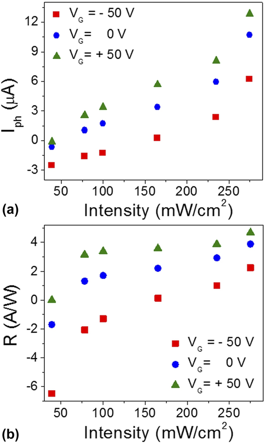
In addition to demonstrating the photoinduced p-to n-conversion of RGO/TSCuPc PTs, we characterized photocarrier generation properties. The effect of intensity and gate voltage on the photocurrent (I ph), defined as [I ph = I light − I dark], can be clearly seen in Fig. 6(a) where we plot the I ph as a function of light intensity for different gate voltages (V G = −50, 0, +50 V). At low light intensity (40 mW/cm2), the I ph is negative for V G = −50 and 0 V, while at +50 V, I ph is close to zero. As the light intensity increased to 80 mW/cm2, the I ph for V G = −50 V remained negative, while for V G = 0 V the I ph became positive. As the light is further increased to 165 mW/cm2, all of the I ph are positive. In addition, the I ph at higher V G is higher than the current at low V G. We obtained the maximum I ph = ∼ 13.5 μA at V G = 50 V for the light intensity of 275 mW/cm2. The current increases with increasing light intensity, indicating the photocarrier generation inside the RGO/TSCuPc films. Also, the changes (or increases) in current with varying gate voltage demonstrates a potential for signal amplification by the PT structure.
(a) I Ph versus light intensity of a RGO/TSCuPc phototransistor with different V G. (b) R versus light intensity of a RGO/TSCuPc phototransistor with different V G.

Photoresponsivity (R) is the critical parameters to evaluate the performance of a PT. Considering the geometry of the sample, R can be described by: R = I ph/P incLW, where P inc is the incident illumination intensity. Figure 6(b) shows the variation of R as a function of the intensity of light with three different values of V G (= −50, 0, and +50 V). R tends to increase nonlinearly with increasing light intensity. However, both positive and negative values of R were observed depending upon light intensity as well as V G. The negative values in R are reflected by negative I ph at low V G with low light intensity. At low light intensity (40 mW/cm2), R values are negative for both positive and negative V G, whereas for the intensity levels of 80 and 100 mW/cm2, R is negative for negative V G and positive for positive V G. For the intensity above 100 mW/cm2, R is positive for both positive and negative V G. We obtained the maximum R = 4.6 A/W at V G = +50 V for the light intensity of 275 mW/cm2.
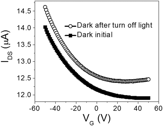
An important question in explaining the effect of light on RGO/TSCuPc PT is whether the light-induced p-to n-type conversion is reversible. We found that the p-to n-type switching behaviors are fully reversible. Figure 7 shows the I DS − V G characteristic of a device measured two hours after the light was turned off (open symbol). For comparison, we also present the original I DS − V G curve before the light was turned on. It can be seen that after the light is turned off, the device is converted back into the original p-type. There are slight increases in current, which may come from the photoreduction of RGO sheets.Reference Pei and Cheng56 When the light was turned on again, the same photoinduced n-type FET properties recurred, indicating that the p- to n-conversion originates from the light illumination.
I DS − V G curves of a RGO/TSCuPc device under the initial dark condition and the dark condition after taking measurements of 275 mW/cm2 light intensity.

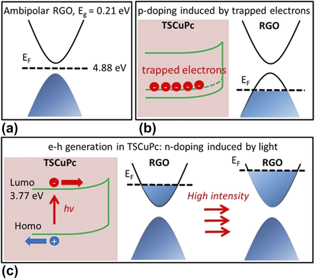
Our observations can be explained with the band diagram shown in Fig. 8. The RGO only FET shows ambipolar behavior when measured in an oxygen-free environment [the inset of Fig. 5(a)].Reference Joung and Khondaker14,Reference Joung, Chunder, Zhai and Khondaker43 The carbon sp 2 fraction of the RGO is 80% with an energy gap of 0.21 eV,Reference Joung and Khondaker14 while the Fermi energy of RGO is 4.88 eV.Reference Kong, Geng and Jung57 This is shown in Fig. 8(a). When TSCuPc molecules are anchored on the RGO sheets, in the absence of light, electrons are transferred from RGO to TSCuPc which were then trapped by TSCuPc at the TSCuPc/RGO interface, and the composite showed a p-type FET behavior [Fig. 8(b)]. This is consistent with the XPS data of RGO/TsCuPc hybrid presented in our previous publication where we observed that the C–C peak of RGO (284.6 eV) shift to 285.9 eV in RGO/TSCuPc, supporting the electron transfer from RGO to TSCuPc.Reference Chunder, Pal, Khondaker and Zhai24 On the other hand, under illumination, photogenerated excitons are produced in TSCuPc which are dissociated into electron–hole pairs at the TSCuPc/RGO interface. The electrons are donated (or transferred) from the lowest unoccupied molecular orbital level of TSCuPc (3.77 eV) to RGO, resulting in the n-type FET behavior [Fig. 8(c)].Reference Kong, Geng and Jung57
Energy level diagram of RGO and RGO/TSCuPc composite. (a) Ambipolar FET properties of the pure RGO sheet with an energy gap (E g) of ∼0.21 eV. (b) After anchoring of TSCuPc to RGO, electrons are transferred from RGO to TSCuPc in the dark resulting in a p-type behavior. (c) On photoexcitation of TSCuPc, electrons are transferred to the RGO, and holes in RGO sheets are quenched. As the light intensity further increased, more electrons contributed in transport, resulting in the n-type FET property.

The observed negative values for I ph and R at low light intensity and the increase of I ph and R with increasing light intensity can be explained as follows: In general, based on the operational principles, the decrease or increase of photoresponsivity (R) depends upon the rate at which the photocurrent (I ph) increases with incident power. The increase of photocurrent depends on several factors such as interface barriers and trap states of RGO. It has been pointed out that for p-type semiconductor composites, the electron transfer from donor molecules to a semiconducting layer can quench the p-type carrier (or holes mobility) resulting in a negative shift of V th and lowering of the hole mobility in the presence of light.Reference Zhang, Gan, Cao, Wang, Qi and Guo45,Reference Liu, Li, Shen, Cao, Guo, Zhang, Feng, Zhang, Liu, Steigerwald, Xu and Nuckolls58,Reference Zhang, Guo, Hui, Hu, Xu and Zhu59 Therefore, at low light intensity and low V G values, the photogenerated free electrons interact with the holes in RGO resulting in a lower hole mobility and hole current in our composite sample. This gives negative values of I ph and R. With increasing light intensity, the amount of photogenerated electrons increases and at some point, the photogenerated electrons become significantly larger than the trap (hole) states. This is also evident from the large increase in electron mobility from ∼0.018 to ∼0.083 cm2/Vs with an increase in intensity from 40 to 275 mW/cm2, while the hole mobility decreases from 0.095 to 0.022 cm2/Vs from dark to 40 mW/cm2 (no p-type conduction from 80 mW/cm2 and above). This results in a super-linear increase of I ph, hence an increase in R with intensity.
IV. CONCLUSIONS
We investigated the optoelectronic transport properties of the RGO/TSCuPc composite phototransistor. The synthesis of RGO/TSCuPc and formation of donor (TSCuPc)—acceptor (RGO) hybrid structure was confirmed by XRD and Raman spectroscopy. The p-type FET behavior in the dark was changed to an n-type under light illumination with a quenching of hole transport and an enhancement of electron transport. The device shows a very high photoresponsivity value that can be tuned by both the gate voltage and light intensity. Our study suggests that the photogenerated free electrons on TSCuPc molecules can be injected efficiently onto RGO sheets resulting in an increase in electron current and a hole quenching. The demonstration of high-performance RGO composite based PTs with majority carrier type conversion under visible light illumination is a significant step forward in realizing the overarching goals of RGO in optoelectronic applications.