Introduction
Modern wireless communication systems are rapidly evolving towards broader bandwidths and smaller form factors. In-band full-duplex (IBFD) technology, which allows simultaneous transmission and reception of signals at the same frequency, can significantly increase spectrum utilization and channel capacity, making it a major research focus. However, the strong signal from the transmission link can cause self-interference in the receive link through antenna coupling and other pathways. To ensure system sensitivity before the radio-frequency front end, high isolation must be achieved at the antenna level [Reference He and Li1]. To address this, various isolation techniques such as polarization diversity [Reference Hao, Cheng, Wu and Fan2, Reference Wang, Wei, Sun and Xie3], differential feeding [Reference Huang, Luo, Yan and Ma4], stacked patches [Reference Hu, Chen, Wu, Ye, Jiang, Li and Wu5], near-field cancellation [Reference Xie, Yao, Wei, Tang, Wang and Hu6], and defected ground structures [Reference Chen, Ding, Zhu and Liu7] have been proposed in the literature. Among them, the dual-polarized differential feeding structure, by utilizing both orthogonal polarization and common-mode suppression mechanisms, can significantly improve isolation without sacrificing radiation symmetry or cross-polarization performance. Additionally, it is easy to integrate with differential front ends or planar RF circuits.
Common dual-polarized antennas each have their own characteristics: Magneto-electric dipole antennas [Reference Tang, Ye, Zhu, Li and Wu8, Reference Xiang, Wu, Chen, Li, Ma, Xia, Yu, Jiang, Yu and Hong9] offer wide impedance bandwidth but have large sizes and high profiles; metasurface broadband antennas [Reference Chen and Yang10, Reference Liu, Yang, Chen, Zhang and Xiang11] provide advantages such as wide bandwidth, low profile, and low cost, making them suitable for broadband IBFD applications, but their many unit parameters and complex coupling make design and fabrication challenging; Fabry–Perot leaky-wave antennas [Reference Shahzadi, Comite, Kuznetcov and Podilchak12] offer high gain and thin profiles, but their bandwidth is narrow and lateral dimensions are large; dielectric resonator antennas [Reference Li, Huang, Tang, Ma, Zhang, Yang and Chen13, Reference Tang, Deng and Shi14] have high efficiency, large power capacity, and wide bandwidth in the millimeter-wave band, but the high εᵣ ceramic materials are costly and require strict processing accuracy; and dielectric patch antennas [Reference Wang, Tang, Yang and Chen15, Reference Zhang, Ke, Wang, Tang and Chen16] have high radiation efficiency, but their profile is larger than that of microstrip patch antennas, and their resonant frequency is sensitive to the dielectric constant εᵣ and manufacturing tolerances.
In contrast, microstrip patch antennas are most widely used in portable terminals due to their lightweight, low cost, and ease of integration with circuits, and their structure naturally supports differential feeding designs. Nevertheless, conventional structures face bandwidth limitations [Reference Zhang, Lv, Zhang, Wang, Zeng, Ding and Dai17]. In recent years, researchers have expanded the bandwidth of differential-fed dual-polarized microstrip patch antennas to 30–52% by incorporating techniques such as slot loading and parasitic patches [Reference Liu, Zhu, Zhang and Choi18–Reference Le and Ta24]. Some designs have also integrated filtering functions [Reference Sun, Zhai, Zhao, Lin, Zhang and Sun25, Reference Li, Huang, Hu, Chen and Yan26]; however, these solutions still commonly suffer from insufficient bandwidth, thicker profiles, or higher manufacturing costs.
To address these issues, this paper proposes a differential-fed dual-polarized microstrip patch antenna based on an FR4 substrate. The measured results demonstrate that the antenna achieves a 71.5% impedance bandwidth within the 4.06–8.58 GHz range, with a profile of only 0.086λL (where λL is the free-space wavelength corresponding to the lowest operating frequency), significantly outperforming existing similar designs. Additionally, the antenna exhibits high isolation between the two ports and low cross-polarization levels, fully validating its feasibility and practical value for IBFD applications, while the use of FR4 material keeps the overall manufacturing cost low.
Antenna design
Structure of antenna
The structure of the proposed fully symmetric dual-polarized dual-port antenna based on differential feeding is shown in Figure 1, which consists of two layers of FR4 dielectric substrates (εr = 4.4, tanδ = 0.02) and three metal layers. The top radiating structure is a rectangular patch (Patch1) with a slot, which is located at the junction between the green patch and the red cross-structure patch with a slot width S of 0.1 mm. The middle metal layer is a circular patch (Patch2), which is used for improving the impedance matching characteristics of the antenna at high frequencies. The ground plane is on the bottom. Four metallized vias function as coaxial feeding probes, constituting two pairs of differential ports: Pd 1 (P1/P3) and Pd 2 (P2/P4).
Structure of the proposed antenna: (a) perspective view, (b) Patch1, (c) front view, and (d) top view of the middle metal layer (size parameters: H1 = 3.2, H2 = 3.2, Wp = 12.8, Lst = 6.4, Wst = 3, S = 0.1, Rsub = 22, Rp = 2.8, Rf = 3.9, Rny = 19, Sr1 = 0.3, and Sr2 = 0.5 [unit: mm]).

Design of radiating patch
First, the differential S-parameters can be calculated by [Reference Eisenstadt, Stengel and Thompson27].
 \begin{equation}{S_{dd11}} = ({S_{11}} - {S_{12}} - {S_{21}} + {S_{22}})/2\end{equation}
 \begin{equation}{S_{dd22}} = ({S_{33}} - {S_{34}} - {S_{43}} + {S_{44}})/2\end{equation}
 \begin{equation}{S_{dd21}} = \left( {{S_{31}} - {S_{41}} - {S_{32}} + {S_{42}}} \right)/2\end{equation}
 \begin{equation}{S_{dd12}} = \left( {{S_{13}} - {S_{14}} - {S_{23}} + {S_{24}}} \right)/2\end{equation}
Since the antenna is of a fully symmetric structure, S 31 = S 32 and S 41 = S 42, and their coupling coefficients (Sdd 21 and Sdd 12) are theoretically zero [Reference Ta and Nguyen-Trong28]. Next, we will use the defined S-parameters to evaluate the performance of antenna structural evolution.
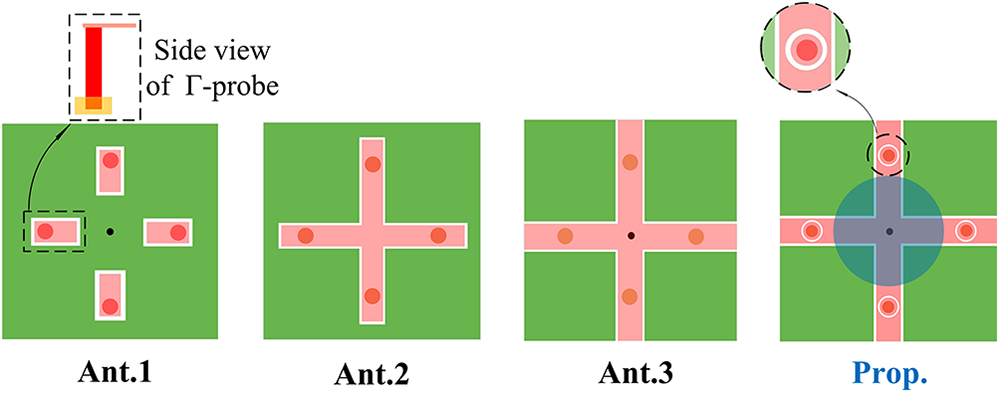
Figure 2 illustrates the structural evolution from the original structure (Ant. 1) to the proposed antenna. The initial design (Ant. 1) uses a traditional square patch (green area) combined with four small rectangular strips (pink area) separated by white slots whose width is S. Each small rectangular patch connects to a coaxial feed probe (marked by red circles), forming the Γ-probe. In Figure 2, a side view of the Γ-probe is shown above Ant. 1, where the red cylinder represents the coaxial feed probe, and the upper pink rectangular patch is the strip. Figure 3(a) shows the |Sdd 11| of Ant. 1 (with Γ-probe) and a typical square patch antenna with four differential probes (without Γ-probe). It can be seen that Ant. 1 can generate two resonant frequencies f 1 and f 3 and the Γ-probe design can significantly widen the bandwidth. According to the current distributions for f 1 and f 3 shown in Figure 3(b) and (c), at f 1, the dominant current is in-phase, exhibiting the TM10 mode. At f 3, the current distribution is even-symmetric along the x-axis and odd-symmetric along the y-axis, corresponding to the TM12 mode.
Design evolution of the proposed antenna configuration.

(a) |Sdd 11| of Ant. 1, (b) surface current at f 1, and (c) surface current at f 3.

Next, by extending the four Γ-probe-based strips into a pink cross structure, Ant. 2 is developed. This structure can introduce a new resonant point f 2 at 5.8 GHz, as shown in Figure 4(a). f 2 is directly affected by the length of the cross strips Lst, which means f 2 can shift to a lower frequency when Lst increases. At f 2, Figure 4(b) shows that the current is primarily concentrated within the interior and edges of the cross-shaped structure. The dominant current is in-phase, indicating that the TM10 mode is generated by the cross-shaped structure.
(a) |Sdd 11| of Ant. 2 under different Lst and (b) surface current at f 2.

We further extend the cross strips of Ant. 2 outward until they can truncate the green patch and Ant. 3 is created. This new structure can excite one more slot mode at f 4 (with current concentrated around the slot), as shown in Figure 5(a). Figure 5(a) also indicates that adjusting Wst (i.e., changing the position and length of the slot) can independently control the frequency of f 4. In addition, to solve the impedance mismatch of Ant. 3 at f 1, a circular slot ring (marked by the white circle) is etched at the feeding point to introduce a compensating capacitance, counteracting the inductive effect of the probe [Reference Hall29]. At this stage, the antenna (with an etched slot at the feeding probe) has a good impedance matching property at f 1 but that at high frequency f 4 needs to be optimized. f 4 corresponds to a slot mode generated by the gap between the patches. To optimize the impedance matching at f 4, a blue circular patch (Patch2) is added at the height H1 beneath the center of the patch to modify the magnetic and electric fields of the slot, thereby improving the impedance matching at f 4. This modification leads to the final design (Prop.). The performance of the two antennas is shown in Figure 6(a). We can clearly see that the operating bandwidth of Prop. antenna is effectively expanded by adding Patch2 to 71.5% (4.06–8.58 GHz). Additionally, the calculation for the input impedance of the differential-fed patch antenna can be expressed as [Reference Zhang and Wang30]. It is evident from Figure 6(b) that the impedance matching has been significantly improved after the circular slot ring is added.
(a) |Sdd 11| of Ant. 3 under different Wst and (b) surface current at f 4.

(a) |Sdd 11| and (b) input impedance of Ant. 3, Ant. 3 with etched slot and Prop.

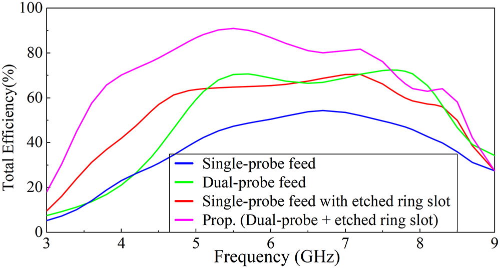
FR4’s high loss tangent can degrade the antenna’s efficiency. According to the previous studies, using a thicker FR4 substrate can mitigate this effect [Reference Nascimento, Lacava and Microstrip Antennas31, Reference Nascimento and Lacava32]. A low-cost probe-fed microstrip antenna using a 6.6 mm FR4 substrate can achieve nearly 75% radiation efficiency [Reference Nascimento, Lacava and Microstrip Antennas31]. However, these designs use a single-probe feed, which raises cross-polarization and adds inductive reactance. Efficiency is improved by adopting a dual-probe feed [Reference Petosa, Ittipibon and Gagnon33] and etching a capacitive ring slot near the probe(s) to compensate for the inductive reactance [Reference Hall29, Reference Nascimento, Mores, Schildberg and Lacava34], as shown in Figure 7.
Comparison of total efficiency for four different antenna configurations: single-probe feed, dual-probe feed, single-probe feed with etched capacitive ring slot, and the proposed design (dual-probe feed with etched capacitive ring slot).

Fabrication and measurements
Realization of differential feed
To meet the far-field radiation pattern testing requirements for broadband antennas, we adopt the 180° wideband power divider (WPD) [Reference Bialkowski and Abbosh35–Reference Ta, Nguyen, Nguyen, Ngoc and Trong37] as the differential feeding, as shown in Figure 8(a). It has a T-type architecture that combines slot line and microstrip transmission line, with an integrated microstrip-to-slot line broadband transition network. The simulated S-parameters of the designed WPD are shown in Figure 8(b), with |S 11| < −10 dB ranging from 3.5 to 8.5 GHz and balanced power distribution at the output ports (|S 21| = |S 31| = −3.9 ± 0.4 dB). In addition, the differential output ports (Port 2/Port 3) demonstrate a consistent 180° phase difference with phase variance within ±6° across the operational bandwidth.
(a) Geometry of the 180° WPD (unit: mm) and (b) simulated (Sim.) and measured (Mea.) S-parameters of the 180° WPD.

Measurements
To validate the proposed wideband dual-polarized microstrip antenna, we fabricated a prototype of the antenna, as shown in Figure 9(a). Nylon screws are used to fix the two-layer structure, and the RG402 coaxial cables are soldered to the four ports (P1–P4). The overall size of the antenna is 44 × 44 × 6.4 mm3. First, the S-parameters of the four antenna ports are measured. The differential S-parameters are then calculated using formulas (1), (2), (3), and (4) based on the measured S-parameters of the four ports. The simulated and measured differential S-parameters are presented in Figure 9(b). The simulated and measured results show good agreement, with the measured impedance bandwidth (|S₁₁| < −10 dB) reaching 71.5% (4.06–8.58 GHz) while port isolation remains above 42 dB throughout the operating band. Under Eq. (3) and Eq. (4), when the two cable lines connecting to the differential port are perfectly 180° out of phase, Sdd 21 and Sdd 12 are theoretically zero [Reference Ta and Nguyen-Trong28]. Thus, the inter-port isolation mainly depends on the phase matching of the cables between the antenna and the differential network.
(a) Antenna prototype and (b) simulated (Sim.) and measured (Mea.) S-parameters of antenna.

Next, similar to [Reference Wu, Guo, Zhu, Jiang and Ye36, Reference Ta, Nguyen, Nguyen, Ngoc and Trong37], the differential ports (Port 2/Port 3) of the WPD are connected to the antenna’s differential ports Pd 1 (P1/P3) or Pd 2 (P2/P4), as shown in Figure 10(a). After passing through the WPD, the signal is split into two differential signals that are directed to (Port 2/Port 3). The far-field radiation, gain and total efficiency of the antenna are then measured in a microwave anechoic chamber. The gain and total efficiency of the antenna within the operating frequency range are shown in Figure 10(b). The measured gain ranges from 3.5 to 8.2 dBi in the operating frequency band of 4.06–8.58 GHz, slightly lower than the simulation values. This small discrepancy may be caused by the fabrication and measurement errors.
(a) Far-field measurement environment and the antenna with feeding circuits and (b) realized gains and total efficiency of antenna.

Figures 11 and 12 show the radiation patterns of the antenna under the excitations at differential ports Pd 1 and Pd 2, respectively. By using the differential feeding scheme, the simulated cross-polarization levels (<−30 dB) are very low. Due to the presence of an asymmetric power divider, the measured cross-polarization levels are slightly higher than the simulated ones but they remain less than −20 dB across the operating frequency band.
The normalized radiation pattern of the antenna under excitation at differential port Pd 1.

The normalized radiation pattern of the antenna under excitation at differential port Pd 2.

Comparison and discussion
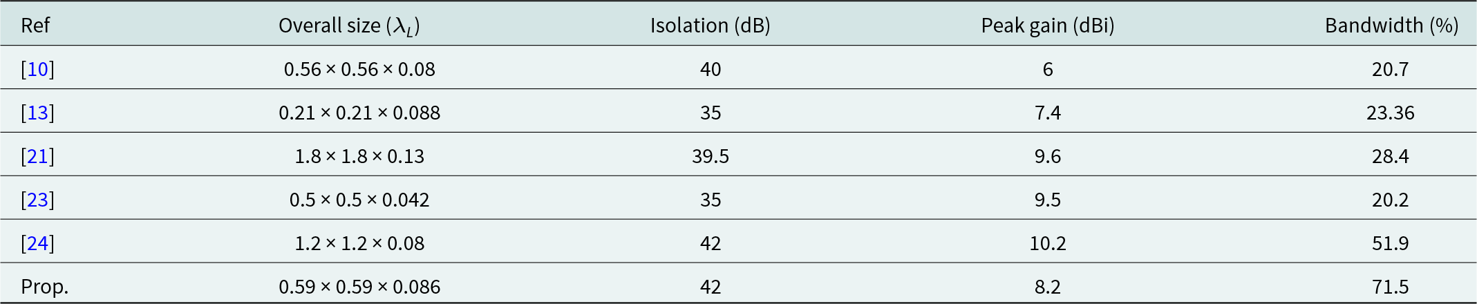
Table 1 compares the key technical parameters of the differential-fed dual-polarized antenna with some related researches. All of these designs can achieve high isolation between 35 and 52.5 dB by differential feeding and symmetric structures. Compared to other studies, the antenna proposed in this paper has a low profile with only 0.086λL, high isolation of 42 dB and broad bandwidth of 71.5% with relatively stable radiation characteristics, providing a promising solution for practical engineering IBFD applications.
Comparison of the differential-fed dual-polarized antennas with low-profile and broadband characteristics

Conclusion
This work presents a novel low-profile differentially fed dual-polarized patch antenna for IBFD systems, addressing the critical bandwidth-profile trade-off through two key innovations: (1) A four Γ-shaped probe feeding structure combined with a dual-layer patch configuration (featuring a cross-slotted upper patch for multi-resonance excitation and a middle circular patch for impedance matching), and (2) Systematic optimization of radiation elements. The implemented design achieves a 71.5% impedance bandwidth (4.06–8.58 GHz) with consistent port isolation >40 dB, while maintaining an ultra-thin 0.086λL profile. Experimental results verify 8.2 dBi realized peak gain with <−20 dB cross-polarization levels and stable directional radiation patterns. These advancements position the proposed antenna as a compact, cost-effective solution for emerging multi-standard systems, including 5G NR, Wi-Fi 6E/7, and next-generation full-duplex architectures.
Acknowledgement
This work was supported in part by the National Natural Science Foundation of China under Grants (62361008, 62261007) and in part by the Guizhou Provincial Basic Research Program (Natural Science) under Grant QKHJC MS [2025] 591.
Competing interests
The authors declare that they have no known competing financial interests or personal relationships that could have appeared to influence the work reported in this paper.

Jiahong Wu received a bachelor’s degree in communication engineering from Guizhou University, China, in 2023. Currently, he is pursuing a master’s degree at the Engineering Research Center of Power Semiconductor Device Reliability of the Ministry of Education, College of Big Data and Information Engineering, Guizhou University. His main research interest is broadband antenna designing.

Shixing Yu received a bachelor’s degree in electronic information engineering from the School of Electronic Engineering, Xidian University, China, in 2012. He obtained a PhD degree in electromagnetic fields and microwave technology from the same school at Xidian University, China, in 2017. Currently, he holds the position of Associate Professor at the College of Big Data and Information Engineering, Guizhou University, China. He has authored more than 30 research articles, and his current research interests include antennas and arrays, electromagnetic field theory, artificial electromagnetic structures, microwave devices, radio-frequency circuits, and microwave measurement.

Na Kou received a bachelor’s degree in electronic information engineering from the School of Electronic Engineering, Xidian University, China, in 2013. He obtained a PhD degree in electromagnetic fields and microwave technology from the same school at Xidian University, China, in 2018. Currently, he holds the position of Associate Professor at the College of Big Data and Information Engineering, Guizhou University, China. He has authored more than 20 research articles, and his current research interests include array antennas, conformal antennas, frequency-selective radar absorbers, wireless power transfer, and vortex electromagnetic fields.