Introduction
The semiconductor industry has been persistently seeking an ideal non-volatile memory (NVM) that can simultaneously possess attributes such as high density, high speed, low power consumption, and low cost.1 Charge-based flash memory represents the state-of-the-art NVM technology at present and is widely adopted in applications from embedded systems to portable electronics and mass storage because of its large capacity and inexpensive manufacturing.1–Reference Burr, Kurdi, Scott, Lam, Gopalakrishnan and Shenoy3 However, circumventing the problems associated with flash memory, such as limited endurance, slow write speed, and complicated data management schemes, has become more challenging as storage density increases. Moreover, density scaling through continued complementary metal oxide semiconductor (CMOS) scaling also faces several fundamental and technological challenges that will likely reach a limit below 20 nm. As an emerging memory technology, resistive random access memory (RRAM), which is based on a two-terminal device structure that stores data as a change in its resistance, has become a promising candidate due to its simple structure, fast programming, high stacking density, and facile fabrication.
The first true resistance switching devices were originally reported in the 1960s and involved oxides, including SiO2, sandwiched between a variety of metals in a metal/insulator/metal configuration. Most of the early work focused on unipolar switching in oxides. Systems exhibiting bipolar switching began to appear in the literature in the 1970s. In particular, resistive switching (RS) attributed to the formation and dissolution of an Ag filament in Ag-doped As2S3 was reported in 1976 by Hirose et al.Reference Hirose and Hirose4
We distinguish among three major types of RS behaviors depending on the switching mechanism.Reference Waser, Dittmann, Staikov and Szot5, Reference Waser and Aono6 One class is based on a unipolar thermochemical mechanism or memory effect in which a current-induced temperature increase leads to a fuse/antifuse process. The second class is based on the bipolar valence change mechanism or memory effect that occurs in several transition metal oxides and is triggered by the drift-diffusion of oxygen anions. Based on this class, the term “memristor”Reference Chua7 in a more general sense has been linked to RS effects,Reference Strukov, Snider, Stewart and Williams8 which led to an additional rise in interest in these emerging memory concepts. The third class, based on the bipolar electrochemical metallization mechanism or memory effect (ECM), relies on the electrochemical dissolution and deposition of active electrode metals such as Ag and Cu. This review will focus on these ECM cells, also called conductive bridging RAM (CBRAM) or programmable metallization cells (PMC) in the literature, which have seen tremendous advances recently in materials and device developments toward large-scale applications. For more extensive discussions on ECM cells, the reader is encouraged to consult a recent comprehensive review.Reference Valov, Waser, Jameson and Kozicki9
Device structure and material choices
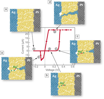
A basic ECM cell is a metal-solid electrolyte-metal system. Figure 1 sketches the operation principle of an ECM cell in conjunction with a current-voltage switching cycle using a quasi-static triangular voltage signal. The cell consists of an electrode made of an electrochemically active electrode (AE) metal, such as Ag or Cu, an electrochemically inert counter electrode (CE), such as Pt, Ir, or W, and a solid electrolyte layer sandwiched between the AE and CE.Reference Valov, Waser, Jameson and Kozicki9 In the initial high resistance state (OFF state) of the cell, no electrodeposit of the AE metal is present on the CE (Figure 1a).
Schematic of the (a–d) SET and (e) RESET operations of an electrochemical metallization (ECM) cell. Reprinted with permission from Reference Reference Valov, Waser, Jameson and Kozicki9. ©2011, IOP Publishing.

A SET (or programming) process occurs if a sufficient positive bias voltage is applied to the AE. The overall SET process involves the following steps, using Ag as an example of the AE and Pt as the CE:Reference Waser, Dittmann, Staikov and Szot5, Reference Waser and Aono6, Reference Valov, Waser, Jameson and Kozicki9
1. Anodic dissolution of Ag according to the reaction

where Ag+ represents the monovalent metal cation, the most common oxidation state of Ag, in the solid electrolyte;
2. Drift of the Ag+ cations across the solid electrolyte under an applied high electric field;
3. Reduction and electro-crystallization of Ag on the surface of the Pt according to the cathodic deposition reaction
(2)

4. Growth of the Ag filament.
The electro-crystallization process (Equation 2) leads to the formation of a metal filament growing preferentially toward the AE (Figure 1c). After the metal filament has grown to make an electronic (e.g., galvanic) contact with the AE, the cell has switched to the ON state (Figure 1d). The cell retains the ON state unless a sufficient voltage of opposite polarity is applied and the electrochemical dissolution of the metal filament RESETs the cell (Figure 1e) to its initial OFF state (Figure 1a).
In general, different switching parameters (e.g., a higher switching voltage) are typically required to switch a virgin cell for the first time in a process that is normally termed electroforming or forming. It is conceivable that the initial electroforming process causes structural changes to the electrolyte layerReference Waser, Dittmann, Staikov and Szot5, Reference Waser and Aono6 and allows subsequent resistance switching to occur at lower voltages. For example, for an SiO2 electrolyte, it has been suggested that during electroforming, a growing filament in SiO2 will impose mechanical stress and form nanoscale conduction channels for metal cations, which persist after electrochemical dissolution of the original filament (e.g., Figure 1e).Reference Schindler, Staikov and Waser10 Such a channel could then form the template for subsequent switching events. Details of the forming process, however, may vary significantly depending upon electrolyte materials and cell geometries.
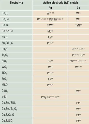
A vast number of combinations of materials fit this basic description of ECM cells, and indeed a wide variety of materials have been explored for use as ECM materials. Table I provides a summary of several material combinations that have been investigated over the past 30 years. Over the past 10 years of research, an extraordinary variety of insulating materials have been utilized as electrolyte layers, even materials not traditionally viewed as good solid electrolytes, such as SiO2. One reason for this is that the electrolyte can be made very thin, meaning ions from the AE do not have to travel far to form a filament. Thus, even poor ionic conductors can switch quickly, owing to the high electric fields that even modest applied voltages can produce.
Summary of reported electrochemical metallization cells employing either Ag or Cu as an active electrode (AE) metal and various electrolytes and counter electrode (CE) metals.
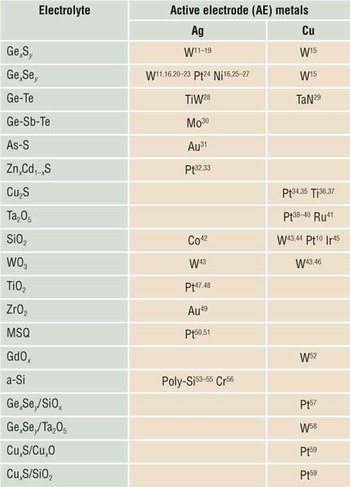
Electrolyte and CE materials are indicated in each row. For bilayer electrolytes, AE would be placed to the left of the electrolyte (e.g., Cu/A/B/Pt for a cell with a Cu AE metal and A/B bilayer electrolyte). Information compiled by John R. Jameson, Adesto Technologies Corp. Reprinted with permission from Reference Reference Valov, Waser, Jameson and Kozicki9. ©2011, IOP Publishing.
Since the source/sink of the ions form a filament, the choice of AE is critical for the operation of ECM cells. Far fewer AE materials have been investigated than CE, as seen in Table I, due to the fact that a narrow window in the electrochemical potential exists for easy redox reactions. The choice of Ag as the AE material in early ECM cellsReference West, Sieradzki, Kardynal and Kozicki60, Reference Kozicki and West61 was motivated by the use of AsxSy and related higher chalcogenide electrolytes, which had been extensively studied as prototypical Ag+ conductors. Nowadays, Cu is also commonly studied as an AE material. Recently, alloys such as CuTe have also been explored as alternative AE materials instead of elemental metals.Reference Aratani, Ohba, Mizuguchi, Yasuda, Shiimoto, Tsushima, Sone, Endo, Kouchiyama, Sasaki, Maesaka, Yamada and Narisawa52
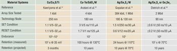
The choice of CE material has been driven by the rather straightforward requirements that the CE should be sufficiently inert (i.e., no electrochemical dissolution should occur during RESET operation) and that it be compatible with future large-scale fabrication. The latter requirement is of lesser concern for fundamental research, making Pt a common choice in university laboratories. At the industrial level, W is seen as a natural choice, as standard processes already exist for manufacturing W vias.Reference Symanczyk, Bruchhaus, Dittrich and Kund12, Reference Gopalan, Ma, Gallo, Wang, Runnion, Saenz, Koushan, Blanchard and Hollmer19, Reference Kund, Beitel, Pinnow, Rohr, Schumann, Symanczyk, Ufert and Muller23 For ECM arrays employing some of the materials combinations listed in Table I and utilizing the 1T1R (one transistor for device selection and one RS element) architecture, key performance data are summarized in Table II.
Summary of key performance data reported to date in electrochemical metallization arrays.

All arrays utilized 1T1R (one transistor for device selection and one resistive switching element) architecture. Compiled with information from ChenReference Chen62 with the addition of data recently reported for Ag/GexSy/W cells.Reference Gopalan, Ma, Gallo, Wang, Runnion, Saenz, Koushan, Blanchard and Hollmer19
Electrochemistry and kinetics of ECM
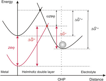
ECM switching speed can be limited by the kinetics of the redox reactions of the AE material at either the anode or the cathode, or by the kinetics of cation transport through the electrolyte layer. The measure for constrictions in the electrode reaction rate is the overpotential (Δφ), defined as the deviation of the potential from that at equilibrium. What determines the electrode reaction (Mz – + zc– ↔ M) is the overpotential ΔφH assigned to the Helmholtz double layer at the electrolyte/electrode interface, as shown in Figure 2. ΔφH can be assigned to the initial crystallization process Δφcrystal and the charge transfer process through the Helmholtz double layer Δφcharge, and thus ΔφH = Δφcrystal + Δφcharge. The initial crystallization can be observed mainly for reversible processes and generally at lower overpotentials (up to roughly 50 mV). Details on the effects of the crystallization overpotential on the ECM cell performance are given in Reference Reference Waser, Dittmann, Staikov and Szot5.
Free energy diagram of a charge transfer process. The black curves represent the initial state, and the red curve results after applying an electric potential to the metal electrode. OHP is the outer Helmholtz plane.  ,
 ,
 , and
 represent the activation free energy for the forward and backward reactions without and with an applied voltage, respectively. Reprinted with permission from Reference Reference Valov, Waser, Jameson and Kozicki9. ©2011, IOP Publishing.

The free energy of the oxidized state of the redox reaction (i.e., Mz + + ze–, where Mz + and ze– are separated by the Helmholtz double layer) is shifted by zeΔφcharge because the electrochemical potential of the electrons changes by the same amount, Δφcharge. However, the free energy of the reduced state (i.e., M) is not affected by Δφcharge due to its charge neutrality. Therefore, the formation free energy of the reaction, Mz + + ze– ↔ M, as well as the activation barrier height is given by a function of Δφcharge.
The Faradaic current versus voltage relationship for this redox reaction controlled by charge transfer at steady state conditions is given by the Butler-Volmer equation:

where i is the Faradaic current density; i 0 is the exchange current density; α is the transfer coefficient; and zi is the number of exchanged electrons. The first term on the right side of Equation 3 denotes the anodic process (oxidation),  , and the second term the cathodic process (reduction)
 . The exchange current density defines the current density at equilibrium where the Faradaic current is zero. The Butler-Volmer equation is derived for a single step electron transfer case and does not account for additional effects (e.g., multi-step processes, double layer effects). However, for the description of the ECM cells of monovalent cations (e.g., Ag+), no other terms are needed in the equation.
Unlike liquid electrolytes containing a high concentration of mobile ions with high mobility, the diffuse double layer may not be present in the solid electrolyte of ECM cells; the solid electrolyte may be much thinner than the electric field screening length corresponding to the diffuse double layer thickness. In this case, cation drift by an internal electric field, rather than diffusion, plays a role in the migration of cations. Note that the diffusion direction is opposite to the drift so that it leads to depolarization. The drift-diffusion theory for ions is well described for bulk materials that are regarded as ideally diluted solutions under a small electric field satisfying a first-order approximation. However, ECM cells may not satisfy this condition. High electric fields due to the very thin electrolyte layer and high concentration of dissolved cations may make the unmodified drift-diffusion theory not suitable for the description of ECM cells. Exponential dependence on the electric field similar to Equation 3 has been observed experimentally.Reference Schindler, Staikov and Waser10, Reference Russo, Kamalanathan, Ielmini, Lacaita and Kozicki13, Reference Kozicki, Park and Mitkova25, Reference Banno, Sakamoto, Hasegawa, Terabe and Aono34, Reference Jo, Kim and Lu64, Reference Terabe, Hasegawa, Nakayama and Aono65
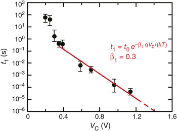
The kinetics of the filament formation process and corresponding SET switching speed can be limited by the following factors that are of series contributions: (1) the anodic dissolution of the AE; (2) the migration of the metal ions through the electrolyte; (3) the reduction of the ions to metal at the CE (limited by charge transfer, drift-diffusion, or crystallization); and (4) the filament growth. It is estimated that anodic dissolution may be a fast process due to the high electric fields ensuring sufficient decrease of the energy barrier maximum, shown in Figure 2 at the anode interface. Another approach models the anodic dissolution as the rate-limiting step and deduces an exponential rate dependence.Reference Jameson, Gilbert, Koushan, Saenz, Wang, Hollmer and Kozicki66 Concerning process (2), metal ion migration can be the rate-determining factor depending on the diffusion coefficient or mobility of the electrolyte used, though the electrolyte is very thin. For instance, filament formation in several insulators of low diffusion coefficients of extrinsic cations (e.g., SiO2, amorphous Si, Ta2O5, WO3) may be limited by process (2). The exponential dependence of the SET speed on voltage, as shown in Figure 3, might reflect the exponential field-dependence of the underlying ionic migration, as several studies have suggested, despite the fact that an evaluation of the corresponding equation typically leads to unrealistically large ion hopping distances. The metal deposition process at the CE (i.e., process 3) is likely to be the slowest process, as it is also related to space expansion due to new phase formation, which strongly suppresses the electro-crystallization rate and, in turn, limits the growth rate of the filament. According to a study on Ag-GeSe systems by means of potentiodynamic methods,Reference Schindler, Valov and Waser67 the reduction of Ag ions at the CE determines the overall reaction rate and, therefore, the switching speed during the SET process in this system.
Exponential dependence of the SET speed, t 1, on the SET voltage, V C. Device structure was Ag/GexSy/W. Reprinted with permission from Reference Reference Russo, Kamalanathan, Ielmini, Lacaita and Kozicki13. ©2009, IEEE.

It follows from the discussion that all three stages, processes (1–3), during filament formation can be the rate-limiting process under any given experimental conditions, so that it is difficult to offer a universal answer. Therefore, one should carefully go through each process for the system under investigation and compare the rate of each process in order to answer the question about the rate-limiting process.
Implications for device performance
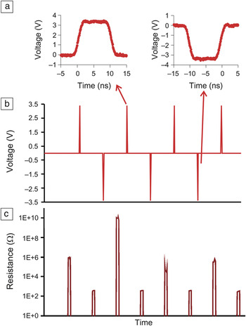
RS in ECM cells can take place in the ns (nanosecond) range with only a few volts of applied voltage.Reference Meier, Schindler, Gilles, Rosezin, Rudiger, Kugeler and Waser50, Reference Aratani, Ohba, Mizuguchi, Yasuda, Shiimoto, Tsushima, Sone, Endo, Kouchiyama, Sasaki, Maesaka, Yamada and Narisawa52 This implies that the dissolution and electro-crystallization occur at the ns scale. An example is a Pt/MSQ/Ag/Pt ECM cell with 100 nm line width reliably programmed with 10 ns, ±3.5 V write/erase voltage pulses, as seen in Figure 4. Moreover, the programming current of ECM cells has been shown to be as low as a few nA.Reference Schindler, Weides, Kozicki and Waser45 In contrast, the requirement of the retention performance of ECM cells as an NVM dictates that the device maintains its state for about 10 years with minimal read disturbance. Because the read voltage, limited by the thermal voltage (∼26 mV at room temperature), cannot be much smaller than approximately one-tenth of the programming voltage, the rate-limiting processes in ECM cells must still be sufficiently nonlinear in order to meet the change of ∼16 orders of magnitude in time scales from ns during programming to 10 years retention for reading. This “voltage-time dilemma”Reference Waser, Dittmann, Staikov and Szot5 in practice places a restriction on screening out potential NVM devices. Fortunately, it has been shown that the rates of metal dissolution and crystallization have exponential dependence on applied voltages, making it possible to overcome the voltage-time dilemma in ECM cells. In this case, it is desirable to choose materials with high energy barriers for charge transfer, which favors long retention. The loss in speed can be compensated by using high programming electric fields to take advantage of the exponential speed up. However, since the decisive rate-limiting processes in individual ECM systems may be different, careful analysis needs to be performed for different systems to achieve device optimizations in light of overcoming the voltage-time dilemma.
Pulse measurements on a Pt/MSQ/Ag/Pt electrochemical metallization (ECM) cell. (a) Shape of applied voltage pulses, (b) series of pulses, and (c) the measured resistance. Reprinted with permission from Reference Reference Russo, Kamalanathan, Ielmini, Lacaita and Kozicki13. ©2009, IEEE.

The retention of the ON (SET) state is a critical issue, whereas the OFF (RESET) state of ECM cells is quite stable over long periods of time, even at elevated temperatures.Reference Symanczyk, Bruchhaus, Dittrich and Kund12, Reference Kund, Beitel, Pinnow, Rohr, Schumann, Symanczyk, Ufert and Muller23, Reference Kaeriyama, Sakamoto, Sunamura, Mizuno, Kawaura, Hasegawa, Terabe, Nakayama and Aono37 An interesting observation (e.g., References Reference Symanczyk, Bruchhaus, Dittrich and Kund12 and Reference Russo, Kamalanathan, Ielmini, Lacaita and Kozicki13 for Ag/GexSy/W cells) is that the retention of the ON state improves as the value of R ON decreases. An explanation pointed out by several authorsReference Russo, Kamalanathan, Ielmini, Lacaita and Kozicki13, Reference Kamalanathan, Russo, Ielmini and Kozicki14 is that lower values of R ON correspond to thicker, or perhaps multiple, metal filaments, which would presumably be slower to “erode” away. This implies that the retention of ECM cells depends on the SET/RESET algorithm that is used, as R ON depends strongly on factors such as the current compliance used for SET.
Scaling potential, integration, and prospects
ECM cells are considered to be highly scalable devices, owing to the fact that current in the ON state is presumably carried by a very narrow filament. The key piece of evidence normally cited for scalability is that the resistance of the ON-state does not depend, or depends only weakly, on the area of the device. The excellent scalability of ECM cells has been demonstrated directly in a number of studies (e.g., 30 nm in diameter for Cu2S-based cellsReference Sakamoto, Banno, Iguchi, Kawaura, Sunamura, Fujieda, Terabe, Hasegawa and Aono36 and 20 nm for GexSey-basedReference Kund, Beitel, Pinnow, Rohr, Schumann, Symanczyk, Ufert and Muller23 and GdOx-basedReference Aratani, Ohba, Mizuguchi, Yasuda, Shiimoto, Tsushima, Sone, Endo, Kouchiyama, Sasaki, Maesaka, Yamada and Narisawa52 cells). Furthermore, in particular Pt/Ag2S/Ag/Pt crossbar cells, it has been shown that the ON resistance can be controlled down to quantum conductance levels (2e 2/h) and changed in discrete steps. Observations of the quantum conductance steps suggest that ECM cells could be scaled down to the true atomic level.Reference Terabe, Hasegawa, Nakayama and Aono65, Reference Jameson, Gilbert, Koushan, Saenz, Wang, Hollmer and Kozicki66
ECM cell arrays can be active, utilizing a transistor to access each memory cell, or passive, in which each cell has a diode-like device in series with the storage element to provide cell-to-cell isolation. Active arrays, in which each cell contains one transistor for device selection and one RS element (1T1R), have been demonstrated by various groups.Reference Gopalan, Ma, Gallo, Wang, Runnion, Saenz, Koushan, Blanchard and Hollmer19, Reference Gilbert and Kozicki21 The area of an individual cell in the 1T1R approach is governed in this case not by the storage element but by the select transistor area, which is typically 8F 2 to 6F 2 (where F is the minimum feature size) if DRAM select transistors are used. A second drawback to the 1T1R approach is that the transistors have to be fabricated in the Si substrate, making it difficult to achieve multilayer stacking of the cells for higher storage densities.
A diode-isolated passive array, in which each cell contains one RS element and one diode (1D1R) as the selection device, is a more compact alternative than the 1T1R approach.Reference Kim, Jo, Gaba and Lu55, Reference Lee, Seo, Kim, Ahn, Seo, Yoo, Baek, Kim, Byun, Kim, Hwang, Kim, Jeon and Park68–Reference Puthentheradam, Schroder and Kozicki72 The diode plays a role in preventing so-called sneak currents through unselected cells in the network. Zener or breakdown diodes rather than conventional PN diodes are compatible with ECM cells, which require bipolar applied signals for SET/RESET.Reference Puthentheradam, Schroder and Kozicki72 The main advantage of the 1D1R approach is that it may achieve a design rule of 4F 2, much smaller than the 1T1R scheme, and enables multi-stacking memory arrays. However, the fabrication of compatible integrated diodes has been a significant challenge.
A different approach to overcome the sneak path problem and to operate large passive crossbar arrays is based on complementary resistive switches (CRS),Reference Linn, Rosezin, Kugeler and Waser73 as briefly mentioned in the introductory article. In CRS, each memory cell is composed of two anti-serial (complementary) interconnected ECM cells but with no additional selection devices.Reference Linn, Rosezin, Kugeler and Waser73 It is worthwhile noting that since no additional transistors or diodes are required, the CRS approach can be highly scalable. The internal operation of ECM-based CRS cells has been confirmed experimentally,Reference Rosezin, Linn, Nielen, Kuegeler, Bruchhaus and Waser74 and an interactive demonstration is available online.75
With the many merits discussed previously, ECM memory is a leading candidate for next generation NVM, potentially replacing existing charge-based Flash and DRAM memories as a universal memory technology. Looking into the future, further advances will be required to address the temperature tolerance issue of some electrolyte materials and demonstrate the retention robustness when the filament is further scaled to the (several) nm regime.
Further outlook for applications of ECM cells
Beyond applications in high-density memory for data storage, electrochemical metallization (ECM) devices have attracted interest in a broad range of applications such as non-volatile standard random access memory (SRAM),Reference Wang, Gibby, Wang, Chen, Fujita, Griffin, Nishi and Wong76 reconfigurable logic, and neuromorphic systems. A non-volatile SRAM is expected to effectively reduce standby power consumption presently observed in conventional SRAM cells by storing the state information in a pair of resistive switching cells, such as ECM cells.Reference Wang, Gibby, Wang, Chen, Fujita, Griffin, Nishi and Wong76 ECM cells can also be used as switchable interconnects in reconfigurable large-scale-integration circuits, such as field programmable gate arrays.Reference Kaeriyama, Sakamoto, Sunamura, Mizuno, Kawaura, Hasegawa, Terabe, Nakayama and Aono37, Reference Sakamoto, Lister, Banno, Hasegawa, Terabe and Aono39, Reference Strukov and Likharev77
The structure and performance of the ECM cells bear many resemblances with those of a synapse—the interconnection between neurons in biological creatures, in the sense that they are both “two-terminal” devices whose resistance can be modified by stimuli applied across them.Reference Swaroop, West, Martinez, Kozicki and Akers78 Several recent studies have attempted to build brain-inspired computing systems by using a crossbar network of ECM cells acting as synapses.Reference Jo, Chang, Ebong, Bhadviya, Mazumder and Lu79, Reference Ohno, Hasegawa, Tsuruoka, Terabe, Gimzewski and Aono80 Compared to conventional CMOS-based logic circuits, the bio-inspired computing approaches offer much better scaling potential and energy efficiency when dealing with complex tasks and, along with memory, can be a main driver for continued material and device development of ECM cells.
Acknowledgments
W.L. would like to thank Dr. Yuchao Yang for his help and the National Science Foundation CAREER award (ECCS-0954621) for partial financial support. D.S.J. would like to acknowledge a KIST research grant (grant no. 2E22123). The authors appreciate the careful consistency check and symbol check by Stefan Tappertzhofen, RWTH Aachen University.