I. INTRODUCTION
One-dimensional (1D) nanostructures, such as semiconducting and metallic nanowires (NWs), nanobelts, and carbon nanotubes, have attracted substantial attention because of their unique electrical, optical, mechanical, and thermal properties and their potential utility in a wide variety of nanoelectronic and optoelectronic applications. Semiconducting and metallic 1D nanomaterials fabricated from bottom-up synthesis approaches can be used as fundamental building blocks for nanoscale devices and circuits and may have the potential to replace certain conventional top-down processes. In particular, silicon-based NWs may be an attractive alternative to conventionally processed Si-based devices if their intrinsic self-assembly can be harnessed for effective device fabrication. In addition, silicon-based NWs can potentially function as the switch (i.e., transistor), insulator (silicon oxide), and local interconnect (e.g., metal silicide NW) to form an inherently integrated nanoelectronic system—potentially on the same self-assembled nanostructure.Reference Morales and Lieber1–Reference Wu, Xiang, Yang, Lu and Lieber4
Currently, several methods are available to synthesize silicon-based NWs including laser ablation,Reference Morales and Lieber1, Reference Zhang, Tang, Wang, Yu, Lee, Bello and Lee5 physical vapor deposition (PVD),Reference Zakharov, Werner, Gerth, Schubert, Sokolov and Gösele6 thermal evaporation,Reference Yu, Bai, Ding, Hang, Zhang, Wang, Zou, Qian, Xiong, Zhou and Feng7 and chemical vapor deposition.Reference Westwater, Gosain, Tomiya, Usui and Ruda8–Reference Hochbaum, Fan, He and Yang10 In the literature, these methods have been roughly categorized according to the underlying growth modes described, respectively, as solid–liquid–solid (SLS) growth,Reference Paulose, Varghese and Grimes11, Reference Yan, Xing, Hang, Yu, Wang, Xu, Xi and Feng12 vapor–liquid–solid growth,Reference Wagner and Ellis13, Reference Givargizov14 and oxide-assisted growth (OAG).Reference Zhang, Lifshitz and Lee15–Reference Zhang, Chu, Cheung, Wang and Lee17
The SLS growth approach is a relatively straightforward technique to synthesize silicon-based NWs because it does not require a gas phase precursor such as SiH4 or SiCl4. SLS-grown NWs typically exhibit an amorphous structure and can incorporate nonstoichiometric amounts of oxygen. Consequently, they are often referred to as silica NWs or amorphous silicon NWs.Reference Paulose, Varghese and Grimes11, Reference Yan, Xing, Hang, Yu, Wang, Xu, Xi and Feng12 NWs can be directly grown on a silicon substrate via the SLS process, which acts as the silicon source.Reference Paulose, Varghese and Grimes11 In the SLS process, a thin metal catalyst film (typically Au) is deposited on a single-crystal silicon substrate. The annealing of the catalyst-coated Si substrate results in metal–silicon alloy nanodroplet formation. Continuous diffusion of silicon atoms from the substrate to the droplet at elevated temperatures causes saturation of silicon atoms inside the alloy droplet, which leads to precipitation of silicon at the surface of the droplet to form a Si NW growth front.Reference Paulose, Varghese and Grimes11
In most SLS NW studies, experimental analysis has centered on Au–Si alloy nanoparticles at the onset of the SLS growth process and/or on fully formed NWs following prolonged SLS annealing or growth cycles.Reference Paulose, Varghese and Grimes11, Reference Yan, Xing, Hang, Yu, Wang, Xu, Xi and Feng12, Reference Lee, Rogers, Carpenter, Eisenbraun, Xue and Geer18–Reference Kim, An, Woo and Yoon20 However, detailed investigations of SLS germination of NWs from catalyst particles have faced experimental challenges associated with observing the very early stages of the SLS NW growth process due to nature of the high temperature processing. It is difficult to rapidly quench or halt the SLS growth process owing to the configuration of typical annealing systems or reactors wherein the time lag between temperature setpoint control and chamber response extends by several minutes the time for which the chamber remains at temperatures sufficiently high for SLS NW growth.
In this work, an emphasis was placed on the initial nucleation and formation of SLS silica NWs to further investigate early-stage growth modes. Specifically, the sample position within the SLS NW growth chamber and the ramp rates of inert gas flow within the chamber during NW growth were varied to controllably quench SLS NW formation early in the growth process. As a result of this approach, a previously unreported, high temperature SLS silica NW growth mode has been observed and investigated. In this novel mode, SLS NW nucleation and subsequent growth was uniquely promoted by—and coupled to—the formation of thermally etched pyramidal pits in the Si substrate, which formed during the high temperature anneal phase before the onset of SLS NW formation. The silicon oxide-mediated thermal pit formation process enhanced Si transport at the pyramidal pit faces to Au–Si alloy droplets directly adjacent to the pits. Consequently, SLS NW nucleation and growth was preferentially promoted at the pit edges. The promotion of SLS NW growth by the pyramidal pits resulted in the observation of SLS NW “blooms” at the pit locations. Subsequent NW growth—occurring both at the pit sites and, subsequently, from Au–Si alloy droplets distributed across the planar surfaces of the Si wafer—eventually occluded the pits complicating experimental observation of this mode. This newly observed process is termed as “thermal pit-assisted growth.”
The observation of void formation in Si systems exhibiting SLS growth has been noted in the literature. It had been previously observed that Si-based NWs can nucleate from alloy droplets inside irregular voids on the silicon substrate surface—irregular voids that had been created by the inflow of the silicon to the alloy droplet.Reference Paulose, Varghese and Grimes11, Reference Sekhar, Ramgir, Joshi and Bhansali19 Irregular Si void formation was also reported during silicon oxide NW growth from pyrolysis of a polyimide (PI) thin film in an Au nanoparticle/PI/Si thin film stack at 1000 °C.Reference Kim, An, Woo and Yoon20 In this work, the formation of the SiOx NWs was sustained by the oxygen derived from carbonization of the polyimide thin film, whereas Si was provided from the substrate.Reference Kim, An, Woo and Yoon20 There was some evidence of very small pyramidal pit formation in Ref. Reference Kim, An, Woo and Yoon20, in the NW growth region, although no conclusions were drawn regarding their relation to silica NW growth. These observations are substantially distinct from the work presented here wherein the formation of large-scale pyramidal pits in the Si was observed before silica NW nucleation and served to promote silica NW growth.
The remainder of this work reviews the experimental methodologies for these investigations and presents morphological and compositional analyses for determination of Au–Si alloy droplet disposition with respect to the pyramidal pits. A schematic outline of the thermal pit-assisted growth mode is also presented and discussed.
II. EXPERIMENTAL METHODS
For SLS NW synthesis, p-type (100) silicon wafers with electrical resistivity in the 1–20 Ω·cm range were used. Wafers were cleaned with diluted hydrofluoric acid (5%) to remove the native oxide layer and ultrasonicated in acetone to remove organic contamination. The cleaned samples were immediately loaded into a PVD chamber (evacuated to 5 × 10⁻⁷ Torr) for sputtering of an Au catalyst film with a thickness of 4 nm for SLS growth.
Following Au deposition, the silicon samples were placed inside an annealing chamber. The annealing chamber was evacuated to a base pressure of ∼5 Torr and backfilled to atmospheric pressure with high purity (99.999%) Ar gas. For conventional SLS NW growth, the Au-deposited Si samples were annealed at 1000 °C (30 min ramping time) under Ar (also 99.999% purity) gas flow at 2000 sccm. The annealing duration was varied from 10 to 120 min after the temperature ramp to investigate the effect of annealing time on the Si NW diameter, length, and overall morphology.
To investigate the early stages of SLS NW growth, a shorter annealing duration (typically, below 15 min) was utilized. However, on disengaging the chamber-heating elements, the sample continued to undergo a latent annealing duration of ∼8 min, while temperature cooled to ∼800 °C. To eliminate this unnecessary duration and to enhance investigation of the early stages of NW growth, 20,000 sccm of Ar was flowed inside the chamber, which quenched the SLS NW growth on the order of tens of seconds.
Structural and compositional properties of SLS NWs synthesized via the conventional SLS process and the rapidly quenched SLS process were analyzed using scanning electron microscopy (SEM), SEM-based energy dispersive x-ray spectroscopy (EDS), transmission electron microscopy (TEM), and TEM-based selected area electron diffraction (SAED). EDS analysis utilized a 10-kV electron beam leading to a probe depth range in c-Si of ∼0.9 μm. The lateral spatial resolution for elements confined to the surface is expected to be substantially lower.
III. EXPERIMENTAL QUENCHING OF SLS SILICA NW GROWTH
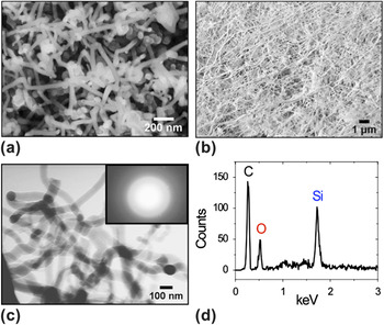
SEM images of SLS NWs synthesized via the conventional (slow quench) growth mode for various-length anneals at 1000 °C are shown in Fig. 1. The furnace temperature was ramped to 1000 °C for 30 min under 2000 sccm Ar flow. After the ramp, the furnace temperature was held constant for the durations of 15 and 90 min. SEM images of SLS NWs grown under these conditions are shown in Figs. 1(a) and 1(b), respectively. In agreement with the earlier studies, extended annealing time resulted in increased NW coverage of the substrate and more extensive development of a wire-like morphology.Reference Paulose, Varghese and Grimes11, Reference Yan, Xing, Hang, Yu, Wang, Xu, Xi and Feng12, Reference Lee, Rogers, Carpenter, Eisenbraun, Xue and Geer18–Reference Kim, An, Woo and Yoon20
Scanning electron microscopy (SEM) images of solid–liquid–solid (SLS) nanowires (NWs) synthesized at 1000 °C for anneal durations of (a) 15 min and (b) 90 min. The former is at a higher magnification to show the detail of early-stage growth. (c) Transmission electron microscopy images of SLS-grown NW for anneal duration of 90 min. Inset shows selected area electron diffraction pattern. The camera length was 100 cm. (d) Energy dispersive x-ray spectroscopy (EDS) image of NW. Si and O are the primary elements detected. The SEM-EDS was performed on a highly oriented pyrolytic graphite substrate. The carbon peak is due to the substrate.

Transmission electron microscopy (TEM) and SEM-based EDS were used to carry out structural and compositional analyses of conventionally grown SLS NWs [Fig. 1(c)]. NWs were detached from the initial silicon wafer using ultrasonication in methanol solution. SAED patterns were acquired from an individual NW and indicated a locally amorphous structure. The EDS spectra of an as-deposited single NW on highly oriented pyrolytic graphite substrates indicated the presence of oxygen [Fig. 1(d)] and implied that the NWs are likely SiOx in nature, consistent with the observation of an amorphous microstructure. This is expected for SLS NW growth and agrees with earlier studies.Reference Paulose, Varghese and Grimes11, Reference Yan, Xing, Hang, Yu, Wang, Xu, Xi and Feng12, Reference Lee, Rogers, Carpenter, Eisenbraun, Xue and Geer18–Reference Kim, An, Woo and Yoon20
Central to the investigation of the early stages of SLS NW growth was the ability to differentially quench NW growth across the sample for comparative SEM image and SEM-EDS analysis. As noted above, quenching was achieved by positioning Au-deposited samples near the chamber’s Ar gas inlet (as compared to the center of the annealing chamber) to exploit the large spatial and temporal temperature gradients. For short annealing durations (typically, below 15 min) the temperature near the Ar inlet was rapidly modulated via gas flow. Low Ar flows (∼2000 sccm) introduced upon deactivating the heater yielded a slow cool down (∼ 8 min to reduce chamber temperature below 800 °C and cease SLS NW growth, i.e., latent annealing). High Ar flows (∼20,000 sccm) resulted in a rapid quench over tens of seconds and was effective at preserving early-stage growth configurations and substantially reducing the duration of latent annealing.
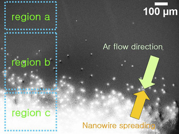
Figure 2 shows the SEM image of a sample adjacent to the Ar inlet within the annealing chamber. This single sample exhibited various regions reflecting different stages of SLS SiOx NW growth.
SEM image of a sample placed close to the Ar inlet inside the oven (low temperature/fast quench region). This sample has three distinct regions in terms of differentiable SLS NW growth stages.

Three regions were identified. In region “a”, Au–Si alloy nanoparticles reside on the surface, although NW nucleation had not yet occurred (the Au–Si particles are not visible in the magnification shown in Fig. 2). In region “b” the so-called “germinated” SiOx NWs could be observed. In region “c” fully formed SiOx NWs were clearly present.
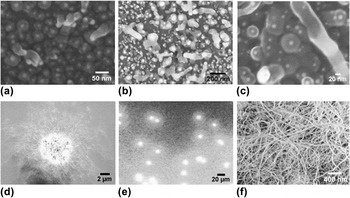
Figure 3(a) shows Au–Si alloy particles from the region “a” depicted in Fig. 2. Little, if any, NW nucleation is evident. The SEM images shown in Figs. 3(b) and 3(c) were acquired in the “b” region and clearly capture the initial formation of SiOx NWs from droplets wherein the amorphous Si NW can be seen emerging or “germinating” from the droplets. Flower-like structures were also observed [Figs. 3(d) and 3(e)] from the “c” region in which dense SLS NW nucleation was localized. SEM images from deeper within the “c” region show dense mats of NWs from the flower-like structures that had spread out and locally covered the substrate [Fig. 3(f)].
SEM images of SLS NWs at various stages of growth taken from the sample shown in Fig. 2. (a) Au–Si alloy particles from region “a”, (b) and (c) germination of NWs also from region “a”, (d) and (e) flower-like NW nucleation from region “b”, (f) normal morphology of NWs from region “c”.

The dense, entangled NW morphology of this latter feature is more consistent with SLS NW morphologies observed from regions of the substrate located at the center of the chamber. SLS NWs originating from the flower-like structures were substantially greater in length and density than more isolated SLS NWs nucleating nearby. On closer inspection, the flower-like NW clusters were seen to originate from pyramidal pits in the Si substrate (Fig. 4). The formation of thermally induced pyramidal etch pits in single crystalline Si (unrelated to SLS NW growth) has been observed previously. A thermal etching process results in formation of the pits by reaction of solid state oxide and silicon atoms along with preferential crystallographic facets.Reference Ueda and Yoshimura21–Reference Yazdi, Syvajarvi and Yakimova25 Regarding the specific formation mechanism of thermal etch pits, it has been reported that trace amounts of oxygen enhances the thermal etching process at high temperatureReference Reisman, Edwards and Smith23, Reference Reisman, Temple and Smith24 and that pits originate at substrate dislocation sites.Reference Yazdi, Syvajarvi and Yakimova25 The data in Figs. 2 and 3 imply preferential SLS NW growth at pyramidal thermal pit sites in the Si substrate.
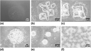
SEM images of NW synthesis steps via thermal pit-assisted growth, (a) formation of “embryos” on Si substrate, (b) thermal pit formation—the pyramidal pits are created by a thermal etching process, (c) initial NW growth between the pits, (d) coverage of pyramidal pit by SLS NWs, (e) NWs covering multiple pits, and (f) NWs coalescing from neighboring pyramidal pits to cover the substrate.

IV. EXPERIMENTAL OBSERVATION OF A NOVEL SLS SiOX NW GROWTH SEQUENCE
Figure 4 shows a detailed series of micrographs documenting this thermally quenched sequence of SLS SiOx NW growth steps at pyramidal pits in the Si substrate. Figure 4(a) shows the first step in thermal pit-assisted SLS NW growth from the boundary area between the regions “a” and “b” shown in Fig. 2—a circular region ∼10 μm in diameter of local volume discontinuity (swelling) developed in the Si wafer substrate. Regions of the substrate which experienced lower temperatures did not exhibit these features. The volume discontinuity is attributed to local oxidation of the Si substrate. Similar localized volume increases have long been observed during thermal oxidation processing of Si. Figure 4(b) shows the next step in this novel SLS NW growth mode—thermally induced formation of pits in the circular oxidation regions. These pits were pyramidal in shape with sidewalls comprising intersecting {111} planes in the (100) silicon wafer.Reference Reisman, Temple and Smith24, Reference Futagami and Hamazaki26 It was observed for multiple samples and experimental runs that the pyramidal pits in the Si substrate were formed before SLS NW growth. Figures 4(c) and 4(d) show NW nucleation and growth that occurred preferentially at the pyramidal pits. Figures 4(e) and 4(f) show the coalescence of SLS NWs from the pyramidal pit regions.
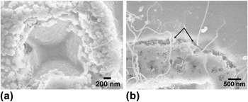
Figure 5 affords closer inspection of the pyramidal pit area at the onset of SLS NW nucleation. First, the Au–Si alloy droplet concentration is localized at the edge of the pyramidal pits [Fig. 5(a)]. Second, the silicon oxide growth front defining the circular region encompassing the pyramidal pit is clearly visible [black arrows in Fig. 5(b)]. The silicon oxide exhibits a granular or porous structure consistent with the local oxidation-induced volume change.
SEM images of (a) the center of a pit showing Au–Si alloy particles on the edge of the pit, and (b) the border of the pit area. In (b) the growth front separating the crack-oxidized region from the Si surface is clearly visible (black arrows).

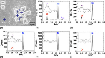
The material disposition associated with the regions in and around the pyramidal pits shown in Figs. 4 and 5 was investigated via SEM-EDS. Representative SEM-EDS spectra acquired in and around a cluster of pyramidal pits are shown in Fig. 6. Figure 6(a) shows the SEM image of the pit cluster and positions where EDS spectra were acquired. An EDS spectrum acquired from the bright region at the edge of the pits is shown in Fig. 6(b) and indicates the presence of Au, Si, and O, confirming the presence of Au–Si alloy droplets [Fig. 5(a)] and SiOx. The lower contrast region between the pits (but within the circular oxidized region) reveals smaller amounts of Au [Fig. 6(c)] and implies that Au–Si alloy droplets congregate preferentially at the pit edges (although the spectrum confirms the presence of oxidized Si). Away from the circular region confining the pits, EDS spectrum of the bare Si substrate does show smaller amounts of oxygen [Fig. 6(d)], which is attributed to the native oxide. Interestingly, EDS data from the very center of a pit [Fig. 6(e)] show no appreciable amounts of Au or O. Trace amounts of O are observed further up the pit walls, closer to the pit edge [Fig. 6(f)], where no Au was shown. Combined with the SEM image data of Figs. 3–5, the EDS data of Fig. 6 enabled the formulation of the SLS NW growth mechanism promoted by the pyramidal pits. An elaboration of this mechanism is provided in the following section.
SEM-EDS spectra at a thermal pit cluster. (a) SEM image of the pit cluster, (b) EDS spectrum at a high-contrast region near a pit edge (position 1), (c) EDS spectrum at a low-contrast region between pits (position 2), (d) EDS spectrum at the silicon substrate away from the pit cluster (position 3), (e) EDS spectrum at the center of a pyramidal pit (position 4), and (f) EDS spectrum at the sidewall of a pyramidal pit near the edge (position 5).

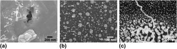
It is important to differentiate this newly observed thermal pit-assisted growth mode from previously reported SLS growth processes. In SLS NW growth, the Au–Si alloy droplet is generally observed at the bottom of the NW on the surface of the substrate. It has been previously observed that NWs can nucleate from alloy droplets inside pits on the silicon surface—pits that had been created by the inflow of the silicon to the alloy droplet.Reference Paulose, Varghese and Grimes11, Reference Lee, Rogers, Carpenter, Eisenbraun, Xue and Geer18, Reference Kim, An, Woo and Yoon20 This type of growth was also observed in this work. An example is shown in Fig. 7(a). Note that these types of pits (or voids) are irregular and do not exhibit the characteristic pyramidal morphology, which is described earlier.
SEM images of: (a) NW and pit created by the inflow of the silicon to the alloy droplet, (b) NWs directly grown from the substrate and nanoparticles, and (c) NW germination and growth.

SLS Si NW growth can also proceed without necessitating pit formation.Reference Wang, Chan, Xiao, Lin and Shiha27, Reference Elechiguerra, Manriquez and Yacaman28 Such a process was also observed in this work [Figs. 7(b) and 7(c)]. These conventional processes (growth modes) are typically used to explain the growth mechanism of SLS NWs. However, these growth modes are distinct from the sequence depicted in Figs. 3 and 4. Because of the spatial and temporal thermal gradients afforded by sample placement in the chamber and the rapid Ar gas flow, a spatially resolved “timeline” for this novel growth process was documented via SEM imaging at appropriate positions on the substrate.
In a detailed observation, the NWs start to grow at the edge of the thermally etched pits, not inside the pits, which is distinguished from previously reported research.Reference Paulose, Varghese and Grimes11, Reference Lee, Rogers, Carpenter, Eisenbraun, Xue and Geer18, Reference Kim, An, Woo and Yoon20
V. MECHANISTIC DESCRIPTION OF THERMAL PIT-ASSISTED SLS SiOX NW GROWTH
On the basis of the extensive SEM and SEM-EDS analysis (consistent with data shown in Figs. 3–6) of thermal pit-assisted SLS NW growth, it is concluded that a four-step sequence typifies this growth mode: (i) nucleation/growth of circular silicon oxide regions, (ii) thermally driven pyramidal pit formation, (iii) enhanced Au–Si alloy droplet formation at pyramidal pit edges, and (iv) onset of SLS NW growth from enhanced Au–Si alloy droplets.
The first step in the aforementioned sequence is consistent with previous observations of the decomposition and removal of SiO at high temperatures (1100 °C) from Si wafers, leaving nearly circular regions several microns in diameter.Reference Rubloff, Tromp, van Loenen, Balk and LeGoues29, Reference Tromp, Rubloff, Balk and LeGoues30 In this process, solid state SiO2 reacts with solid Si atoms to form volatile SiO groups. This reaction and the subsequent release of SiO are consistent with the circular regions shown in Figs. 4 and 6 and the porous microstructure within these regions seen in Fig. 5(b).
The oxidation kinetics in the circular regions are also consistent with pyramidal pit growth at high temperatures (>1000 °C). As noted above, Fig. 4(b) indicates that the thermally etched pyramidal pits are formed along {111} planes from the (100) silicon wafer in agreement with observations of other research groups. It should be noted that this reference reported a fiber-like SiO2 material at the periphery of Si wafer substrates after annealing for 30 min at 1100 °C. This observation is quantitatively and qualitatively distinct from the work reported here in that the author did not use a Au catalyst and the fiber-like material was only observed at the wafer periphery. Most importantly, the fiber-like material formation did not originate from nor was associated with thermal pit formation. It was more likely that this growth was related to oxide-assisted nanowire growth (OAG) [15–17].Reference Reisman, Edwards and Smith23, Reference Reisman, Temple and Smith24, Reference Futagami and Hamazaki26, Reference Suzuki31 Trace amounts of oxygen enhanced this thermal etching process at high temperaturesReference Reisman, Edwards and Smith23, Reference Reisman, Temple and Smith24 with pits originating at substrate dislocation sites.Reference Yazdi, Syvajarvi and Yakimova25 This supports our observation of pyramidal pit growth in the circular oxidized regions of the Si substrate [Figs. 4(a) and 4(b)]. The source of the oxygen is attributed to solid state SiO2,Reference Reisman, Edwards and Smith23 not gas phase oxygen from the chamber. Indeed, research has shown that pyramidal pit formation occurs preferentially under low oxygen partial pressure (below 3 × 10⁻⁵ atm) during annealing in Ar.Reference Suzuki31–Reference Suzuki33 Those researchers observed no pit formation at higher partial oxygen pressures. This is consistent with our experimental configuration. High-purity industrial grade Ar (99.999%) was utilized in our experiment with an oxygen filter loop. Assuming no other sources, the oxygen partial pressure in our system is ostensibly less than 10−6 atm based on the Ar gas purity. This is well below the upper limit of 3 × 10⁻⁵ atm noted in Refs. Reference Suzuki31–Reference Suzuki33 for preferential pit formation. It is not expected that other potential oxygen sources (e.g., quartz tube furnace, sample holder, vacuum excursions, native oxide on the Si wafer, etc.) impact the partial pressure.Reference Surdu-Boba, Sullivana, Saieda, Layberrya and Aflorib34, Reference Pan, Dai, Ma and Wang35
The formation of volatile SiO groups as a driving force for the pyramidal etch front is supported by the EDS spectrum in Fig. 6(e). No oxygen or Au is evident at the very center of the pit, whereas small trace amounts of oxygen (but no Au) are revealed on the pyramidal pit sidewall nearer the pit edge. The relatively high SiO partial pressure at the pit results in adsorption of SiO on Au nanoparticles near the pit edges. This has two primary results. First, Si saturation occurs in the Au–Si alloy droplets at the pit edges comparatively faster than in Au–Si alloy droplets formed on the planar Si wafer surface away from the pyramidal pits. Second, oxygen from the SiO species adsorbed on the Au nanoparticles is available to react with the Si substrate, thus driving the circular SiOx growth front and promoting additional pyramidal pits. As the pits cluster, their etch fronts converge, enhancing local concentration of Au–Si alloy droplets leading to a density of SLS NW nucleation sites. This speculation is wholly consistent with the observation of a relatively high density of Au–Si alloy nanoparticles adjacent to the thermally generated pits [Figs. 4(c) and 5(a)]. Also, Au–Si alloy droplets at the pit edges exhibited, on average, larger diameters as compared to alloy nanoparticles formed at the planar Si wafer surface away from the pits. As a natural consequence, SLS NWs nucleate and grow more rapidly from the Au–Si alloy droplets at the thermally generated pit edges as compared with Au–Si alloy droplets at the planar Si wafer surface. This speculation is strongly supported by SEM images shown in Figs. 4(e) and 4(f).
It is essential to differentiate the mechanism described above with so-called OAG. In OAG, thermal evaporation or laser ablation is used to evaporate SiO or SiO2–Si. The resulting SiO vapor decomposes into Si and SiO2 resulting in a NW-like growth front as described in the literature.Reference Zhang, Lifshitz and Lee15–Reference Zhang, Chu, Cheung, Wang and Lee17 Isolated NW growth reported in Ref. Reference Reisman, Temple and Smith24 was related to the OAG growth mode as the Si sample was annealed at 1000 °C for 48 h without a metal catalyst.
In our experiment, the volatile SiO results specifically from pit formation. NW growth is catalyzed by Au nanoparticles at the pit edges, which serve as SiO adsorption sites. The Au nanoparticles simultaneously promote Si NW formation through the SLS process and maintain local SiOx growth, further promoting pit formation.
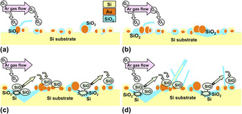
This process is described schematically in Fig. 8. Figure 8(a) depicts the surface of the Au-coated Si wafer following thermally induced dewetting of the Au, which results in the formation of Au–Si alloy droplets on the substrate. At selected regions, larger Au–Si alloy droplets are formed via ripening effects. Dangling bonds associated with substrate silicon atoms promote local oxidation (from both low partial pressure gas phase oxygen and solid oxide sources) and is shown in Fig. 8(a). Continued oxidation and SiO volatilization lead to the formation of circular SiOx regions [Fig. 8(b)] and, eventually, to pyramidal pit etching [Fig. 8(c)]. Continued pit etching results in an increase in volatile SiO concentration which promotes relatively faster Si saturation of Au–Si alloy droplets [Fig. 8(d)]. This promotes more rapid SLS NW growth compared with nucleation on the planar Si substrate. If pyramidal pit density is sufficient, a mat-like morphology of thermal pit-assisted NWs coalesces and forms a dense network of NWs.
Schematic illustration of the mechanism of thermal pit-assisted growth mode, (a) oxidation of germinated silicon, (b) oxidation of silicon substrate, (c) reaction between solid state SiO2 and Si, resulting in volatile SiO and etched pit. Volatile SiO groups can adsorb to Au–Si alloy droplets at the pit edge, and (d) NW growth from accumulated Au–Si alloy droplets.

VI. CONCLUSION
The fundamental kinetics and growth mechanisms of SLS SiOx NWs were investigated. A previously unreported SLS growth process was observed. For that growth process, it is concluded that the high temperature formation of pyramidal etch pits in the Si wafer substrate resulted in local enhancement of Au–Si alloy droplet formation through the production of volatile SiO groups from a solid state SiO2–Si reaction. Saturation of the Au–Si alloy droplets at the pyramidal pit edges due to adsorption of SiO groups occurred more rapidly than Si saturation of Au–Si alloy droplets at the planar Si wafer surface. This resulted in relatively faster SLS NW nucleation and growth. This growth mode is termed as “thermal pit-assisted growth.”
ACKNOWLEDGMENTS
The authors acknowledge the SRC (Semiconductor Research Corporation)/DARPA (Defense Advanced Research Projects Agency) Focus Center Research Program and the New York State Office of Science, Technology and Research for their support of this work.