Introduction
Single-walled carbon nanotubes (SWNTs) have been explored by researchers from various fields because of the unique 1D structure and exceptional electrical properties, namely high carrier mobility, mechanical and thermal robustness.[Reference Jorio, Dresselhaus and Dresselhaus1] However, the interface engineering of SWNTs has not been fully understood when they are incorporated in 3D devices. Here, we discuss the application of SWNT films in Lead halide perovskite solar cells (PSCs) which have emerged recently. PCSs have attracted much attention around the world as the efficient alternative energy harvesting devices.[Reference Green, Ho-Baillie and Snaith2] Miyasaka and colleagues demonstrated the first application of perovskite materials in replacement of organic dyes.[Reference Kojima, Teshima, Shirai and Miyasaka3] The research gained momentum when Park and colleagues resolved the instability issue of the perovskite materials in the electrolyte by developing a solid-state submicron perovskite layer.[Reference Kim, Lee, Im, Lee, Moehl, Marchioro, Moon, Humphry-Baker, Yum, Moser, Grätzel and Park4] Now, the certified power conversion efficiencies (PCEs) exceed 22%.[Reference Yang, Park, Jung, Jeon, Kim, Lee, Shin, Seo, Kim, Noh and Seok5] Despite the high PCEs, the low stability and high fabrication-cost of PSCs still remain as unresolved problems. Lately, SWNT electrodes have been used as an electrode in PSCs to solve the aforementioned problems by replacing expensive metal electrodes.[Reference Jeon, Chiba, Delacou, Guo, Kaskela, Reynaud, Kauppinen, Maruyama and Matsuo6–Reference Aitola, Sveinbjörnsson, Correa-Baena, Kaskela, Abate, Tian, Johansson, Grätzel, Kauppinen, Hagfeldt and Boschloo9] However, the devices still rely on hole-transporting materials (HTMs), which are also expensive and impose stability limitation.[Reference Chen and Yang10, Reference Wu, Song and Sun11]
In this work, SWNT-based PSCs where SWNTs are replacing the metal electrodes were fabricated without the use of HTMs. There have been numerous reports claiming that thick SWNTs can function as the HTM, contradicting high purity semiconducting SWNTs.[Reference Jeon, Matsuo and Maruyama12, Reference Schulz, Dowgiallo, Yang, Zhu, Blackburn and Berry13] It was our prognosis that we could achieve high-performance PSCs without the use of HTMs by employing SWNT as the top electrode. Lead halide perovskite was deposited via the one-step adduct method,[Reference Ahn, Son, Jang, Kang, Choi and Park14] followed by SWNTs lamination. The metal- and HTM-free PSCs produced a PCE of 10.0%. Upon drop-casting poly(methyl methacrylate) (PMMA) on top of SWNTs, the PCE increased to 11.8%. Moreover, the hysteresis was reduced and the stability of the devices was improved significantly. According to our analyses, the application of PMMA-densified SWNT film increased every photovoltaic parameter, namely short-circuit current (J SC), open-circuit voltage (V OC), and fill factor (FF). This was due to the densification of SWNTs by PMMA, which increased the conductivity of SWNT films. PMMA also functioned as an effective encapsulation, improving the stability.
Methodology
Synthesis of SWNT films
Randomly oriented SWNTs are synthesized by the aerosol chemical vapor deposition (CVD) method.[Reference Nasibulin, Kaskela, Mustonen, Anisimov, Ruiz, Kivistö, Rackauskas, Timmermans, Pudas, Aitchison, Kauppinen, Brown, Okhotnikov and Kauppinen15] The aerosol CVD method produces highly pure and long SWNT networks. It was carried out in a scaled-up reaction tube with a diameter of approximately 150 mm. The catalyst precursor was vaporized in ambient temperature CO atmosphere through a ferrocene powder-filled cartridge. A controlled amount of CO2 was added to the carbon source (CO) in order to achieve stable growth of SWNTs. SWNTs were collected by filtering the flow through a nitrocellulose film (Millipore Corp., USA; HAWP, 0.45 µm pore diameter). The collected SWNT networks were transferred to a variety of substrates through the dry press-transfer process.
Solar cell fabrication
Fluorine-doped tin oxide (FTO) (Peccell Technologies, ~10 Ω/cm2) were used after cleaning in isopropanol, acetone, and distilled water using an ultrasonic bath, followed by annealing at 500 °C. A compact TiO2 layer on the FTO-coated glass substrates was prepared by spin-coating of titanium diisopropoxide bis(acetylacetonate) solution (0.15 M, in ethanol) at 5000 rpm for 30 s, dried at 125 °C for 5 min, then repeated twice with 0.3 M of titanium diisopropoxide bis(acetylacetonate) solution, finally annealed at 500 °C for 15 min.
The MAPbI3 perovskite layers were fabricated according to Ahn et al.[Reference Ahn, Son, Jang, Kang, Choi and Park14] A 1 : 1 : 1 molar ratio mixture of PbI2 (TCI), MAI (TCI),[Reference Kim, Lee, Im, Lee, Moehl, Marchioro, Moon, Humphry-Baker, Yum, Moser, Grätzel and Park4] and dimethyl sulfoxide (DMSO) (Sigma-Aldrich) was dissolved in dimethylformamide (DMF) (Sigma-Aldrich) at 50 wt% without heating. The fully dissolved solution was spin coated onto TiO2 layer at 4000 rpm for 30 s, with a dropping of 0.1 mL diethyl ether 7.5 s after starting the spin-coating process. The transparent green film, so-called CH3NH3I•PbI2•DMSO adduct film, changed to a dark brown color by heating at 100 °C for 20 min.
SWNT film was applied directly onto the perovskite film using a pair of tweezers. A drop of chlorobenzene was applied to improve the contact between the perovskite film and the SWNT film. The SWNT film was ca. 200 nm thick. Three droplets of PMMA, which was prepared by dissolving 1 mg of PMMA (Average Mw ~996,000 by GPC crystalline, Aldrich) in 100 mg of anisole (Aldrich), were applied to densify the SWNT film. This was followed by annealing at 80 °C for the 30 s. The thickness of the SWNT film reduced to ca. 100 nm due to densification.
Characterizations
J − V characteristics were measured by software-controlled source meter (Keithley 2400) in both the dark and under illumination of 1 sun AM 1.5 G simulated sunlight (100 mW/cm2) using a solar simulator (EMS-35AAA, Ushio Spax Inc.) with Ushio Xe short ark lamp 500, calibrated by a silicon diode (BS-520BK, Bunkokeiki). Shimadzu UV-3150 was used for the UV-vis-NIR (near infra-red) measurement. Integrated photoconversion efficiency (IPCE) system consisted of an MLS-1510 monochromator to scan the UV-vis spectrum. Valence band information and Fermi levels were measured by Riken Keiki photoelectron yield spectroscopy (PYS) PYS-A AC-2 and Kelvin probe S spectroscopy in the air (ESA), respectively. They were calibrated by Au before the measurement. Solartron SI1287 Electrochemical Interface and Solartron 1255B Frequency Response Analyzer were used for the Impedance Measurement. Photoluminescence (PL) was measured using JASCO FP6500 spectrophotometer; at room temperature (298 K) in a 1 × 1 cm glass substrate. An excitation wavelength of 500 nm was used.
Results and discussion
Recently, SWNT has been regarded as promising electrodes for in PSCs since earth-abundance, easy synthesis, and direct roll-to-roll expected processability.[Reference Jeon, Seo, Sato, Delacou, Anisimov, Suenaga, Kauppinen, Maruyama and Matsuo16] High quality and directly transferrable SWNT films have been developed by Kauppinen and colleagues.[Reference Nasibulin, Kaskela, Mustonen, Anisimov, Ruiz, Kivistö, Rackauskas, Timmermans, Pudas, Aitchison, Kauppinen, Brown, Okhotnikov and Kauppinen15] The randomly oriented SWNT networks with high purity were synthesized using the aerosol CVD. Floating catalyst aerosol CVD was performed in a tube with a diameter of 150 mm. As the process did not require the dispersion step, the resulting SWNT network contained long SWNTs. The SWNT films were easily peeled off from a nitrocellulose film and transferred onto the perovskite layer of PSCs (glass/FTO/TiO2/CH3NH3PbI3) using a pair of tweezers.[Reference Jeon, Delacou, Kaskela, Kauppinen, Maruyama and Matsuo17] A few drops of chlorobenzene were added to enhance the interface adhesion between the SWNT film and the perovskite layer. In the case of PMMA-applied CNT-laminated PSCs, we applied the solution of PMMA onto the SWNT film instead of chlorobenze.
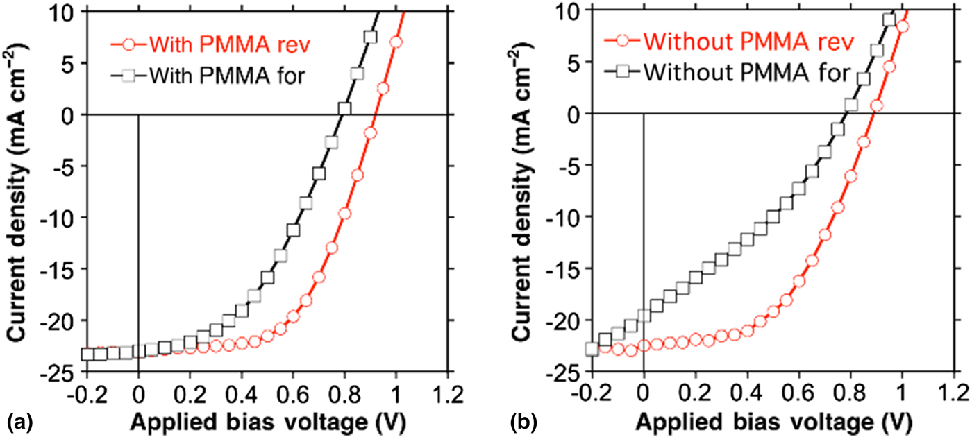
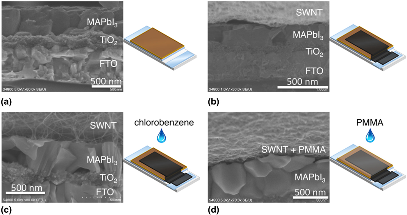
According to the photovoltaic measurements in Fig. 1, SWNT-applied metal-free PSCs produced a PCE of 10.0% even in the absence of HTMs. This was due to the fact that both the perovskite layer (CH3NH3PbI3) and SWNTs can partially function as the HTM.[Reference Jeon, Matsuo and Maruyama12, Reference Schulz, Dowgiallo, Yang, Zhu, Blackburn and Berry13, Reference Laban and Etgar18] A recent study by Blackburn and colleagues proved that an interface dipole is formed through the selective charge transfer from methylammonium ion to SWNT, leading to the band alignment.[Reference Jeon, Cui, Chiba, Anisimov, Nasibulin, Kauppinen, Maruyama and Matsuo19] A simple over-coating of SWNT film with a solution of PMMA increased the PCE by approximately 2%. This improvement was due to the increases in all three photovoltaic parameters, V OC, J SC, and FF (Table I). From the photovoltaic data and current-voltage (J − V) curves, we observed that the difference between forward and reverse J − V curves was much reduced (Fig. 1). This indicates that the application of PMMA reduced hysteresis. Cross-sectional scanning electron microscopy (SEM) images in Fig. 2 show the interface between SWNT film and the perovskite layer. Before the application of chlorobenzene, some parts of the SWNT film do not make full contact with the perovskite layer [Fig. 2(b)]. After the application of chlorobenzene, magnified SEM images show that the SWNT film makes full contact with the perovskite layer. From Fig. 2(d), we can see that the addition of PMMA densifies the SWNTs. Polymeric gel-like PMMA seems to have percolated into the network of SWNTs, filling the air gaps and reducing the thickness of the SWNT film. From the J − V curves in Fig. 1(a), we can see that the application of PMMA reduced hysteresis. The reduction in hysteresis can also be explained by the decreased trapped charge in the SWNT film. According to the study conducted by Choi and colleagues,[Reference Ahn, Kwak, Jang, Yoon, Lee, Lee, Pikhitsa, Byun and Choi20] hysteresis is caused by trapped charge at the interface of the perovskite layer and can be reduced by effective charge extraction. Our hypothesis is that the densification of SWNTs by PMMA can extract trapped charge more effectively through the better adhesion between SWNTs and perovskite layer [seen by arrows in Figs. 2(c) and 2(d)].
J − V curves of (a) SWNT film-laminated PSC with PMMA and (b) the same SWNT film-laminated PSC without PMMA under AM 1.5 G one sun illumination (100 mW/cm2). (The aperture mask area was 0.1 cm2 with a scan rate of 200 ms from 1.2 to −0.2 V. Reverse bias was measured first followed by forward bias).

Cross-sectional SEM pictures of (a) a PSC without HTM and metal electrode, (b) a SWNT film-laminated PSC before chlorobenzene addition, (c) a SWNT film-laminated PSC after chlorobenzene addition, and (d) a SWNT film-laminated PSC after PMMA addition, the white arrows showed the effect of chlorobenzene and PMMA addition of filling gaps and increasing the adhesion between SWNT and perovskite layer.

Photovoltaic data of SWNT-applied PSCs with and without PMMA under one sun (AM1.5 G illumination, 100 mW/cm2).

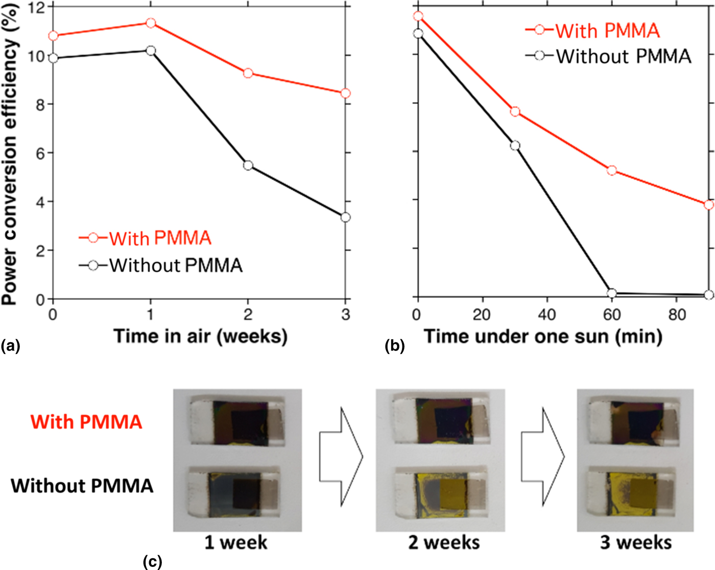
The role of PMMA was not limited to densifying the SWNT network, it also encapsulated the devices against atmospheric moisture effectively. Although SWNT has the hydrophobic nature, our water vapor transmittance rate (WVTR) measurements show that the SWNT film alone was not enough to block moisture and that the application of PMMA greatly improved the barrier ability of SWNTs (Fig. S1). Indeed, the stability tests in ambient conditions and under 1 sun showed that the PMMA applied-devices were much more stable compared with the PSCs without PMMA as displayed in Fig. 3. In particular, the stability test under one sun indicates degradation induced by trapped charges seen in Fig. 3(b). The fact that the PMMA-applied devices lasted longer indicates that PMMA-densified SWNT film reduced trapped charges, which triggers light-induced degradation.
Stability test results of SWNT film-laminated PSCs with PMMA and without PMMA (a) in ambience (25 °C, 13%) over time, and (b) under illumination of one sun. (c) Degradation pictures of SWNT film-laminated PCSs with and without PMMA in ambience over time.

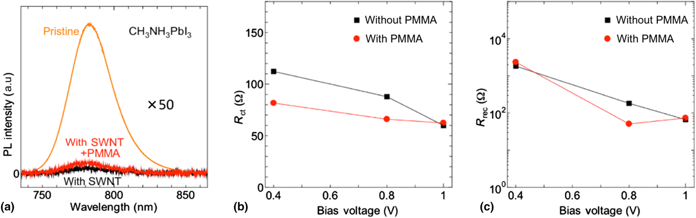
The improvement in J SC and FF were investigated using various analyses. The UV-vis transmittance spectra in Fig. S2(b) showed no difference. However, the IPCE spectra in Fig. S2(a) shows that there is an increase of the integrated J SC of ca. 2.78 mA/cm2, indicating a better contact between perovskite and SWNT with PMMA. This reveals that the PMMA had no optical effect because the sunlight was shone from the FTO side, and the increase in J SC was not influenced by absorption but solely by the improved contact.[Reference Gan, Lv, Zhu, Ma, Wang, Zhang, Huang, Zhu, Ren, Terrones and Kang21] To investigate charge extraction after the PMMA application, PL and impedance measurement were conducted. From the PL measurement data in Fig. 4(a), the suppression of the lead halide perovskite film PL spectrum is patently observable after the deposition of SWNT compared with PMMA-densified SWNTs. While this confirms efficient charge extraction, the difference in charge extraction after the PMMA application was difficult to observe even after magnification of the intensity by 50-fold. In general, a Nyquist plot is based on an equivalent circuit of PSCs, consisting of a series resistance (R s, starting point of the first semicircle of the Nyquist plot), electron transport resistance at the counter electrode (R ct, first semi-circle in the Nyquist plot), and recombination resistance (R rec second semicircle in the Nyquist plot) as shown in Fig. S3.[Reference Yue, Chen, Wang, Zhang, Hu and Zhu22] Accurate comparisons of R ce and R rec can be made by reading impedance graphs over different potentials [Figs. 4(b) and 4(c)]. It is well known that R s and R ct are parts of the total series resistance of PSCs.[Reference Li, Boix, Xing, Fu, Kulkarni, Batabyal, Xu, Cao, Sum, Mathews and Wong23] Looking at the starting position of the curves in the Nyquist plot in Fig. S3, PMMA-applied PSCs have a similar R s. However, PMMA-applied PSCs showed a lower R ct compared with the devices without the application of PMMA, with no significant change in R rec. This indicates that it was the densification of SWNT electrode by PMMA that led to more efficient charge extraction with reduced hysteresis and increased FF. Because the increase in both J SC and FF can be caused by a doping effect of PMMA on SWNT, as previously been reported by several groups,[Reference Pirkle, Chan, Venugopal, Hinojos, Magnuson, McDonnell, Colombo, Vogel, Ruoff and Wallace24–Reference Im, Lee, Lee, Park and Park30] we used four-probe measurement PYS to confirm the effect. For the four-probe measurement, we pasted indium at the four corners of a pristine SWNT film and then spin-coated the film with PMMA (Fig. S4). There was a sheet resistance change before and after the PMMA deposition on a pristine SWNT film. We observed a decrease in sheet resistance by approximately 6 Ω/cm. According to the PYS measurement result in Fig. S5, SWNT film has a Fermi level of around 5.0 eV. After PMMA was applied to the SWNT film, it became impossible to detect the Fermi level. This was due to the PMMA coverage at the surface insulating electron transfer, making the Fermi level undetectable by PYS. We carried out vis-NIR absorption spectroscopy on SWNT films with and without PMMA. We found that the Van Hove peaks get weakened upon PMMA application, followed by thermal annealing (Fig. S6). This indicates that there might be a possible doping effect of PMMA on SWNTs, yet it is not conclusive at this stage.
(a) Photoluminescence spectra of a CH3NH3PbI3 film, a SWNT film laminated on the CH3NH3PbI3 film, and a PMMA-applied SWNT film laminated on the CH3NH3PbI3 film (intensity enhanced by 50-fold). (b, c). Impedance charge transfer measurements and recombination measurements derived from Nyquist plots of SWNT film-laminated PSCs with and without PMMA can be seen in Fig. S3.

Conclusion
In conclusion, we demonstrated decent performance SWNT-based PSCs without expensive metal electrodes and HTMs. By overcoating with PMMA, the SWNT film was densified which led to the PCE increase, reduction in hysteresis, and stability improvement in the air. We are confident that the demonstration of metal- and HTM-free PSCs and the discovery of SWNT densification by PMMA will accelerate carbon-based solar cell research and commercialization.
Supplementary material
The supplementary material for this article can be found at https://doi.org/10.1557/mrc.2018.142
Acknowledgments
We gratefully acknowledge the Research and Education Consortium for Innovation of Advanced Integrated Science by Japan Science and Technology (JST) and Japan Society for the Promotion of Science (JSPS) KAKENHI Grant Numbers (JP25107002, JP15H05760, and 17H06609), the CREST project, NSFC under the Japan-China Scientific Cooperation Program and IRENA Project by JST-EC DG RTD, Strategic International Collaborative Research Program, SICORP. Part of this work is based on results obtained from a project commissioned by the New Energy and Industrial Technology Development Organization (NEDO). N.-G.P. acknowledges financial support from the National Research Foundation of Korea (NRF) grant funded by the Ministry of Science, ICT & Future Planning (MSIP) of Korea under contract No. NRF-2012M3A6A7054861 (Global Frontier R&D Program on Centre for Multiscale Energy System).