Introduction
Purpose and application
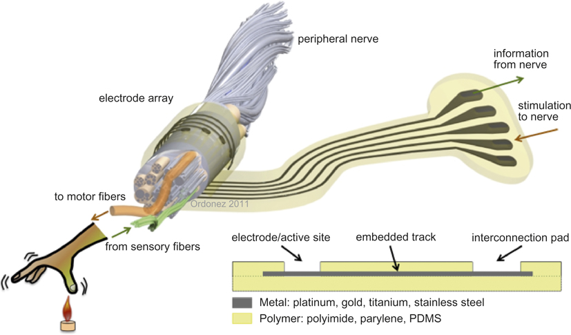
A microelectrode array is, in a broad sense, a very thin piece of plastic carrying embedded metallic structures, which is implanted into the human body to interact with the nervous system (Figure 1). We will take a short digression into the applications for such devices in order to understand the need for them. The signals in the body traveling from the brain to the muscles to elicit muscle motion are electrical, as are signals going from the sensory organs to the brain (e.g., hearing, vision, and sensing). The nervous system transports these signals. If a nerve is injured and the communication between the brain and the periphery is disrupted, as in the case of spinal cord injury, it is possible to use a device to either record this information from the nervous system or to restore the function that the brain cannot control. The nerves that need to be controlled must still be present. In the case of nerve degeneration or peripheral nerve injury, electrical stimulation cannot be used.Reference Kern, Hofer, Mödlin, Forstner, Raschka-Högler, Mayr and Stöhr1 Devices such as bladder control stimulatorsReference Brindley2 for patients with incontinence, leg stimulation for cycling,Reference Donaldson3 and drop-foot stimulatorsReference Taylor, Burridge, Dunkerley, Wood, Norton and Singleton4–Reference Burridge, Sinkjaer, Larsen, Haugland and Pickering6 for stroke patients are examples of successful technical intervention in the periphery of the body. More complex devices such as cochlear implants to restore hearingReference Clark7 are a further example of the implementation of devices to restore lost body functions. Neural prostheses to restore visionReference Stieglitz8–Reference Weiland12 are the most complex example of miniaturized implants but are still in the experimental stage, though some of them have already received approval as medical devices.Reference Humayun, Dorn, Ahuja, Caspi, Filley, Dagnelie, Salzmann, Santos, Duncan and daCruz13, Reference Argus14 Electrical stimulation of the vagalReference Albert, Cook, Prato and Thomas15–Reference Amar18 nerve or deep structures of the brainReference Groves and Brown16 has been applied to treat the symptoms of Parkinson’s disease (tremor, akinesia, dyskinesia), to suppress epileptic seizures, and to treat severe psychiatric disorders such as depression and obsessive-compulsive disorder.Reference Stieglitz19 It is also possible to read out the electrical signals of the brainReference Patil and Turner20 and bodyReference Toledo, Leija, Munoz, Vera and Ramirez21 and use them as control signals for assistive devices in rehabilitation, for control of artificial limbsReference Donoghue22 or communication (e.g., maneuvering a mouse pointer on computer displays for interacting with a word processor). These devices are known as brain-machine interfaces,Reference Stieglitz, Rubehn, Henle, Kisban, Herwik, Ruther and Schuettler23 and they target immobile patients who have suffered from severe brain stroke, a disease such as amyotrophic lateral sclerosis (Lou Gehrig’s disease), or patients who have lost a limb through disease or accident.
Conceptual sketch of a polymer-based microelectrode array for interfacing with the nervous system. Embedded microwires transport signals to or from the nerve. Sensory signals can be read, and motor fibers can be stimulated for motor movement. PDMS, poly(dimethylsiloxane).

All the disorders mentioned are different in cause and nature, but the basic approach to restore normal function starts by connecting the involved nerves—or in some cases individual neurons—to a device.Reference Zhou and Greenbaum24, Reference Zhou and Greenbaum25 Electrodes play a crucial role in interfacing with the biological environment at one end and with the implanted electronics providing the stimuli or recording the electrical signals at the other end.
In most of today’s applications, it is necessary to stimulate or record from multiple neurons either at the brain or within a nerve. A high spatial resolution is important, as this defines how precise and reproducible a recording or stimulation from a specific neuron or from a bundle of neurons will be. The higher the number of contacts, the better the resolution of the device. This leads to the use of multiple channels in a single device: an electrode array.
Requirements
An implanted electrode array acts as a bidirectional interface in direct contact with the nerve and has to fulfill various requirements. First of all, all the materials exposed to the body have to be biocompatible and biostable,Reference Hassler, Boretius and Stieglitz26 meaning the materials should not cause a harmful reaction in the biological environment. On the other hand, they should not be rejected or disintegrated by the body’s immunological system. Furthermore, a mechanical load on the nerves and surrounding tissue will also trigger a protective reaction to counteract the load.Reference Williams27 A persistent load might lead to non-reversible deterioration of the tissue, defeating the intent of the device.Reference Polikov, Tresco and Reichert28 The device therefore has to fulfill physical or structural biocompatibility. Beyond chemical and biological inertness, the metallic structures carrying out the stimulation have to be electrochemically stable over a wide range of electrical loading to deliver enough charge through the contact sites to trigger a biological response (an action potential) in the nerves without inducing irreversible electrical corrosion reactions.Reference Robblee, Cogan, Twardach, Rose, Jones and Kimball29, Reference Robblee and Rose30 Metals that have been widely implemented in electrode arrays are noble metals such as platinum and gold, medical-grade stainless steel, platinum-iridium alloy, and iridium oxide.Reference Robblee and Rose30–Reference Henle, Meier, Schuettler, Boretius and Stieglitz46
Microelectrode arrays can be roughly separated into two types: flexible and stiff. The flexible devices can be separated again into two types: first those fabricated with “common” machining methods such as milling, drilling, or (laser) cutting, and second those fabricated with micromachining processes such as photolithography and plasma deposition of materials. The advantages of each approach will be discussed in the following section.
Fabrication approaches and material choice
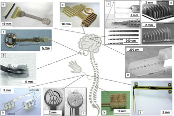
The specifications of an electrode array, such as size, shape, number of electrodes, electrical capabilities of contacts, thickness, and degree of stiffness (or flexibility), have to be chosen according to the application. For example, cuff electrodesReference Naples, Mortimer, Scheiner and Sweeney47–Reference Polasek, Hoyen, Keith and Tyler50 are rolled around nerves. Their most common application is in the peripheral nervous system (PNS), but cuffs have also been used to interface with the optical nerveReference Delbeke, Wanet-Defalque, Gerard, Troosters and Michaux51–Reference Veraart, Raftopoulos, Mortimer, Delbeke, Pins, Michaux, Vanlierde, Parrini and Wanet-Defalque53 (central nervous system [CNS]). Electrodes for hearing implants have the shape of a worm rolled into a spiral and are inserted into the cochlea.Reference Clark7 Retinal implants for partial restoration of vision are planarReference Stieglitz8, Reference Weiland12, Reference Suaning, Schuettler, Ordonez and Lovell35, Reference Weiland54 but have to adapt to the curvature of the back of the eye in order to provide intimate contact between the array and the tissue. A similar requirement is set for large brain arrays, which have to adapt globally to the spherical shape, but also to the irregularities on the surface of the brain.Reference Rubehn, Bosman, Oostenveld, Fries and Stieglitz44 Even though polymers are the material of choice considering their better mechanical compatibility with biological tissue, they do not provide the required stiffness to penetrate into neural tissue (e.g., the brain). For this purpose, stiff silicon-based probesReference Stieglitz, Rubehn, Henle, Kisban, Herwik, Ruther and Schuettler23, Reference Leuthardt, Schalk, Wolpaw, Ojemann and Moran55–Reference Warwick, Gasson, Hutt, Goodhew, Kyberd, Andrews, Teddy and Shad61 have been introduced. However, only one group is working on the transfer of these devices into clinical applications for cortical implantation in humans,Reference Hochberg, Serruya, Friehs, Mukand, Saleh and Caplan62 and except for some fundamental studies,Reference Warwick, Gasson, Hutt, Goodhew, Kyberd, Andrews, Teddy and Shad61 no silicon microprobes have been used in the PNS. Neural prosthetic devices typically implement flexible, polymer-based devices (Figure 2).
Overview of microelectrode arrays implemented in different sections of the nervous system. The central nervous system can be interfaced by (a–b) superficial arrays,Reference Rubehn, Bosman, Oostenveld, Fries and Stieglitz44, Reference Oh, Gilad, Ghosh, Schuettler and Holder66 (c–e) penetrating shafts or shaft arrays,Reference Navarro, Calvet, Rodríguez, Stieglitz, Blau, Buti, Valderrama and Meyer81, Reference Stieglitz102 or in the case of the eye, by planar electrodes (f–g).Reference Stieglitz8, Reference Rodger, Fong and Li42 The peripheral nerves can be interfaced by (h) cuff,Reference Schuettler, Gross, Staiger, Katzenberg and Stieglitz133 (i) sieve,Reference Navarro, Calvet, Rodríguez, Stieglitz, Blau, Buti, Valderrama and Meyer81 or (j) intrafascicularReference Hassler, Boretius and Stieglitz26 electrodes. (k) Book electrodesReference Schuettler, Vanhoestenberghe, Saeidi, Liu, Evans, Colinge, Demosthenous and Donaldson134 are implanted into the spinal cord.

Silicone-based devices
Devices that have made their way into clinical applications in medical prostheses (cochlear implants, cardiac pacemakers, bladder control) use 5–25-μm-thick metal foils milled or punched out of bulk material, embedded in thick (40–500 μm) bulk silicone rubber (poly(dimethylsiloxane) [PDMS]), which confines and insulates the individual metallic contacts.Reference Love63 The electrical leads reported so far consist of wires brazed or welded to the back of the stimulating electrode contact. The resolution of precision machining methods has limited the integration density of contacts, keeping the devices simple with only a few contacts. Schuettler et al. presented an interesting manufacturing process using laser structuring of metal foil,Reference Schuettler, Stiess, King and Suaning34 based on foundations laid by MortimerReference Mortimer41 and co-workers in the early 1990s. It provides a fabrication process for planar and flexible electrode arrays, which was varied, adapted, and refined to meet specific demands.Reference Robblee and Rose30–Reference Schuettler, Schroeer, Ordonez and Stieglitz33, Reference Suaning, Schuettler, Ordonez and Lovell35 Electrodes for stimulating the retina, peripheral nerve cuff electrodes, and devices incorporating microfluidic channels have been fabricated and tested since then, and densities of around 4.5 electrode sites per mm2 have been reported in a multilayer device.Reference Suaning, Schuettler, Ordonez and Lovell35
The materials processed by this method are limited to traditional implant materials such as medical grade silicone rubber and metal foil. The selection of the metal foil strongly depends on the individual application. For electrical stimulation purposes, platinum or platinum-iridium alloys are selected because of their advantageous electrochemical charge injection capacities.Reference Cogan64 In the case of sole electrical recording of neural signals or if quite large electrode sizes are acceptable, stainless steel (316 L) or MP35N (a nickel-cobalt alloy) is preferred, as they provide excellent corrosion resistance at moderate prices.Reference Henle, Meier, Schuettler, Boretius and Stieglitz46 Laser machining is tremendously flexible, and the achievable feature sizes are not dictated by the metal type but rather by the used laser technology and equipment. The thickness of metal foil that is commonly used lies between 5 μm and 25 μm. However, the most common choice of 12.5 μm is set by the tradeoff between ease of machinability and mechanical stability during fabrication. The mechanical properties (flexibility and spring behavior) of the microelectrode array should be dominated by the PDMS, which favors the use of thinner foils. On the other hand, handling the metal foil in fabrication is impractical for 5 μm foils and thinner, as they easily bend and crumple, decreasing the production yield.
Beyond this, the biocompatibility of these devices was successfully proven with respect to toxic effects on cell cultures as well as general bioacceptance in chronic animal studies.Reference Green, Ordonez, Schuettler, Poole-Warren, Lovell and Suaning36, Reference Henle, Raab, Cordeiro, Doostkam, Schulze-Bonhage, Stieglitz and Rickert39 Furthermore, neural signals have been recorded from the surface of the brain,Reference Gierthmuehlen, Ball, Wang, Henle, Raab, Stieglitz and Kaminsky65, Reference Oh, Gilad, Ghosh, Schuettler and Holder66 and stimulation of the retina was performed with use of such laser-machined arrays.Reference Tsai, Morley, Suaning and Lovell67
Silicon
Fabrication techniques for microelectromechanical systems have extended microelectrode fabrication possibilities to the microscopic world. Physical vapor deposition of metals on structures defined by photolithography and reactive ion etching reach feature sizes of only a couple of micrometers, allowing not only much higher contact integration densities than in PDMS-based methods, but also reaching the required spatial resolution of neural networks.Reference Stieglitz, Schuettler and Rubehn68 This has led to a broad development of silicon-based probes,Reference Stieglitz, Rubehn, Henle, Kisban, Herwik, Ruther and Schuettler23, Reference Leuthardt, Schalk, Wolpaw, Ojemann and Moran55–Reference Warwick, Gasson, Hutt, Goodhew, Kyberd, Andrews, Teddy and Shad61, Reference Richardson, Miller and Reichert69, Reference Wise, Angell and Starr70 which provide thinness and stiffness. Neuroscience benefits from these probes,Reference Maynard, Nordhausen and Normann71, Reference Rousche and Normann72 which allow for accessibility of deeper brain regions with high resolution. However, besides a limited number of clinical studies, no application in a neural prosthetic device has been reported yet.
Insertion of a stiff material triggers a biological reaction in the neural tissue to protect the neurons. Electrically silent nervous tissue cells, known as glial cells, grow at the invasion site, leading to formation of a glial scar. The large mismatch in elastic propertiesReference Polikov, Tresco and Reichert28, Reference Lefurge, Goodall, Horch, Stensaas and Schoenberg73 becomes an issue during extended use because of the natural movement of the brain during respiration and heartbeat.Reference Gilletti and Muthuswamy74 Furthermore, silicon-based probes suffer from degradation due to dissolution of silicon and silicon dioxide in saline.Reference Shelby75, Reference Alexander, Heston and Iler76 Special coatings are required to avoid such reactions.Reference Sweitzer77 The more complex the material combinations become, the more complicated it is to fabricate a stable device, since not all materials are biocompatible, and electrochemistry on dissimilar metal combinations is likely to occur. As mentioned before, protruding silicon probes have been tested in the PNS but have not found an application in commercially available rehabilitation or prosthetic devices. Some groups and companies are working on silicon-based devices (e.g., Neuronexus or Retina Implant AG) for long-term application in the CNS. There is a strong focus on fabricating reliable inorganic and polymeric coatings (e.g., DLC, Al2O3, or parylene) to insulate the delicate materials and overcome the mentioned issues.
Polyimide/parylene
The use of polymersReference Hassler, Boretius and Stieglitz26 such as polyimide and parylene has extended the field of microelectrode arrays to flexible devices.Reference Stieglitz8, Reference Kelly, Shire, Chen, Doyle, Gingerich, Drohan, Theogarajan, Cogan, Wyatt and Rizzo9, Reference Weiland12, Reference Humayun, Dorn, Ahuja, Caspi, Filley, Dagnelie, Salzmann, Santos, Duncan and daCruz13, Reference Amar18, Reference Zhou and Greenbaum25, Reference Rodger, Fong and Li42–Reference Stieglitz45, Reference Stieglitz, Schuettler and Meyer48, Reference Weiland54, Reference Cogan64, Reference Stieglitz, Schuettler and Rubehn68, Reference Lefurge, Goodall, Horch, Stensaas and Schoenberg73, Reference Gonzalez and Rodriguez78–86 These not only satisfy biocompatibility requirementsReference Lago, Yoshida, Koch and Navarro43, Reference Badia, Boretius, Udina, Stieglitz and Navarro86 but also can be processed with micromachining methods while still providing proper insulation between adjacent metallic tracks. A large advantage of microelectrodes based on these polymers is not only their flexibility, but also the thinness of the arrays, which in most cases is in the range of 10–20 μm (one-tenth the thickness of rubber-based arrays), while allowing less intrusion on the biological system with an increased number of stimulating or recording channels. The basic form of such an array is, as with the PDMS electrodes, a simple stack of polymer-metal-polymer.
Although polyimide describes a group of polymers, which vary widely in their physical and chemical characteristics,Reference Malay and Mittal87, Reference Ohya, Kudryavtsev and Semenova88 the polyimide referred to in these studies is the BPDA-PPD type (or BPDA-DPA, depending on the nomenclature [e.g., U-Varnish S from UBE or PI 2611 from HD Microsystems]) and is named after its precursor molecules biphenyl dianhydride (BPDA) and p-phenilene diamine (PPD). To date, this appears to be the best-suited polyimide type for biomedical applications, as it is the least polar of all the polyimides, with the consequence of having the lowest water uptake of only 0.045%.Reference Malay and Mittal87 This leads to reduced plasticizationReference Massey89 of the material during application in the body and to a much lower volume (and as a consequence stress) increase in the device.Reference Buchhold, Nakladal, Gerlach, Sahre and Eichhorn90, Reference Buchhold, Nakladal, Gerlach and Sahre91 Its reactivity is significantly reduced, while the mechanical properties required for application in the human body are exceptionalReference Rubehn and Stieglitz92 even after long-term use, compared to other often-used polyimides, which absorb much more moisture and, in some cases, even show dissolution in waterReference DeIasi and Russell93–Reference Campbell, Brewer, Orr, Janicke and Bruning95 (e.g., Kapton, BPDA-ODA, fluorinated or photodefinable types). Due to its dielectric behavior and the high breakdown voltage of >200 kV/mm, polyimide is also an excellent insulator. Unfortunately, polyimide’s reputation has suffered due to studies on generalized “polyimide-based” electrodes or wires, which have not shown acceptable results.Reference Loeb and Peck96, Reference Hetke, Lund, Najafi, Wise and Anderson97 Even within one class of polyimide, the properties vary widely with the processing method, the curing temperature, and the final thickness of the material. These can change its bulk density, chain orientation, and intrinsic stress which in turn affect water sorption and uptake.Reference Massey89–Reference Buchhold, Nakladal, Gerlach and Sahre91, Reference Huang, Cranford, Matsuura and Roy98–Reference Gattiglia and Russel100
Probes made from polyimide and parylene have been fabricated for different applications in the CNS and PNS: “ECoG arrays” for cortical recordings,Reference Rubehn, Bosman, Oostenveld, Fries and Stieglitz44 electrodes for stimulation of the retina,Reference Stieglitz8, Reference Weiland12, Reference Weiland54, Reference Ming-Wei79, Reference Shire, Kelly, Chen, Doyle, Gingerich, Cogan, Drohan, Mendoza, Theogarajan, Wyarr, Waler and Mason80 cuff electrodes for PNS,Reference Lago, Yoshida, Koch and Navarro43, Reference Loeb and Peck96 intrafascicular electrodes for phantom pain relief,Reference Badia, Boretius, Udina, Stieglitz and Navarro86 sieve electrodes for nerve regeneration studies,Reference Navarro, Calvet, Rodríguez, Stieglitz, Blau, Buti, Valderrama and Meyer81, Reference Ceballos, Valero, Valderrama, Schuettler, Stieglitz and Navarro83, Reference Stieglitz, Beutel and Meyer101 and even hybrid probes with microfluidic channelsReference Stieglitz102 and optical waveguides for optogenetic applications.Reference Rubehn, Wolff, Tovote, Schuettler, Lüthi and Stieglitz103 Polyimide and parylene-C provide a flexible but non-stretchable carrier for embedded microtracks and contact sites. Parylene-C offers similar advantages to polyimides and has, in addition to its mechanical properties, the advantage of being a US Food and Drug Administration (USP class VI)-approved material. However, Yasuda reported on plasticization effects on parylene-C:Reference Yasuda104 If the polymer surface is hydrophilic, and water can be adsorbed, salt can be absorbed also from the solution, leading to reduced insulating properties.
Thin-film polymer-based devices have shown excellent results in short-term applications (e.g., restoration of vision or regeneration of injured nerve fibers). But there is one significant drawback of the assembly that currently hampers the implementation: Polyimide and parylene show poor adhesion to the metallic layer. In a wet environment, such as inside the human body, and under mechanical forces originating from movements of the patient, the failure of the electrodes is rapid.Reference Murray and Hillman105, Reference Mittal106 Most efforts in adhesion improvement have targeted the polymer chemistry, as this is assumed to provide the most stable bond between two materials.Reference Comyn107, Reference Bruch, Cole and Zaremba108 The approaches so far have shown only moderate improvements of these microdevices; real proof for long-term stability of such a microelectrode array has not been presented yet. If the long-term performance of such a device cannot be reliably guaranteed, an essential requirement of a neuroprosthetic implant is missing.
Mechanical and electrical properties of electrode arrays
It is known that the adhesion between PDMS and embedded metal structures is weak, and after immersion in body liquid, within years it is often no longer existent. Hence, dislocation of the metal relative to the substrate is prevented by perforating the metal in selected areas, allowing the top silicone layer to reach through the perforation holes and interlock with the bottom layer.Reference Suaning, Schuettler, Ordonez and Lovell35 The soft silicone rubber (Young’s modulus: ~1 MPa) does not adsorb stretching or bending forces, so pulling forces (e.g., during implantation) can cause tracks to break. To counteract this, meander-shaped tracks were introduced, allowing up to 20% of stretching before breakage.Reference Schuettler, Pfau, Ordonez, Henle, Woias and Stieglitz32 If rough handling is expected, the silicone substrate (usually between 100 and 300 μm in thickness) is reinforced by an intermediate 15 μm layer of parylene-C (Young’s modulus: ~4 GPa), increasing the maximum permissible pull forces by a factor of eight.Reference Henle, Hassler, Kohler, Schuettler and Stieglitz37
In contrast, thin-film metallizations—being around 100 times thinner than the metal foil used in the PDMS-based methods—require a non-stretchable substrate to protect them from external forces. Good adhesion allows force dissipation into the much more stable substrateReference Mittal109 (typical Young’s moduli for polyimide are 8.45 GPa for PI2611 and 9.3 GPa for U-Varnish-S).Reference Rubehn and Stieglitz92 The thickness not only reduces the stability of the wire, but also the mechanical properties of the thin-film metal differ from those of the bulk material.Reference Ohring110 Due to the physical process of deposition (sputtering or evaporation), the metal atoms cluster into a growing layer, which in its cohesive strength is weaker than an equal layer of bulk material. This is also mirrored in the electrical properties of thin-film layers, which are less conductive than their bulk counterparts. If the metal layer is not attached to the substrate, any fractional force will lead to breakage of the 300-nm-thick and 10-μm-wide tracks.
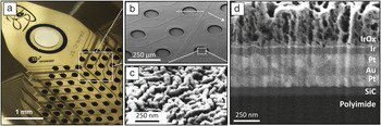
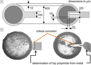
The charge injection capacity (CIC) of a metal defines how much electrical charge can be transferred through a specific area (units in C/cm2) before irreversible corrosion mechanisms (electrodissolution) come into effect.Reference Boretius, Jurzinsky, Koehler, Kerzenmacher, Hillebrecht and Stieglitz111–Reference Cogan, Edell, Guzelian, Ping Liu and Edell113 Depending on the application, specific amounts of charge have to be delivered in order to excite electrical activity in the nerves. Platinum has a much higher charge delivery capacity than gold, which makes it interesting for stimulation applications. On the other hand, the ductility and the electrical conductivity of gold are higher than those of platinum, which is thought to make gold favorable for applications with higher mechanical loads and for reducing the track electrical resistance, which reduces electrical power losses. Miniaturization reduces the geometrical electrode contact area, which in turn diminishes the amount of charge that can be passed through an electrode. If thin-film metallization is involved in corrosion due to too much charge being passed through the interface, it will disintegrate very quickly (Figure 3). To avoid corrosion, metalsReference Boretius, Jurzinsky, Koehler, Kerzenmacher, Hillebrecht and Stieglitz111, Reference Cogan, Edell, Guzelian, Ping Liu and Edell113 or conductive polymersReference Green, Lovell and Wallace114, Reference Green, Devillaine, Dodds, Matteucci, Chen, Byrnes-Preston, Poole-Warren, Lovell and Suaning115 with larger CIC (iridium oxide, iridium, platinum-iridium, or PEDOT [poly(3,4-ethylenedioxythiophene)]) are used instead of platinum or gold as active materials on the electrode sites. Alternatively, the surface is enlarged by roughening, creating a larger active surface than the geometrically given areaReference Boretius, Jurzinsky, Koehler, Kerzenmacher, Hillebrecht and Stieglitz111, Reference Ordonez, Boehler, Schuettler and Stieglitz116 (Figure 4).
The interface between metal and polymer is critical. The physical adhesion will be affected by water intrusion, while chemical adhesion that forms a bond to both materials should remain stable over time. A promising approach is with silicon carbide as an adhesion promoter for platinum/polyimide interfaces, which provides a non-metallic but stable chemical bond to both layers.Reference Ordonez, Boehler, Schuettler and Stieglitz130

(a) Optical image and (b) scanning electron micrograph of the stimulation sites of a thin-film polyimide electrode array for stimulation of the retina. The wires are coated with SiC to promote adhesion to the polyimide substrate, and the (c) active sites are coated with sputtered iridium oxide to achieve not only larger surfaces through the rough structure but to provide a safer electrical stimulation of the tissue. (d) The cross-section of the stimulation site shows the complex layer composition: SiC promotes adhesion of the Pt and the polyimide. Gold is used as a core in the Pt wires to reduce the overall electrical resistance of the metallic tracks. Ir and IrOx are sputtered onto the Pt to create a transition into a material with high charge delivery capacity and increased active surface area.Reference Ordonez, Boehler, Schuettler and Stieglitz129

PDMS-foil electrode arrays are in this sense much more resilient. They can be involved in non-reversible dissolution mechanisms, where there is “enough” metal that the loss of some nanometers will not lead to failure of the device. The mechanical and electrical stability of PDMS-based electrodes is what categorizes them as “robust,” with the sometimes-undesired disadvantage of thickness and size.
The problem of adhesion and delamination
Delamination of the layers in the wet body environment has been the major failure mode of thin-film micromachined devices. Fabricating a stable assemblage of metals and polymers is complicated, as it is not possible to make the polymer and the metal atoms mix and form a compound. When taking a closer look at the failure mechanism, especially in the case of polyimide-metal electrodes, White said in 1983, “The principal difficulty encountered by scientists, and others attempting to fabricate polymer-metal-polymer electrodes, is that of delamination.”Reference White, Roberts and Cotter117 Delamination during the usage of polyimide has continued to be a problem. Adding to the personal experiences of the authors, literature reveals that Ti/Au (1997 and 2009)Reference Henle, Meier, Schuettler, Boretius and Stieglitz46, Reference Shire, Kelly, Chen, Doyle, Gingerich, Cogan, Drohan, Mendoza, Theogarajan, Wyarr, Waler and Mason80 and platinum (2007)Reference Lago, Yoshida, Koch and Navarro43 still delaminate from polyimide. Even though there are various approaches for adhesion improvement (see later in text), none of them have provided the desired stability for long-term application so far. Furthermore, the quantitative comparison with reasonable large sample sizes and reliable statistics has not been properly assessed to date.
Since neural prostheses are implanted in the human body with its aqueous environment containing salts and proteins, interactions with these ions and molecules have to be taken into account. To some extent, all polymers are permeable to gases (including water vapor),Reference Buchhold, Nakladal, Gerlach and Sahre91 so it is not possible to avoid the intrusion of water molecules into the polymer-metal assemblage. Besides the diffusion of water, all polymers also absorb water to a material-specific degree, leading to a plasticizing effect in the polymer correlated to expansion of the polymer chains,Reference Buchhold, Nakladal, Gerlach, Sahre and Eichhorn90, Reference Buchhold, Nakladal, Gerlach and Sahre91 which permits further diffusion of other elements in the solution, such as ions or salts.
Water absorption alters the polymer-metal interface in two ways. First, it induces stretching. It has been shown that thin polyimide layers expand in-plane, however, after thorough analysis, Buchhold et al. have concluded that this humidity-induced coefficient of expansion is low for BPDA-PPD polyimide, compared to other types.,Reference Buchhold, Nakladal, Gerlach, Sahre and Eichhorn90, Reference Buchhold, Nakladal, Gerlach and Sahre91 Nevertheless, the stress that can be induced in an adjacent layer—described by the stress coupling factor—which depends on the Young’s modulus and Poisson’s ratio, can still be high. This can combine with the stress created in the assemblage due to the thermoelastic mismatch of the layers and the processing history of the device, for which the fabrication already subjects the plastic-polymer interface to internal stresses. If this stress reaches critical levels, it will lead to cracking or delamination, depending on whether the adhesion or the cohesion strength is higher, respectively.
Second, the absorbed water can affect the physical forces contributing to the bond between the layers. These forces decrease to the power of six with distance.Reference Woodruff118, Reference Gnanou and Fontanille119 Just a few water molecules are capable of fully eliminating any attraction between two surfaces (e.g., metal and polymer), not only by coming between them but also by being nearby and inducing polarity changes in the region. BPDA-PPD polyimides are the least polar of all polyimides, which is reflected by their water uptake being the lowest.Reference Malay and Mittal87, Reference Sacher and Susko120, Reference Sacher and Susko121 Any physical force contributing to adhesion will be affected if the polymer’s physical properties, such as polarity, are altered. Chemical adsorption, in contrast to the physical bonding, is defined by either covalent, ionic, or hydrogen bonds, which all lead to very strong binding.Reference Bruch, Cole and Zaremba108, Reference Woodruff118, Reference Gnanou and Fontanille119 In the chemical adsorption process, the surfaces of the materials react with each other, creating a new “intermaterial” layer that gives the bond strength and is naturally stable. This bond, in the best case, is unaffected by water.
The aftermath of delamination is critical in various aspects. Even if delamination only happens at the top metal-polymer interface, the metal is exposed to solution at undesired locations and will potentially allow the current flowing through the wire to transfer into the ionic solution at an undesired place. An increased current density at the wire where current is transferred into solution can lead to electro-dissolution of the thin filmReference Schuettler and Stieglitz112 (Figure 5). If the current is not a critical issue (as in the case of signal recordings), the leakage can go along the tracks to the interconnection sites, which are only rarely composed from identical metals. Consequently, galvanic corrosion is likely to happen at these sites. For gold/platinum interconnection contacts, which have only a very small difference in their galvanic potentials, no failure caused by galvanic corrosion has been reported in vivo so far. Beyond corrosion, if the metal layer is fully detached from the polymer substrate, any fractional force will break the metallic layers.
Top view of (a) design and (b) through-light microscopy images of thin-film platinum/polyimide electrodes after electrical loading.Reference Schuettler and Stieglitz112 The delamination of the polymer over the track is visible through Newton’s Rings. A large current density leads to critical dissolution of the metal at the exposed site and, given the delamination, at the track too. This is visible (b) at the lighter areas (exposed polyimide) in the image. All dimensions are in micrometers. Reprinted with permission from Reference Reference Schuettler and Stieglitz112.

Adhesion promotion techniques
The use of oxygen plasma has been successfully applied to roughen the polymer surface and achieve better interlocking of the thin-film metallic layer and the carrying substrate (mechanical adhesion).Reference Stieglitz8, Reference Lago, Yoshida, Koch and Navarro43, Reference Rubehn, Bosman, Oostenveld, Fries and Stieglitz44 Moreover, the oxygen concentration on the surface during the treatment increases surface activation, which alters the amount of carbonyl groups and creates reactive binding sites for the subsequently deposited metallization.Reference Murray and Hillman105, Reference Girardeaux, Druet, Demoncy and Delamar122, Reference Egitto, Matienzo, Blackwell and Knoll123 The observed adhesion strength comes from the formation of carbides at the polymer-metal interface.Reference Girardeaux, Druet, Demoncy and Delamar124 However, chemical adhesion is dependent on the reactive willingness of both partners involved. Gold and platinum have been widely used for tracks and contacts in micromachined neural interfaces, but in contrast to the transition metals titanium, chromium, nickel, and tungsten, which form carbides, neither Pt nor Au are capable of forming long-term stable carbides.Reference Ham and Lee125, Reference Harris126 This is why many research groups have reported on W-Ti, Ti, and Cr metallizations as adhesion-promoting layers for the Au or Pt metallizations in polyimide-based thin-film devices.Reference Gonzalez and Rodriguez78, Reference Murray and Hillman105, Reference Furman, Childs, Clearfield, Davis and Purushothaman127 These interlayers create chemical bonds through carbide formation at the polymer interface and an intermetallic transition to the metallization of interest. However, no one has reported a long-term stable application of these metallic adhesion promoters in implantable devices. Delamination still occurs. Furthermore, it is undesirable to have a bimetallic combination in an ionic solution, since electrochemistry due to half-cell potentials will induce corrosion of the less noble metal, leading to failure of the device while releasing potentially toxic agents into the biological environment.
The use of inorganic interlayer materials is the next consideration when the fabrication of corroding galvanic elements is to be avoided. Cogan et al. mentioned the use of silicon carbide as an insulating coating around goldReference Cogan64 or platinumReference Cogan, Edell, Guzelian, Ping Liu and Edell113 tracks. The reactivity of platinum with silicon is known,Reference Chou128 making silicon carbide an optimal interlayer material for adhesion promotion of platinum to polyimide or vice versaReference Ordonez, Boehler, Schuettler and Stieglitz116, Reference Ordonez, Boehler, Schuettler and Stieglitz129, Reference Ordonez, Boehler, Schuettler and Stieglitz130 (Figures 3 and 4). The polyimide is capable of establishing a carbon-carbon bond, while the platinum can also chemically adhere to the SiC. A quantitative analysis of the adhesion properties and the fundamental adhesion mechanism of this layer are currently under investigation by the authors, and initial studies have been presented.Reference Ordonez, Boehler, Schuettler and Stieglitz116, Reference Ordonez, Boehler, Schuettler and Stieglitz129, Reference Ordonez, Boehler, Schuettler and Stieglitz130
Parylene-C is known for its extremely high biological and chemical inertness, which correlates to major difficulties regarding adhesion to other materials such as metals.Reference Hassler and von Metzen131, Reference Chang, Lu and Tai132 Silane A-174 has been successfully used as an adhesion promoter, but it is known for its toxicity. Although its lethal dose is low (LD50 > 2000 mg/kg) and could be considered negligible, it is an ethical question whether the development of such devices with toxic agents should be pursued.
Summary and conclusions
Electrode arrays can be roughly separated into two types: flexible and stiff. Stiff arrays are based on silicon or ceramics and processed with common microelectromechanical systems methods such as photolithography, plasma deposition techniques of metals and inorganic layers, and reactive ion etching. These devices have great spatial resolution and can be used for penetration into deeper regions in the brain. Their main field of application is neuroscience, and the devices are commonly used in short-term (<1 year) studies. Flexible electrodes fabricated for application in medical devices can also be subdivided into two groups. First, silicone rubber arrays are associated with the disadvantage of limited integration density but have the advantage of comparably uncomplicated medical device approval. Second, microelectrode arrays made of polyimide or parylene are produced by application of MEMS fabrication techniques. Even though the fabrication of the latter requires large and complex machinery parks and long processing times, they yield smaller and more complex devices with higher integration capabilities. Diseases such as blindness, where the complexity of the biological system is extremely high and the implantation site is relatively small, rely on the use of such technologies. If more focus is set on the application of biostable inorganic layers as adhesion promotion for metallic layers and metals with large charge injection capacities for the active sites, technology will soon reach the necessary maturity to manufacture devices that provide the required stability, leaving aside corrosive metal combinations and toxic chemicals as adhesion promoters. For therapy and rehabilitation of diseases that have been so far resistant to treatment and fatal, it is essential to turn to translational research and bring these experimental devices into clinical applications.