Introduction
Metamaterials (MM) display unique phenomena, such as negative index, because of their engineered sub-wavelength structure. Our aim is to realize an all-dielectric metamaterial (ADM) operating in the terahertz (THz) range [Reference Luo, Yan and Zhou1]. Indeed, conventional MMs are built around a metallic unit cell, having a complex geometry, and they consequently suffer from ohmic losses that increase with frequency [Reference Dupas, Guillemet-Fritsch, Geffroy, Chartier, Baillergeau, Mangeney, Roux, Ganne, Marcellin, Degiron and Akmansoy2]. Differently, the unit cell of ADMs consists of two high permittivity resonators with simple geometry. The incident electromagnetic (EM) field excites the first two Mie resonances, which results in resonant effective permeability and permittivity, respectively. The superposition of the latter may lead to a negative or near-zero effective index neff. Ceramics, particularly those with high permittivity and low loss [Reference Matsumoto, Nakagawa, Kageyama, Wada and Sakabe3], are suitable for ADMs. In the terahertz range, the bulk ceramics has to be structured to the tens micrometers scale, with a precision of the micron, so as to sustain the resonances. Besides, THz radiation, defined between 0.1 and 10 THz, has various applications including imaging and sensing, as it provides unique physical phenomena. The targeted frequencies are 0.3 and 0.6 THz, because they correspond to windows of atmospheric transmission. We produced samples using  $\text{TiO}_{2}$ ceramic, chosen for its high permittivity and low loss. The bulk
 $\text{TiO}_{2}$ samples were fabricated from commercial powders and sintered using two different processes: conventional and spark plasma sintering (SPS). These samples were then characterized in the 0.2–1.4 THz range using THz time-domain spectroscopy (THz-TDS). We further looked for the best way to structure the bulk
 $\text{TiO}_{2}$ ceramics at the micron scale, to realize an ADM operating at THz, and then considered four different micro-structuring processes:
(i) micro-molding,
(ii) direct
 $\text{TiO}_{2}$ etching by inductively coupled plasma (ICP),
(iii) saw cutting and
(iv) femtosecond laser etching.

Specifically, we employed micro-machining for the devices aimed at 0.3 THz, whereas ICP etching was adopted for that targeting 0.6 THz. This manuscript reports on an exploratory work to find out a process to shape the bulk  $\text{TiO}_{2}$ material at the tens of micrometers with a one micrometer resolution. Currently,
 $\text{TiO}_{2}$ is shaped at the nanoscale or when it is in the form of a film a few hundred nanometers thick [Reference Saponjic, Dimitrijevic, Tiede, Goshe, Zuo, Chen, Barnard, Zapol, Curtiss and Rajh4–Reference Choi, Woo, Joo, Chun and Kim6]. An earlier version of this paper was presented at the 18th Conference of Antennas and Propagation (EuCAP 2024) and was published in its Proceedings [Reference Djemmah, Gourdonnaud, Geffroy, Roux, Bouamrane and Akmansoy7].
Experimental methods
Fabrication processes of the bulk material
The bulk  $\text{TiO}_{2}$ ceramic was obtained through two distinct sintering process: conventional sintering and SPS. In the conventional sintering process,
 $\text{TiO}_{2}$ powder is compacted using a die of 10 mm diameter under a compressive pressure of 50 MPa to form green compacts. These compacts are then sintered at
 $1550^{\circ} \text{C}$ during 30 min to produce a dense material.
Differently, during the SPS process, the  $\text{TiO}_{2}$ powder is placed in an 8 mm diameter graphite die. The material is then sintered using a high-intensity pulsed current at a temperature of
 $1150^{\circ} \text{C}$ and under a pressure of 10 MPa for a period of 5 minutes. Following the sintering processes, half of the samples were annealed in an ambient atmosphere, at temperatures set between 950∘ and
 $1100^{\circ} \text{C}$ during 60 hours. Lastly, the
 $\text{TiO}_{2}$ ceramic pellets were precisely polished to achieve a thickness ranging from 300 to
 $500\;\mu\text{m}$.
THz characterization
For the characterization of the polished ceramic pellets, we used a commercial Terapulse Lx spectrometer from TeraView™ [8]. This system is based on a femtosecond fiber laser operating at a repetition rate of 80 MHz. Its optical pulses are split into two paths by a beam splitter. One of these paths directs the pulses to the THz emitter (a photoconductive antenna), while the other leads to the THz detector. During measurement, the THz beam from the emitter passes through the sample located in a dry air chamber, in which the relative humidity is maintained below 10%. This beam is guided by four parabolic mirrors and its interaction with the sample is sampled using an optical delay line. The THz detector records the electric field as a function of time. This temporal signal then undergoes a Fast Fourier Transform to obtain the optical spectra. By comparing this transmitted signal with a reference signal, obtained without the sample, the spectra of the two signals can be calculated. From this data, we extract the complex refractive index  $n + i\kappa$ of the sample. Eventually, these values are used to determine the complex permittivity
 $\varepsilon* = \varepsilon' + i\varepsilon^{\prime\prime}$ [Reference Roux, Garet and Coutaz9, Reference Duvillaret, Garet and Coutaz10]. Before the characterization of the samples, the setup has been calibrated by the means of a BK7 glass plate. The schematic of this experimental setup is shown in Fig. 1 (A top view is shown in fig. 1 in the supplementary material file).
Schematic diagram of the experimental THz time-domain spectroscopy (THz-TDS) setup.

The experimental results, reported in Fig. 2, are in good agreement with those of [Reference Matsumoto, Nakagawa, Kageyama, Wada and Sakabe3, Reference Yu, Zeng, Yang, Donnan, Huang, Xiong, Mahajan, Shi, Ye, Binions and Tarakina11]; they are also in good agreements with the Four Parameters Semi-Quantum (FPSQ) model, which has been calculated using the permittivity  $\epsilon'$ of rutile (001) single crystal, which is isotropic. [Reference Matsumoto, Hosokura, Kageyama, Takagi, Sakabe and Hangyo12, Reference Djemmah, Geffroy, Chartier, Roux, Bouamrane and Akmansoy13] In the concerned frequency range, the real part
 $\varepsilon'$ of the permittivity linearly increases with the frequency, and the imaginary part
 $\varepsilon^{\prime\prime}$ almost linearly increases with the frequency, but it is higher than that of the FPSQ model. We assume that this is due to the concentration of oxygen vacancies VO and
 $\text{Ti}_{3}^{+}$ ions [Reference Setvín, Wagner, Schmid, Parkinson and Diebold14]. Moreover, the fabricated
 $\text{TiO}_{2}$ pellets are made from powder are polycrystalline, which means they are composed of numerous crystalline grains with random orientations. The interfaces between them, as well as possible impurities and defects in the material, may induce additional dielectric behaviors not accounted for in an idealized semi-quantum model (see also [Reference Djemmah, Geffroy, Chartier, Roux, Bouamrane and Akmansoy13]).
Comparison of the THz-TDS experimental data (circles) with those of the FPSQ model (solid line): real and imaginary parts of the dielectric function  $\varepsilon^*$.

Results and discussion
Influence of the type of sintering on the dielectric properties
For the successful realization of an ADM, we thus seek the most suitable process for manufacturing  $\text{TiO}_{2}$ pellets with a high permittivity (
 $\varepsilon' \simeq 100$) and a minimal loss factor (
 $\tan\delta \lesssim 0.02)$) from commercial powders [Reference Djemmah, Geffroy, Chartier, Roux, Bouamrane and Akmansoy13]. We explored both conventional sintering and SPS.
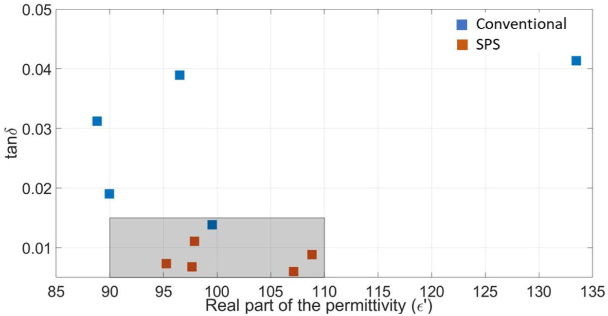
A total of ten samples were synthesized – one half using conventional sintering and the other half using SPS. The characterization by Time Domain THz Spectroscopy (TDS-THz), as reported in Fig. 3, shows that the samples produced by SPS (indicated in red) exhibit improved properties compared with those produced by conventional sintering (indicated in blue). XRD characterizations were carried out on some of the samples, showing that the synthesized  $\text{TiO}_{2}$ ceramic is of the rutile type.
Loss  $\tan\delta$ as a function of the real part
 $\varepsilon'$ of the permittivity at 0.3 THz for all the
 $\text{TiO}_{2}$ samples. Conventional sintering is indicated in blue, whereas SPS is in red. The shaded area highlights the samples whose the loss tangent is
 $\tan\delta \leq 0.015$ and the real permittivity is between 90 and 110.
 $\tan\delta \leq$ 0.015 is easily achieved by SPS.

Influence of annealing treatment on the dielectric loss
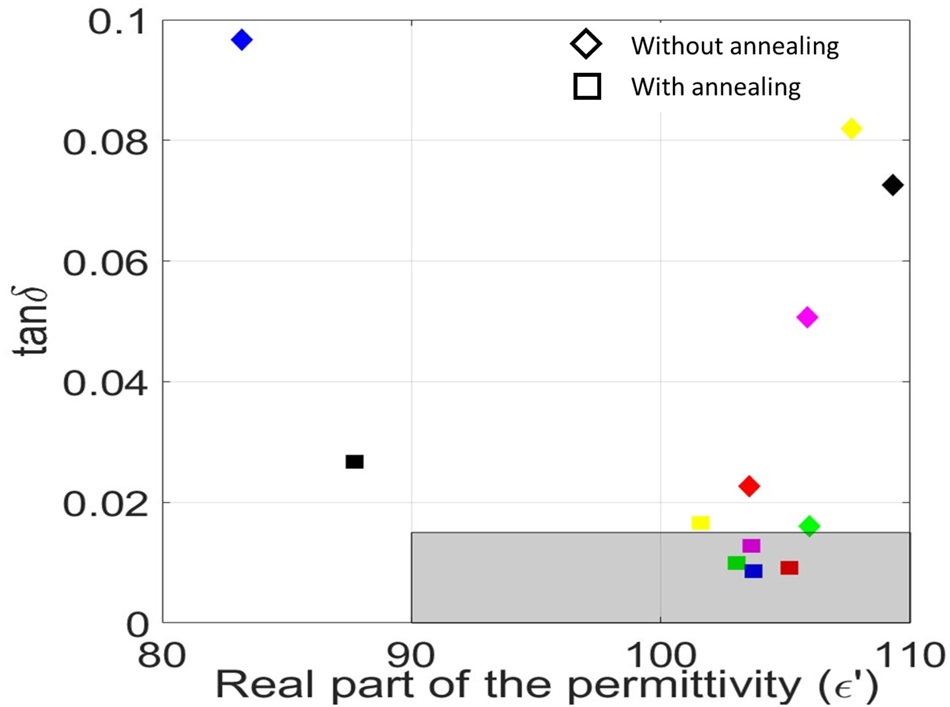
As the loss is an essential parameter to obtain the Mie resonances, we investigated the effect of annealing on this parameter. Twelve samples of two types were manufactured by pair under the same conditions (indicated by the same color), half annealed (indicated by square), half not (indicated by triangles) (see Fig. 4). The plot clearly shows that the annealed samples exhibit significantly lower dielectric losses ( $\tan\delta \leq$ 0.015 ) and a real part of permittivity between 90 and 110 at 0.3 THz. This result highlights the importance of this post-process, because during the SPS process, the material is subjected to high temperatures and pressure, which can result in the formation of defects. The latter can significantly affect the dielectric properties of the material. Annealing allows for reducing the concentration of defects in the material, particularly in terms of
 $\text{Ti}_{3}^{+}$ anomalies and oxygen vacancies.
The loss ( $\tan\delta$) as a function of real part (
 $\varepsilon'$) of the permittivity at 0.3 THz of
 $\text{TiO}_{2}$ samples elaborated by SPS with annealing (squares) and without annealing (triangles). The shaded area highlights the loss range corresponding to
 $\tan\delta \lt 0.015$ as well as the real permittivity value range of
 $\varepsilon'$ between 90 and 110, necessary to excite the Mie resonances.

Numerical simulation of the all-dielectric metamaterials
Based on these experimental results, we designed and simulated ADMs operating at THz frequencies. Their EM properties have been numerically simulated by the means of the Lumerical™ software, that involves the finite-difference time domain (FDTD) method; it yields the S-parameters from which the EM effective parameters (permeability, permittivity and index) are extracted. The simulations were specifically based on the measured characteristics of a  $\text{TiO}_{2}$ sample whose loss is
 $\tan\delta = 0.015$ at 0.3 THz, and its permittivity
 $\varepsilon_r = 102$. The elementary cell of the ADM comprises two 2D cylinders of TiO2, one having a rectangular cross-section (
 $58\;\mu\text{m}\times 110\;\mu\text{m}$) and the other having a square cross-section (
 $110\;\mu\text{m}\times 110\;\mu\text{m}$). The cylinders are arranged in a periodic pattern with a period of
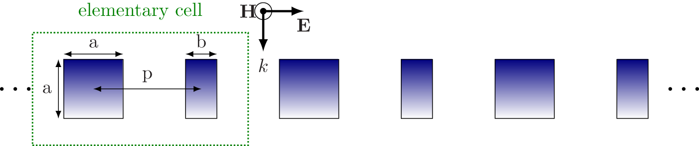
 $200\;\mu\text{m}$. The incident field is Transverse Electric (mode TE), the electric field being perpendicular to the axis of the cylinders. A schematic of the ADM is shown in Fig. 5.
Schematic of the 2D all-dielectric metamaterial. It is a periodic device, whose elementary cell consists of two height permittivity resonators, one having a rectangular cross-section (a × b) and the other having a square cross-section (a × a). The cylinders are arranged with a period p. The incident EM field is transverse electric.

The dimensions of these 2D resonators have been deduced from the Cohn’s model, which gives the frequency of the modes by the relation [Reference Cohn15]:
 \begin{equation}
f_{mn} = \frac{c}{2\sqrt{\varepsilon_r}} \sqrt{\left(\frac{m}{a } \right)^2 + \left(\frac{n}{b} \right)^2},
\end{equation}
where m and n are integers, and a and b are the dimensions of the sides of the 2D resonators. As we consider the first two modes of Mie resonances,  $m = n = 1$ and
 $m=1, n=2$ in the elementary cell, the first mode (denoted TE 11) being the magnetic one and the second (denoted TE 12), the electric one. Their respective frequencies are
 $f_{11} = 0.289$ THz and
 $f_{12} = 0.302$ THz.
Besides, ADMs exhibit negative effective index of refraction as Depine and Lakhtakia’s Condition (DLC) is satisfied [Reference Depine and Lakhtakia16], that is, when
 \begin{equation}
\varepsilon_{eff}'\,\mu_{eff}^{\prime\prime} + \varepsilon_{eff}^{\prime\prime}\,\mu_{eff}' \lt 0,
\end{equation}
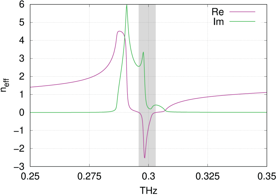
where the prime and the double prime denote the real and imaginary part, respectively. The simulation data, reported in Fig. 6, reveals that the first two Mie resonances are excited and lead to negative effective index neff (shaded area), whose minima is  $n_{eff_{min}}\: = -2.52$ at 0.298 THz, while its bandwidth is 7.1 GHz.
Numerical simulation of the effective index of an all-dielectric metamaterial. The dielectric properties used for the computation are derived from one of the characterized  $\text{TiO}_{2}$ samples: permittivity
 $\varepsilon' \simeq 102$ and losses
 $\tan\delta \simeq 0.015$ at 0.3 THz. The shaded region highlights the frequency range where the effective index is negative; its minimum is
 $n_{eff_{min}}\: = -2.52$ at 0.298 THz and its bandwidth is 7.1 GHz.

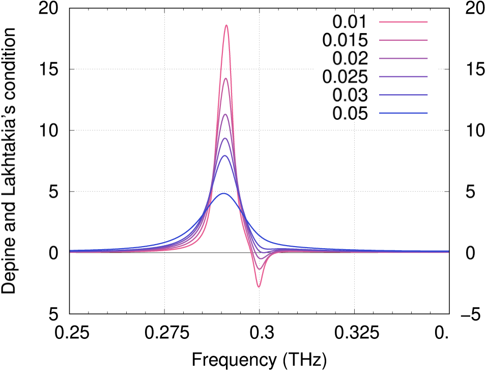
The maximal value of the loss to obtain negative effective index is determined from the DLC. In the case of  $\text{TiO}_{2}$, effective negative index is only achievable as
 $\tan\delta \lt 2\times10^{-2}$ (see Fig. 7).
 $\tan\delta \lt 15\times10^{-3}$ has been chosen as the critical value to ensure the negative effective index.
Depine and Lakhtakia’s condition as the loss is varied from  $\tan\delta = 0.01$ to 0.05. Effective negative index is only achieved as
 $\tan\delta \leq 0.02$.

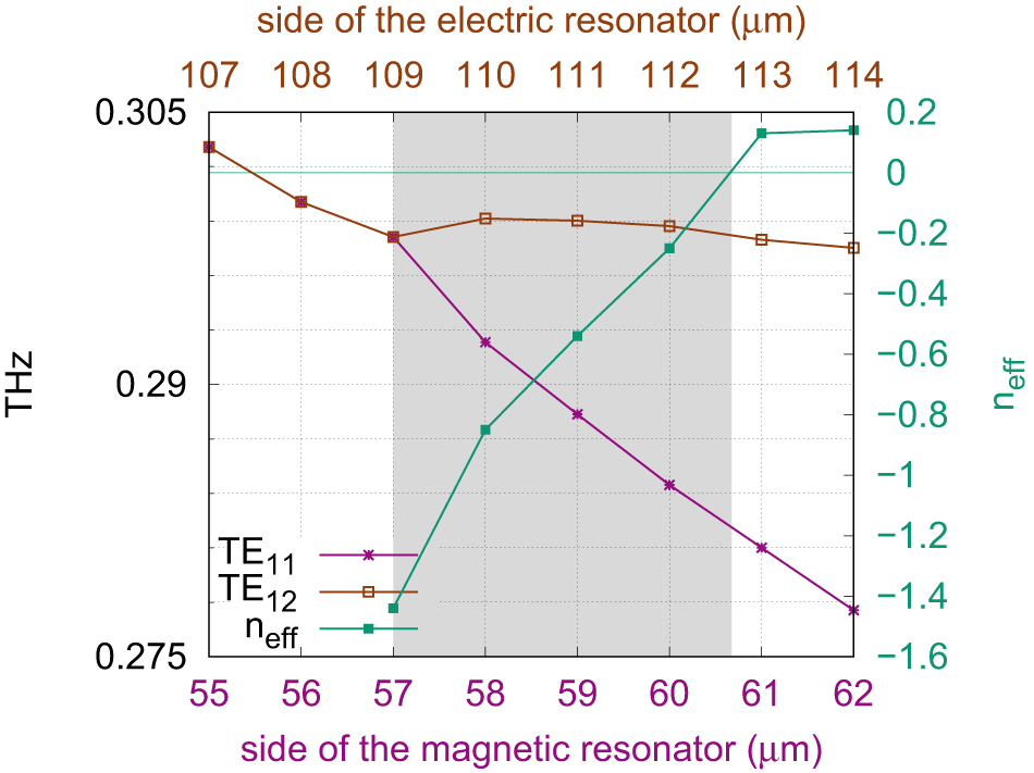
Coupling plays an important role in obtaining a negative index [Reference Akmansoy and Marcellin17]. Indeed, the first two modes of Mie resonance respectively result in a magnetic dipole and an electric one, that interact [Reference Lepetit, Akmansoy and Ganne18]. Modifying this coupling changes the effective index neff. For example, modifying one side of the resonators changes the frequencies of the modes of resonances (see equation (1)). Thus, by diminishing the same side of the two resonators of the unit cell, the frequency of the minima of the S 21-parameter of the first two modes increase until the two modes are degenerated, having the same frequency [Reference Akmansoy and Marcellin17] (see Fig. 8). Concomitantly, the effective index neff diminishes as the considered side diminishes, going from near zero values to negative values. As the modes are degenerated, the effective index is no longer defined [Reference Szabó, Park, Hedge and Li19]. A different unit cell, with different sizes but the same EM parameters, leading to a more negative value of the minimum of the  $n_{eff_{min}}\: = -3.6$ at 0.296 THz is reported in [Reference Djemmah, Gourdonnaud, Geffroy, Roux, Bouamrane and Akmansoy7]. Besides, a similar design and simulation have been carried out at 0.6 THz, also leading to negative effective index (see Fig. 1 in the supplementary material file). In that case, the elementary cell of the ADM comprises two 2D cylinders of TiO2, one having a rectangular cross-section (
 $28\;\mu\text{m}\times 55\;\mu\text{m}$) and the other having a square cross-section (
 $55\;\mu\text{m}\times 55\;\mu\text{m}$). The cylinders are arranged in a periodic pattern with a period of
 $120\;\mu\text{m}$.
Frequency of the minima of the S 21-parameter of the first two modes TE 11 and TE 12 in function of the side of the resonators. The frequencies of the two modes come closer as the same side of the resonators diminishes until they become equal; the two modes are then degenerated. Simultaneously, the effective index decreases, going from near zero values to negative ones (green curve). When the modes are degenerated, it is no longer defined.

Micro-structuration
Our aim is to realize 2D metasurfaces or 3D MM by the micro-structuration of bulk  $\text{TiO}_{2}$. In the fabrication of the devices, particularly for micro-structuring the bulk material, we explored four processes:
(i) micro-molding,
(ii) ICP etching,
(iii) femtosecond laser etching,
(iv) saw cutting.
The three last were carried out on rutile single crystal  $\text{TiO}_{2}$ pellets, with (001) optical axis orientation. Given the dimensions of the resonators, ICP etching is suited for ADMs targeting 0.6 THz, while the others processes are suited for 0.3 THz.
Micro-molding
Micro-molding, using polymer molds, is a microscale manufacturing process. This process has the advantage of facilitating the precise realization of components by accurately reproducing the specific characteristics of a polymer mold.
In this process, the fabrication of a high precision poly-methylmethacrylate (PMMA) mold was achieved by the means of deep x-ray lithography (DXRL) technology which can handle the requested high precision, i.e.,  $1\;\mu\text{m}$ precision for dimension and for positioning between structures (see Fig. 9). The theoretical precision of DXRL is mainly related to the vertical and horizontal divergences of the synchrotron source which are less than 0,1 mrad in our operating conditions, well beyond the required tolerance. X-ray lithography step was performed at Synchrotron SOLEIL, in Saint-Aubin (France) on Metrology beamline which is equipped with at dedicated scanner. The experimental process used is standard [Reference Bellanger, Brignon, Toulon, Primot, Bouamrane, Bouvet, Megtert, Quetel and Allain20]. Then the molds are filled with a commercial
 $\text{TiO}_{2}$ powder, combined with a binder. The next sintering stage is carried out at high temperature. During this process, the PMMA mold, whose melting point is around
 $200^{\circ} \text{C}$, undergoes combustion, which results in a dense
 $\text{TiO}_{2}$ part.
SEM picture of a PMMA mold done by X-ray lithography. Opening dimensions are 110 and  $60\;\mu\text{m}$, respectively, for a depth of
 $240\;\mu\text{m}$.

After the sintering, the next step is to extract this metadevice from its base component. This phase involves a meticulous operation to thin the base of the ceramic part, which initially served as the foundation for the patterning. To this end, the patterned side is wrapped in a protective resin matrix, such as epoxy. This epoxy resin layer plays an essential role, not only in keeping the ceramic bars in perfect alignment, but also in protecting them during subsequent operations, such as polishing.
Optical microscope images of a patterned device are reported in Fig. 10. The pattern seen in Fig. 10(a) and (b) is distinguished by a series of ceramic bars. Their width, height and spacing are approximately  $130\;\mu\text{m}$,
 $80\;\mu\text{m}$ and
 $75\;\mu\text{m}$, respectively, which matches the specifications of the PMMA mold used to produce this part. The depth of the LIGA etching was projected to be between 75 and
 $90\;\mu\text{m}$. Figure 10(c) displays the 3D measurement of the profile made along the y direction of the pattern. This figure demonstrates that the filling of the micro-cavities was correctly realized during the shaping of the part, with a regular crest height.
Optical microscope observations (a) in 2D of a  $\text{TiO}_{2}$ pattern structured by micro-molding and (b) 3D reconstruction of a part of the piece. from different viewing angles. (c) 3D measurement profile highlighting the structuration of the bulk material.

Since quartz is transparent in the considered THz range, it can also serve as a mold. The operating principle is the same; however, the mold will not be destroyed during sintering, its melting temperature being sufficiently high. Quartz will consequently serve as a support to the  $\text{TiO}_{2}$ part. We have already fabricated a quartz mold by Inductively Coupled Plasma–Reactive Ion Etching (ICP-RIE) process, similarly to the PMMA one and numerically simulated such an ADM.
Direct etching of
$\text{TiO}_{2}$ by inductively coupled plasma–reactive ion etching (ICP-RIE)

In this process,  $\text{TiO}_{2}$ is etched using a plasma source (ICP-RIE process), in a clean room. This process allows for direct etching of the desired pattern from the bulk material. Initially, a mono-crystalline
 $\text{TiO}_{2}$ pellet (Neyco brand,
 $500\;\mu\text{m}$ thick and (001) optical axis orientation) is first prepared by depositing a gold layer on the pellet, and then a photosensitive resin. By the means of an optical mask, the resin is exposed to reproduce the desired pattern and then Nickel is electroplated (see Fig. 11), which will protect the intended areas of
 $\text{TiO}_{2}$ during exposure to the plasma.
SEM (scanning electron microscopy) image of the patterned Nickel mask deposited on a mono-crystalline  $\text{TiO}_{2}$ pellet to protect it during the ICP-RIE etching.

The SEM (scanning electron microscope) images (see Fig. 12) reveal the success of the etching process: indeed an groove depth of  $59\;\mu\text{m}$ was etched into the pellet in a 140 min run (see Fig. 12(b)). This result is remarkable since only the etching of a few hundred nanometers in
 $\text{TiO}_{2}$ has been reported in the literature [Reference Joo, Woo and Kim21, Reference Park, Yoon and Yeonsang22]. It can be noticed from top to bottom: the Nickel mask, the bulk
 $\text{TiO}_{2}$, a passivation layer and the
 $\text{TiO}_{2}$ the bottom of the grooves, which have been characterized by Energy-dispersive X-ray spectroscopy (EDX). To finalize the device, polishing its back side of the
 $\text{TiO}_{2}$ will be necessary. For a successful operation, the patterned
 $\text{TiO}_{2}$ has to be wrapped in epoxy resin, the thickness of which eases handling for subsequent characterizations.
SEM (scanning electron microscopy) images of the  $\text{TiO}_{2}$ pellet after 140 min of ICP etching. (a) Left: View of the pattern etched; right: the two bars of the unit cell. (b) Zoom showing the
 $59\;\mu\text{m}$ high grooves between the
 $\text{TiO}_{2}$ bars. From top to bottom: the Ni mask,
 $\text{TiO}_{2}$, the passivation layer and the
 $\text{TiO}_{2}$ bottom of the grooves. (a)
 $\text{TiO}_{2}$ pellet patterned by ICP. (b) Depth of etching.

Saw cutting
This micro-structuring was carried out using a DISCO cutting equipment, model DAD 641. This equipment can cut wafers of various types (silicon, GaAs, glass, sapphire, etc.) and of various sizes from 200 to  $10\;\text{mm}^2$. The cutting blade is of the diamond resin type. Its thickness is
 $100\;\mu\text{m}$ and it is cooled under a water jet. One disadvantage of this process is that the grooves between the ceramic bars during cutting is set by the thickness of the blade, which sets the period of the pattern of the unit cell of the ADM. Currently, the thinnest blade available on the market for cutting
 $\text{TiO}_{2}$ is
 $100\;\mu\text{m}$ thick, which roughly corresponds to our needs. To limit splinters, the pellet has been coated with an epoxy resin. The results are shown in Fig. 13 and they demonstrate that this is a reliable and inexpensive process.
(a) Making grooves in a  $\text{TiO}_{2}$ substrate with a saw. (b) (Top left view): 3D visualization of the pattern cut into the substrate. (Top right view): top view of the sample showing the splinters made in the substrate during the sawing process. (Bottom view): depth profile of the pattern. (a) Tilted SEM images of the grooves fabricated on a
 $\text{TiO}_{2}$ substrate after removing the protective epoxy layer. (b) Microscopic 3D Keyence images.

Femtosecond laser etching
A  $\text{TiO}_{2}$ pellet has been etched by the means of a laser PERLA 100 (wavelength 1030 nm, power max. 100 W, pulse duration 1.5 ps, repetition rate 100 kHz) at Hilase Center [23]. A square basin with 6.4 mm large sides and
 $390\;\mu\text{m}$ depth was engraved in a mono-crystallin pellet (
 $10 \times 10\;\text{cm}^2$ large and
 $500\;\mu\text{m}$ thick). Then, grooves were cut in this basin to realize the
 $110\;\mu\text{m}+ 116\;\mu\text{m}+ 58\;\mu\text{m}+ 116\;\mu\text{m}$ pattern of
 $\text{TiO}_{2}$ bars with a
 $200\;\mu\text{m}$ period. The height of the bars is
 $110\;\mu\text{m}$. A photography of the etched sample and its profile are reported in Fig. 14.
Femtosecond laser etching of a mono-crystalline pellet (Hilase [23]). (a) Photography of the mono-crystallin  $\text{TiO}_{2}$ pellet (
 $10 \times 10\;\text{cm}^2$ large and
 $500\;\mu\text{m}$ thick) engraved and cut by femtosecond laser. (b) Topography image showing the etched pattern. (c) Depth profile of the
 $500\;\mu\text{m}$ thick pellet showing the engraved basin and the cut grooves realizing the pattern of the ADM.

Comparison of the processes
In this section, we compare three of the fabrication processes that can be used to fabricate devices operating at 0.3 THz. Getting the negative index requires the first two Mie resonances, meaning that the  $\text{TiO}_{2}$ bars sustain resonances. Some of their parameters have then to satisfy specific features: tolerance of about
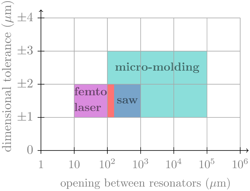
 $1\;\mu\text{m}$ on bars sides and their verticality has to be the closest to 90∘. The opening between two resonators is less important as it plays on the coupling of the modes, which is less strict (see Fig. 8). The tolerance versus the opening at 0.3 THz is reported in Fig. 15, based on estimated values, which shows that the three methods are suitable. Nevertheless, because a cross-section cut is needed, we could only measure the verticality in the case of the saw cutting, which is 91∘. The verticality is set by that of the mold, as micro-molding is involved.
Comparison of the micro-structuring processes at 0.3 THz. The red area is the targeted one.

Besides, because of the achieved etching depth ( $59\;\mu\text{m}$) (see section “Femtosecond Laser Etching”), the ICP-RIE process is consequently not currently usable for devices operating at 0.3 THz, whereas it could be at 0.6 THz. Indeed, the characteristic size of the unit cell is about
 $110\;\mu\text{m}$ at 0.3 THz, and about
 $55\;\mu\text{m}$ at 0.6 THz.
Conclusion
We have produced  $\text{TiO}_{2}$ ceramic samples for the realization of ADM operating at THz frequencies. By evaluating the two fabrication processes for these ceramics – conventional sintering and SPS – we studied the impact of post-annealing on SPS samples. These samples were characterized using THz TDS in the 0.2 to 1.4 THz spectrum. Our results indicate that the combination of SPS and annealing yields high-density
 $\text{TiO}_{2}$ samples with a permittivity of around 100. These possess low losses (
 $\tan\delta$ less than 2.10−2), making them suitable for ADM.
In addition, we explored four micro-structuring processes:
(i) micro-molding,
(ii) direct
$\text{TiO}_{2}$ etching by ICP,(iii) saw cutting, and
(iv) femtosecond laser etching.

The obtained results are promising. Micro-molding and saw cutting allows us to achieve vertical and parallel sidewalls. Besides, we have engraved, by ICP-RIE, a  $\text{TiO}_{2}$ pellet up to
 $59\;\mu\text{m}$ depth, which has not been yet reported. This last process could be suitable for devices operating around 0.6 THz.
Acknowledgements
D.A.D, F.L. and É.A. thank the French RENATECH network (specifically Thomas Tillocher @ GREMI – UMR 7344 CNRS). F.B. would like to thank P. Mercère and P. Da Silva for their support on the Metrology beamline at SOLEIL for the LIGA process.
Funding statement
D.A.D. thanks the MITI (Initiatives Transverses et Interdisciplinaires – CNRS) for financial support. This work has been funded by the French Agence Nationale de la Recherche (ANR) under DisPonT project.
Competing interests
None declared.

Djihad Amina Djemmah received a Master’s degree in Nanoscience and a PhD from Paris-Saclay University in 2020 and 2024, respectively. She is currently a postdoctoral researcher at the Institut des Nanotechnologies de Lyon (INL), where her work focuses on the development and optimization of advanced fabrication processes for nanoscale devices.

Fayçal Bouamrane, CNRS research engineer at Laboratoire Albert Fert, graduated in 1991 from the national engineering school, ENSI in Caen, France, in the field of materials science. He received a PhD degree from University Paris XI Orsay, in 1997, in materials science. Since 1998 he is using and developing the Deep X-Ray Lithography (DXRL) and related LIGA activity (German acronym for lithography, electrogrowth and molding). He is responsible of the lithography LIGA beam line at synchrotron SOLEIL since 2009. His research activity is focused on fabrication of X-rays dedicated micro-structures, in the field of THz technology as optical devices (multiplexers…) and more recently in processing all-dielectric meta-materials.

J.-F. Roux obtained his PhD from Grenoble University in 1995. In 1996, he became Associate Professor at the Université Savoie Mont Blanc (USMB) in the Department of Electrical Engineering. After defending his Habilitation in 2010, he was promoted to Professor in 2021. As a member of the CROMA laboratory (USMB, G-INP, UGA, CNRS), his research focuses both on optoelectronic components for THz signal generation and detection, and on the characterization of materials and devices for applications at THz frequencies. He is currently in charge of the Photonics Optics and Terahertz Optoelectronics group within this laboratory.

P.-M. Geffroy received his Ph.D. at the University of Bordeaux in 2005. He became researcher at French National Centre of Scientific Research (CNRS) at Institut of Research on Ceramics (IRCER) in 2006, and he is responsible of ceramic process research group at IRCER since 2020, as senior researcher. He is active in the study of innovative shaping processes and ceramic materials.

E. Akmansoy obtained his PhD and his Habilitation à Diriger des Recherche (HDR) from Université Paris-Saclay (Université Paris-Sud), where he is Associate Professor. He develops his research themes, which are about Photonic Crystals devices and Metamaterials, at the Centre de Nanosciences and Nanotechnologies (UMR 9001-CNRS).