Since the greatest interest in Si photonics have been demonstrated for telecommunication application, more applications have now emerged in the MIR wavelength range (2–5 µm) like gas sensing.[Reference Roelkens, Dave, Gassenq, Hattasan, Hu, Kuyken, Leo, Malik, Muneeb, Ryckeboer, Uvin, Hens, Baets, Shimura, Gencarelli, Vincent, Loo, Van Campenhout, Cerutti, Rodriguez, Tournié, Chen, Nedeljkovic, Mashanovich, Shen, Healy, Peacock, Liu, Osgood and Green1] Since SiO2 is transparent up to 3.5 µm wavelength,[Reference Soref2] silicon-on-insulator MIR spectrometers have been successfully demonstrated.[Reference Ryckeboer, Gassenq, Muneeb, Hattasan, Bogaerts, Cerutti, Rodriguez and Tournié3] For longer wavelength, Ge on Si platform is used.[Reference Barritault, Brun, Labeye, Hartmann, Boulila, Carras and Nicoletti4, Reference Malik, Muneeb, Shimura, Van Campenhout, Loo and Roelkens5] However, the monolithical integration of active devices (sources and photodetector) are still missing in MIR Si photonics. The current solution consists of growing[Reference Reboul, Cerutti, Rodriguez, Grech and Tournié6, Reference Wang, Tian, Pantouvaki, Guo, Absil, Van Campenhout, Merckling and Van Thourhout7] or bonding III–V materials[Reference Gassenq, Hattasan, Cerutti, Rodriguez, Tournié and Roelkens8, Reference Wang, Sprengel, Muneeb, Boehm, Baets, Amann and Roelkens9] on Si, which are not considered as complementary metal oxide semiconductor (CMOS) compatible by industrial foundries. For the group IV material sources, doped-Ge[Reference Liu, Sun, Camacho-Aguilera, Kimerling and Michel10] and GeSn alloys[Reference Wirths, Geiger, von den Driesch, Mussler, Stoica, Mantl, Ikonic, Luysberg, Chiussi, Hartmann, Sigg, Faist, Buca and Grützmacher11] are envisioned to obtain a CMOS compatible laser source. Note that GeSn devices are also studied for photo-detection applications on Si substrate.[Reference Gassenq, Gencarelli, Van Campenhout, Shimura, Loo, Narcy, Vincent and Roelkens12, Reference Pham, Du, Tran, Margetis, Tolle, Sun, Soref, Naseem, Li and Yu13] Strained-Ge structures also exhibits a MIR direct bandgap[Reference Geiger, Zabel, Marin, Gassenq, Hartmann, Widiez, Escalante, Guilloy, Pauc, Rouchon, Diaz, Tardif, Rieutord, Duchemin, Niquet, Reboud, Calvo, Chelnokov, Faist and Sigg14, Reference El Kurdi, Prost, Ghrib, Sauvage, Checoury, Beaudoin, Sagnes, Picardi, Ossikovski and Boucaud15] but their integration remains challenging. Such integration on a Si platform would open the way to MIR fully-integrated active devices (source and detectors), which are CMOS compatible. The availability of such approach would have many applications for sensing systems[Reference Soref2] or on-chip optical interconnects for high-performance computing.[Reference Zhou, Yin and Michel16]
In this work, we propose to bond highly-strained Ge directly on Si using a specific processing based on micro-bridge landing followed by the traction arm etching. Compared with free standing membranes, our landing approach will greatly facilitate the next process steps needed to go toward electrically pumped laser sources or integrated photodetectors based on strained-Ge for mid-infrared (MIR) applications. We measure a Raman spectral shift of around 8/cm corresponding to 4.2% in a Ge micro-block directly bonded on Si, which is higher than the first demonstration of 3 cm−1 using the biaxial approach.[Reference Sukhdeo, Petykiewicz, Gupta, Kim, Woo, Kim, Vučković, Saraswat and Nam17]
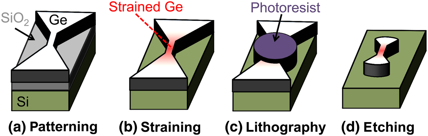
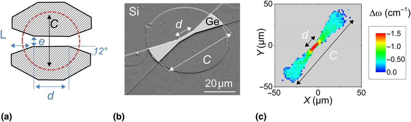
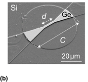
Figure 1 presents the device process flow. To amplify strain in the Ge, we have used the strain re-distribution principle[Reference Süess, Geiger, Minamisawa, Schiefler, Frigerio, Chrastina, Isella, Spolenak, Faist and Sigg18, Reference Gassenq, Guilloy, Osvaldo Dias, Pauc, Rouchon, Hartmann, Widiez, Tardif, Rieutord, Escalante, Duchemin, Niquet, Geiger, Zabel, Sigg, Faist, Chelnokov, Reboud and Calvo19] performed in 200 mm GeOI wafer.[Reference Reboud, Widiez, Hartmann, Osvaldo Dias, Fowler, Chelnokov, Gassenq, Guilloy, Pauc, Calvo, Geiger, Zabel, Faist and Sigg20, Reference Widiez, Hartmann, Mazen, Sollier, Veytizou, Bogumilowicz, Augendre, Martin, Gonzatti, Roure, Duvernay, Loup, Euvrard-Colnat, Seignard, Baron, Cipro, Bassani, Papon, Guedj, Huyet, Rivoire, Besson, Figuet, Schwarzenbach, Delprat and Signamarcheix21] The Ge layers are 0.35 µm thick on 1 µm SiO2 with Si substrate. Bridge patterning was performed using e-beam lithography followed by dry etching in an inductively coupled plasma reactor with Cl2, N2, and O2 gas [Fig. 1(a)]. After the Ge etching, the bridge lands on to the Si substrate[Reference Reboud, Gassenq, Guilloy, Osvaldo Dias, Pauc, Rouchon, Hartmann, Widiez, Tardif, Rieutord, Escalante, Duchemin, Niquet, Geiger, Zabel, Sigg, Faist, Chelnokov and Calvo22] using a low-speed under-etching recipe at 50 °C in a hydrogen fluoride (HF) vapor reactor [Fig. 1(b)]. Details about the SiO2 under etching recipes are given in Ref. Reference Gassenq, Tardif, Guilloy, Pauc, Bertrand, Rouchon, Hartmann, Widiez, Rothman, Niquet, Duchemin, Faist, Zabel, Sigg, Rieutord, Chelnokov, Reboud and Calvo23. The strain was thus tuned by the bridge design.[Reference Süess, Geiger, Minamisawa, Schiefler, Frigerio, Chrastina, Isella, Spolenak, Faist and Sigg18] The traction arms are then partially removed using a last lithography step [Fig. 1(c)], followed by the etching of the Ge [Fig. 1(d)]. The design parameters of the devices are presented in Fig. 2(a). Figure 2(b) presents a Scanning Electron Microscopy imaging of a fabricated device at the end of the processing when the Ge micro-block is directly bonded on the Si. The round layer corresponds to the last etching step [Fig. 1(d)], which was not selective between Ge and Si in this device.
Processing of (a) Ge layer patterning; (b) SiO2 under-etching leading to concentrate the strain in the centre of landed micro-bridge; (c) final lithography; and (d) to remove traction arms.

(a) Design parameter used to tune the strain in the Ge micro-bridge; (b) fabricated Ge micro-block landed/bonded on Si; (c) Raman spectroscopy mapping of a Ge micro-block bonded on Si, the strain is still concentrated in the narrowest part of the micro-block.
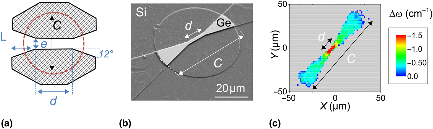
Figure 2(c) presents a Raman spectral shift mapping measured by micro-Raman spectroscopy on a Ge micro-block [e = 4 µm, L = 300 µm, d = 12 µm, and C = 100 µm in Fig. 2(b)]. The Raman spectral shift were measured with an input laser at 785 nm wavelength (given a measured depth of 200 nm[Reference Gassenq, Tardif, Guilloy, Duchemin, Dias, Pauc, Rouchon, Hartmann, Widiez, Escalante, Niquet, Geiger, Zabel, Sigg, Faist, Chelnokov, Rieutord, Reboud and Calvo24]) with a diameter spot of around 1 µm. The used laser intensity was low enough to avoid heating effect during the measurements.[Reference Süess, Minamisawa, Geiger, Bourdelle, Sigg and Spolenak25] Each Raman shift has been fitted using a Lorentz function. A bulk Ge substrate was used as reference to measure 0% strain to quantify the Raman spectral shifts, which increase with strain.[Reference Gassenq, Tardif, Guilloy, Duchemin, Pauc, Rouchon, Hartmann, Widiez, Niquet, Geiger, Zabel, Sigg, Faist, Chelnokov, Rieutord, Reboud and Calvo26] We observe here that the strain is concentrated in the central region, while the traction arms only undergo a much smaller strain, as observed for free standing membranes.[Reference Süess, Geiger, Minamisawa, Schiefler, Frigerio, Chrastina, Isella, Spolenak, Faist and Sigg18, Reference Minamisawa, Süess, Spolenak, Faist, David, Gobrecht, Bourdelle and Sigg27]
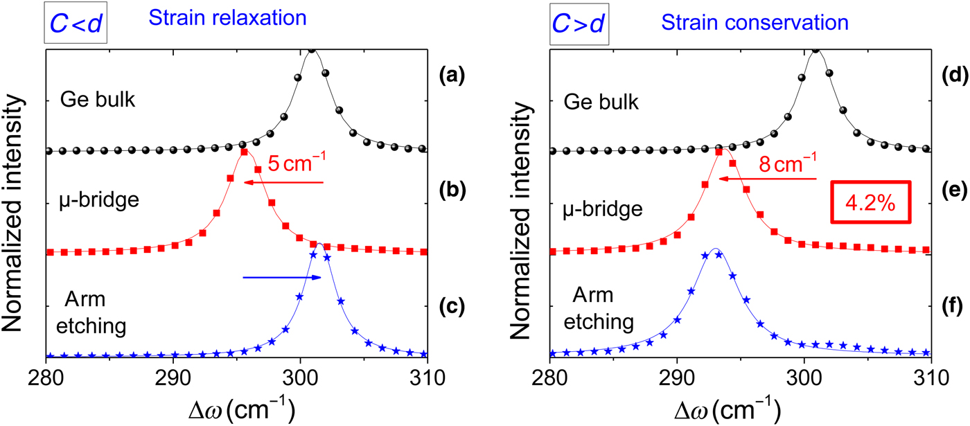
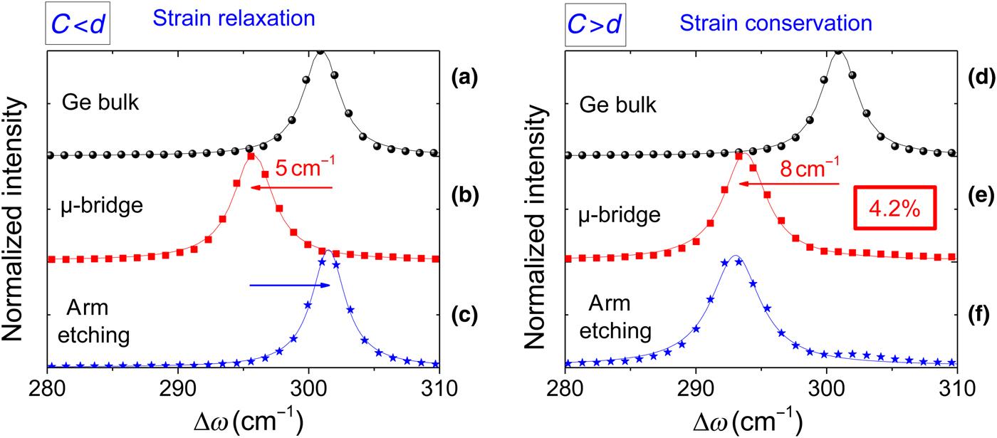
Figure 3 presents the Raman spectra before and after the arm removal for two representative designs: when the traction arms are completely removed [C < d in Fig. 2(a)] and when the traction arms are partially etched [C > d in Fig. 2(a)]. Figures 3(a)–3(c) present a micro-bridge with the following dimension e = 1 µm, L = 110 µm, d = 12 µm, and C = 10 µm. After the under-etching, the measured Raman spectra shift has been evaluated at 5/cm compared with the Ge [Figs. 3(a) and 3(b)]. The traction arms have been then fully removed, which results in a strain relaxation leading to a Raman spectrum close to bulk Ge [Fig. 3(c)]. Figures 3(d)–3(f) presents a micro-bridge with the following dimension e = 0.5 µm, L = 130 µm, d = 8 µm and C = 30 µm. After under-etching, the measured Raman spectra shift is evaluated to be 8/cm [Figs. 3(d) and 3(e)]. Then, we partially removed the traction arms. In that case, the strain is conserved [Fig. 3(f)] because of the bonding between the partial arms and the substrate, which is probably due to the small thermal annealing (50 °C), which occurs during the HF vapor under-etching. Therefore we obtain a Ge structure, which is bonded to the Si, with a very high strain of 4.2% (corresponding to a Raman shift of 8 cm−1[Reference Gassenq, Tardif, Guilloy, Duchemin, Dias, Pauc, Rouchon, Hartmann, Widiez, Escalante, Niquet, Geiger, Zabel, Sigg, Faist, Chelnokov, Rieutord, Reboud and Calvo24]). This value is very close to the actual maximum reported Ge strain of 4.9%[Reference Gassenq, Tardif, Guilloy, Duchemin, Dias, Pauc, Rouchon, Hartmann, Widiez, Escalante, Niquet, Geiger, Zabel, Sigg, Faist, Chelnokov, Rieutord, Reboud and Calvo24] and higher than the previous demonstration of 0.7% (3 cm−1) using the biaxial approach.[Reference Sukhdeo, Petykiewicz, Gupta, Kim, Woo, Kim, Vučković, Saraswat and Nam17]
Normalized Raman spectra of Ge bulk, Ge micro-bridge, and Ge micro-block with (a–c) the traction arms completely etched; and with (d–f) the traction arms partially etched.
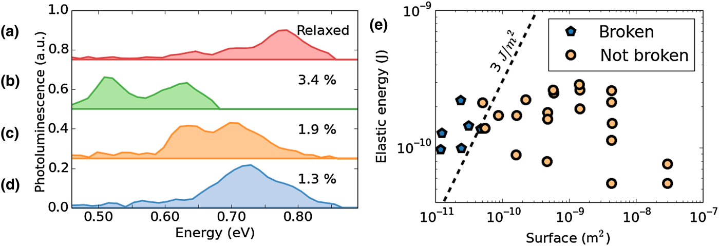
Photoluminescence (PL) measurements were also performed on strained-Ge micro-blocks. A 1047 nm Nd:YLF Q-switched laser, with an average power of 1 mW focused on an 20 µm diameter spot, was used to pump the material. The luminescence was collected through a Cassegrain objective and analyzed using a home-built Fourier Transform Infrared Spectroscopy spectrometer. A CdHgTe avalanche photodiode was used to detect the emitted light. Figure 4 shows the PL spectra of four Ge micro-blocks: a relaxed [Fig. 4(a)] and three differently strained Ge micro-blocks [Figs. 4(b)–4(d)]. Note that the PL measurements were not performed on the highest strained Ge micro-blocks presenting a Raman shift of 8/cm [Fig. 3(e)] as the dimension of the strained region are too small to obtain a correct PL signal with the sensitivity of our detection system. For strained samples two peaks are detected corresponding to the transition between the conduction band at Γ and the light- and heavy-hole valence bands.[Reference Guilloy, Pauc, Gassenq, Niquet, Escalante, Duchemin, Tardif, Osvaldo Dias, Rouchon, Widiez, Hartmann, Geiger, Zabel, Sigg, Faist, Chelnokov, Reboud and Calvo28] The strain is tuned here by the design of the micro-bridges[Reference Gassenq, Tardif, Guilloy, Duchemin, Dias, Pauc, Rouchon, Hartmann, Widiez, Escalante, Niquet, Geiger, Zabel, Sigg, Faist, Chelnokov, Rieutord, Reboud and Calvo24] up to 3.4% with a peak emission energy red-shifting when strain is increased, as expected.[Reference Süess, Geiger, Minamisawa, Schiefler, Frigerio, Chrastina, Isella, Spolenak, Faist and Sigg18] However, for strain-relaxed samples [Fig. 4(a)], the emission peak is shifted back at 0.80 eV, corresponding to the energy of the direct bandgap of unstrained Ge.
Photoluminescence spectra of integrated strained-Ge micro-block for (a) a relaxed sample and at (b) 3.4%, (c) 1.9%, and (d) 1.3%; (e) total surface of the micro-bridges plotted as a function of the total elastic energy of the stressed material. Samples marked in light yellow circle are strained, while samples marked in dark blue hexagon released their strain.
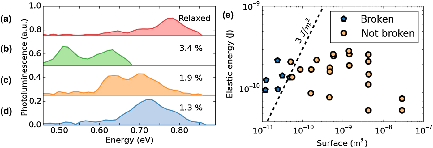
Figure 4(e) shows the elastic energy plotted as a function of the total surface (traction arms and strained area) of all devices. The elastic energy of their materials is written as:
 $$E = \raise.5ex\hbox{$\scriptstyle 1$}\kern-.1em/ \kern-.15em\lower.25ex\hbox{$\scriptstyle 2$} \sigma \varepsilon V,$$
where σ is the stress, ε the strain, and V the volume of the central region. We observe that the samples relax when the bonding surface is too small compared with the strain [dark blue hexagon of Fig. 4(e)]. The samples are expected to relax when their elastic energy, divided by the area in contact with the substrate, exceeds a certain threshold. From our set of samples, we estimate this elastic energy threshold to be at around 3 J/m2, which is in the same order of magnitude compared with the bonding energies measured by wafer bonding experiments.[Reference Fournel, Moriceau, Ventosa, Libralesso, Le Tiec, Signamarcheix and Rieutord29–Reference Gaudin, Riou, Landru, Tempesta, Radu, Sadaka, Winstel, Kinser and Hannon31] We hypothesize that further thermal annealing could increase this elastic energy threshold.
In this paper, we demonstrate the bonding of highly strained Ge structures to a Si substrate. A maximum of 4.2% induced strain is reported, which is reached by keeping partially the traction arm of landed Ge micro-bridges. This work allows envisioning compactly strained-Ge integration on Si for photonics applications.
Acknowledgments
The authors would like to thank the Plateforme de Technologie Amont and 41 in Grenoble for the clean room facilities and Dhruv Singhal for his language expertise. This work was supported by the CEA Phare project photonics.