


I. INTRODUCTION
Distributed amplifiers utilized in high bit-rate and wideband telecommunication have been traditionally dominated by compound semiconductor devices including InP, GaAs, or SiGe [Reference Schneider, Driad, Makon and Weimann1–Reference Aguirre and Plett5]. Recent advancement in digital CMOS technology with cut-off frequencies (f T) exceeding 100 GHz has enabled implementation of wideband CMOS distributed amplifiers [Reference Guan and Nguyen6–Reference Chien, Chen and Lu9]. In the distributed amplifier design, parasitic elements of active gain stage components are absorbed into distributed transmission lines or ladders of LC network (artificial transmission lines), resulting in wideband performance. In this multistage amplifier, as the signal propagates along the input line, it is sampled by each gain stage, amplified and collected constructively on the output line to provide a flat gain over a wide bandwidth. However, the low resistivity of the silicon substrate and its vicinity to the signal lines (due to thin oxide layer) causes additional parasitic components in the form of loss and distributed parasitic capacitance to the ground that degrade the performance of transmission lines and lumped inductors at high gigahertz frequencies. Attempts have been made to improve both gain and bandwidth of distributed amplifiers through compensating the losses of transmission lines by optimizing individual gain stages [Reference Mohammadi, Park, Pavlidis, Guyaux and Garcia3, Reference Guan and Nguyen6, Reference Heydari, Bohsali, Adabi and Niknejad10] using a matrix of amplifiers [Reference Chen, Chien and Lu11] and introducing a feedback in the design [Reference Arbabian and Niknejad8].
In this paper, we have utilized low-loss slow-wave shielded (SWS) coplanar waveguide (CPW) lines with floating shields [Reference Cheung and Long12] to attain high-gain-bandwidth product from a four-stage cascode distributed amplifier. In Section II, design and implementation of low-loss transmission lines on silicon substrate are discussed. In Section III, details of the implementation of the four-stage distributed amplifier are presented. Experimental characterization and analysis of the results are described in Section IV. Summary and concluding remarks are provided in Section V.
II. LOW-LOSS TRANSMISSION LINES ON SILICON SUBSTRATE
Multi-layer metallization in digital and RF CMOS technologies provide opportunities for implementation of microstrip, CPW, and other transmission line configurations shown in Fig. 1. For the microstrip line shown in Fig. 1(a), the distance between the signal and ground metal layer is set by the thickness of the oxide layer, typically around a few µm in most standard CMOS processes. In order to realize 50 Ω transmission lines, a narrow signal line (5–10 µm width for an oxide thickness of 3–5 µm) is required. Such lines are lossy and can be used for mm-wave frequencies (above 60 GHz) at which very short transmission lines typically in the order of a few hundred µm are needed [Reference Heydari, Bohsali, Adabi and Niknejad10, Reference Doan, Emami, Niknejad and Brodersen13]. For frequencies below 40 GHz, in lieu of microstrip line a CPW transmission line shown in Fig. 1(b) is preferred. CPW lines provide lower loss and higher Q on CMOS substrate (for the desired impedance range) compared to microstrip transmission lines [Reference Doan, Emami, Niknejad and Brodersen13]. The characteristic impedance of the CPW line is set by the width of the center conductor (S) and the gap between the center conductor and adjacent ground conductors (Gap), with insignificant contribution from the thickness of the substrate/oxide layer. The width of the center conductor can be increased beyond 5–10 µm to achieve low conductor loss for the transmission line. For a desired characteristic impedance of the line, however, wider lines require larger “Gap” spacing between the signal and ground metal traces. The widening of the center conductor increases the shunt parasitic to the substrate resulting in higher dielectric loss of the line. The dielectric loss is due to penetration of electromagnetic fields into the low-resistivity silicon substrate which cannot be avoided in the standard CPW structure. On the other hand, grounded CPW line (GCPW), depicted in Fig. 1(c) eliminates the substrate loss through the shielding provided by a continuous metal layer underneath the CPW line. Even though the substrate loss is minimized, the continuous ground plane of the bottom ground is prone to voltage fluctuations. The architecture shown in Fig. 1(d) eliminates the voltage fluctuations, by connecting the bottom ground plane to the top metal traces and forcing the voltages to balance out. Conversely due to the perpendicular component of the magnetic current of the CPW line, eddy currents are generated in the continuous metallic plane. This phenomenon that causes ohmic loss and generates heat in the conductor, adds to the conductor loss especially at higher frequencies in both of these configuration of lines, Figs 1(c) and 1(d) [Reference Ma, Rejaei and Zhuang14]. Alternatively in the architecture shown in Fig. 1(e) thin floating strips of metal underneath the CPW line isolate the signal line from the Si substrate, while it significantly reduces formation of eddy currents and hence the conductor losses. This architecture is also known as SWS CPW line. High-frequency structure simulator (HFSS) is used to demonstrate the electromagnetic field distributions for some of these transmission lines. Figure 2(a) depicts the cross-sectional view of the density of electric field for conventional CPW line along with its dimensions. The electric field distribution of GCPW is captured by HFSS in Fig. 2(b) that shows complete elimination of electric field impinging in the substrate underneath the continuous metal plate. Figure 2(c) depicts the electric field density of the SWS CPW line. The shielding strips are very narrow (<a few µm) to suppress eddy currents that may form in them. The spacing between the shield strips is very small to block most of the electromagnetic field from penetration into the substrate. By placing these strips under the CPW line the capacitance of the line increases. Hence a given length of the line with shielding strips appears to be longer for a given frequency, compared to a line without the shielding strips  . This phenomenon resembles a reduction in the speed of traveling wave and hence is called a slow wave transmission line. In other words, one can claim that this is equivalent to an increase in the effective dielectric constant of the line [Reference Cheung and Long12]. An alternative approach for shielding the signal line from the lossy substrate and reducing the conductor loss is depicted in Fig. 1(f) that uses a double layer of overlaying metal patches that sandwich a thin dielectric in between (can be oxide or any other thin dielectric). As demonstrated in [Reference Ma, Rejaei and Zhuang14], this so-called artificial dielectric layer (ADL) virtually increases the dielectric constant of the thin dielectric layer and stops the fields from impinging into the lossy substrate. This happens when the dimension of the square patches is much larger than the spacing between the patches (however much smaller compared to wavelength at operation frequency) [Reference Ma, Rejaei and Zhuang14]. Even though this method is useful, the size of patches is limited by design (15 µm demonstrated in [Reference Ma, Rejaei and Zhuang14]) compared to the floating shielding strips (1 µm as shown in Fig. 1(e)). Hence ADL will still be relatively lossy at high frequencies where the formation of eddy current flow is not negligible.
Different transmission line configurations on silicon substrate: (a) microstrip line, (b) CPW line, (c) GCPW, (d) shielded CPW, (e) SWS CPW line, and (f) ADL for shielding CPW line.

Magnitude of electric field of (a) CPW line (b) GCPW, and (c) CPW line with floating strips of shielding (SWS).

In this work, a standard 0.13 µm CMOS technology with six thin metal layers (M1–M6) and a top thick Al metal layer (M7) with a thickness of about 0.6 µm is utilized to implement shielded transmission lines shown in Fig. 1(e). The bottom metal layer (M1) is used to implement shielding strips where as the top metal layer (M7) is used for implementing the signal and ground traces of the CPW line. The distance between the top metal layer (M7) and the bottom layer (M1) is about 6 µm. SiO2 filled with small filler metal patterns (M2–M6) is used as the dielectric layer. Filler metal patterns are required to achieve planarity at each metallization step in order to obtain high yields in submicron fabrication. For simulation purpose the effect of the metal fillers is neglected, due to their relative small size in comparison to the effective wavelength up to mm-wave frequencies. The simulations are validated by comparison with measurements.
Figure 3 demonstrates the HFSS simulation and measurement results for the S-parameters of a 1 mm long 50 Ω shielded CPW line with S–Gap–ground dimensions of 10 µm–10 µm–85 µm with shield metal width gap of 1 µm–1 µm. The simulations are performed in HFSS V.10 and they are in good agreement with measurement results. Figure 3 also shows a standard 50 Ω CPW line without shielding (S–Gap–ground: 35 µm–10 µm–70 µm) on the same substrate. There is about 0.24 dB per millimeter improvement in the insertion loss response at 10 GHz when floating shield strips are used. As expected simulations show that GCPW line has a better insertion loss compared to that of a conventional CPW line, whereas it has higher loss compared to SWS CPW line. This is mainly due to eddy current formation and dissipation of energy in form of heat and conductor loss. The reflection losses (S 11)s are close (below −15 dB) as all the lines are designed to have characteristic impedance of 50 Ω. This SWS CPW line is used for the design and implementation of the wide-band distributed amplifier discussed in the next section.
S-parameter measurement and simulation for various 50 Ω CPW lines indicated in Fig. 2 on CMOS substrate: (a) insertion loss and (b) return loss.

III. DISTRIBUTED AMPLIFIER DESIGN
In traditional multi-stage amplifier design there is always a trade-off between the gain and bandwidth of the amplifier. In conventional parallelization of amplifiers (or gain stages) adding more amplifier stages will increase the gain while the bandwidth decreases, keeping the gain-bandwidth product almost constant. While in a distributed amplifier design approach the gain-bandwidth product increases towards a theoretical limit of the cut-off frequency (f T) of gain stages. This is due to the fact that the input capacitances are not directly in parallel, as are in the conventional parallelization case. In distributed amplifier architecture, the input capacitance of each stage is absorbed by gate transmission lines therefore, if designed correctly, the transconductance (g m) of stages, are added together constructively. Hence as the number of stages increases, the bandwidth remains unchanged while the gain increases; resulting in a large gain-bandwidth product despite a delay introduced by long transmission lines.
The circuit schematic of a four-stage CMOS cascode distributed amplifier implemented here is shown in Fig. 4(a). All the transmission lines used in the structure are based on SWS structure as shown in Fig. 1(e). Figure 4(b) depicts the microphotograph of the chip fabricated using standard 0.13 µm CMOS process. The amplifier including its DC and RF probe pads occupies a total area of about 2.58 mm2.
(a) Schematic of the proposed four-stage distributed amplifier with cascode gain stages. All transistors are identical with sizes of 60 fingers, each 2 µm wide and 0.12 µm long. (b) Microphotograph of the chip occupying a total area of 2.85 mm2 including DC and RF pads.

Cascode gain stage used in this amplifier provides similar gain for a relatively wider bandwidth compared to a single common-source transistor gain stage while it maintains a better isolation between the input and output lines and higher impedance at the output.
It is shown that for an N-stage distributed amplifier with identical stages and negligible loss on the drain line (due to utilizing cascode gain stages), the power gain of the amplifier can be expressed as the following equation [Reference Ayasli, Mozzi, Vorhaus, Reynolds and Pucel15]:

where g m is the trans-conductance of each gain stage, Z D and Z G are the characteristic impedance of the drain and gate transmission lines (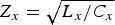 , where L x and C x are the corresponding inductance and capacitance per unit length of the transmission line x), N is the number of stages, l g i and l d i are the lengths of each section of gate line and drain line, respectively. γg and γd are the propagation constants of the gate and drain transmission lines defined in equations (2) and (3):


In the above equations L g and C g are the inductance and capacitance components of the gate transmission line, r g and C gs are the series resistance at the gate and the source-gate capacitance of common source transistor, respectively. C ds is the drain–source capacitance of the common gate transistor and R D is the resistance seen from the drain of the common gate transistor. In a cascode cell, the output resistance becomes much larger than a single common-source stage and hence in the distributed amplifier configuration based on cascode cells, the losses on the drain line are expected to be negligible ( ). On the other hand, under normal operating conditions phase velocity on the gate and drain line is matched (βgl g ≅ βdl d). Assuming αgl gN ≤ 1, one can simplify equation (1) as the following:

The first term in equation (4) (i.e. g m2 Z D Z G N 2/4) can be used as a guideline to calculate transistor size and biasing conditions (therefore g m of each gain stage) and the number of stages for a specific amplifier power gain. In this design the optimum transistor size for cascode cells are NMOS devices with 60 fingers, each 2 µm wide and 0.12 µm long. The two-port S-parameter measurement of the cascode gain cell up to 20 GHz is shown in Fig. 5. The bias conditions are V dd = 1.5 V, V Bias = 0.62 V, and V Gate = 1.5 V where the cascode current is about 8.7 mA; this corresponds to C gs of about 8.3 pf.
Measured two-port S-parameter of the cascode gain cell for V dd = 1.5 V, V Bias = 0.62 V, and V Gate = 1.5 V where the cascode current is 8.7 mA.

Equation (4) also suggests that the power gain does not increase monotonically when the number of stages, N increases. In fact, there would be an optimum number of stages N ≤ 2/r gω2C gs2 Z 0 that result in maximum gain. This is mainly due to the losses of gate transmission lines that counteract the gain produced by increasing the number of amplifying sections. Traditionally, there is no variation in the length of gate and drain sections. To maintain maximum gain flatness, however, the length of each section is optimized separately as shown in Fig. 4 [Reference Mohammadi, Park, Pavlidis, Guyaux and Garcia3].
Since the circuit incorporates both distributed and lumped components it was not possible to accurately simulate the entire amplifier during the design phase. Hence at first shielded transmission lines and junctions are simulated separately using Ansoft HFSS and modeled in Agilent ADS. Then the complete circuit including the active components and the modeled passive components are simulated and optimized within the expected bandwidth using ADS. The transistor models and parameter are extracted from Spectre/Cadence. Final design simulations are performed in ADS, while the length of each section is adjusted for the widest bandwidth and gain flatness.
IV. DISTRIBUTED AMPLIFIER CHARACTERIZATION
The four-stage CMOS distributed amplifier with SWS transmission lines is characterized using on-wafer probing under two conditions: low and high bias modes. In the low bias mode, the amplifier is biased with a V dd of 1.15 V a V Bias of 0.52 V, and a V Gate of 1.15 V where the current in each cascode gain stage is approximately 4.5 mA. In the high bias mode, the amplifier has a V dd = 2.2 V, V Bias = 0.62 V, and V Gate = 2.2 V. The current in each cascode gain stage in this case is approximately 11.5 mA. Agilent 8722 network analyzer is used for small-signal S-parameter measurements of the amplifier shown in Fig. 6. In the low bias mode the circuit dissipates 21 mW of DC power, with a forward transmission gain (S 21) of 7.6 dB (6.6 ± 1 dB) and a 3-dB bandwidth of 14.8 GHz. In the high bias mode and with DC power consumption of approximately 100 mW a S 21 gain of 12.8 dB (11.3 ± 1.5 dB) and a 3-dB bandwidth of 17 GHz are achieved. The simulations responses of the amplifier under both biasing conditions are shown in Fig. 6 which agrees with the measurement results at lower to mid-frequencies. At higher frequencies, however, the expected bandwidth derived from simulations is wider than that of the measurements. This can be contributed from few possible sources: (i) parasitic that are generated in the final layout of the amplifier and are not compensated for during simulation, including the metal fillers, (ii) limited bandwidth of the lumped model for the transmission lines that are extracted from simulations, and (iii) inaccuracies of large signal model of active cells at high frequencies. In [Reference Heydari16] it is suggested that the layout of transistors in terms of gate shape and gate resistance can be optimized to a “round-table” configuration to achieve higher maximum oscillation frequency ( improvement of ~70% is achieved). The optimized transistor layout similar to the one proposed in [Reference Heydari16] can be utilized in the future design to go along with optimized shielded transmission lines implemented in this work for a more matured design with much increased gain bandwidth product for CMOS distributed amplifiers. A measured group delay of about 42 ps across most of the bandwidth is extracted from the measurement of the phase of forward transmission gain, ∠S 21 under high bias condition as shown in Fig. 7. Since the network analyzer has been calibrated with SOLT calibration kit, the phase accuracy tends to degrade at higher end of the measurement range. Hence despite small phase nonlinearities of the amplifier, some fluctuation are observed when the group delay is extracted from phase measurements.
Measured and simulated S-parameter of the fabricated four-stage distributed amplifier in two conditions: (a) high bias condition (V dd = 2.2 V, V Bias = 0.62 V, and V Gate = 2.2 V) and (b) low bias condition (V dd = 1.15 V, V Bias = 0.52 V, and V Gate = 1.15 V).

Measured and simulated group delay of the distributed amplifier.

The linearity of the CMOS distributed amplifier is investigated using a one-tone linearity measurement with an Agilent 8360L signal generator and an Agilent E4448A spectrum analyzer. By keeping the input frequency constant while increasing the input signal power level the output spectrum is observed. The measurement is repeated for various frequencies within the bandwidth of the amplifier. Figure 8(a) depicts the output power as a function of the input power for three individual frequency points of 4, 10, and 14 GHz. Output-referred 1-dB compression points of +2.8, +2.27, and +2.02 dBm are measured for the amplifier biased under high bias condition at frequencies of 4, 10, and 14 GHz, respectively. Both input- and output-referred 1-dB compression points are also measured for various frequencies and are plotted in Fig. 8(b).
(a) Measured output power versus input power at 4, 10, and 14 GHz for 1-dB compression analysis with exemplary P1 dB extraction for 4 GHz case, and (b) input and output 1-dB compression points measured at different frequencies.

As shown in Fig. 9 the noise figure (NF) of the amplifier is also measured under both low and high bias conditions using Agilent N8975A NF analyzer under a 50 Ω source impedance environment. A minimum NF of 5.3 dB at 1 GHz is measured whereas the NF is below 8.5 dB for frequencies up to 10 GHz. The weak dependence of the NF to the biasing condition is likely due the fact that the NF is dominated by the loss of the input (gate) transmission line. In addition, good matching and low loss input section enhances the NF performance of the amplifier overall. Simulated NF of the amplifier under high bias condition is also shown in the figure with similar trends with the measured NF values.
Measured NF of the amplifier in two bias conditions (high current mode (V dd = 2.2 V, V Bias = 0.62 V, and V Gate = 2.2 V) and low current mode (V dd = 1.15 V, V Bias = 0.52 V, and V Gate = 1.15 V)) along with the simulation response of the Spectre/Cadence for the high current mode.

Table 1 summarizes the performance of this amplifier under these two bias conditions along with several state of the art CMOS distributed amplifiers implemented using CPW transmission lines. It is seen that with competitive power consumption, this amplifier provides a decent gain-bandwidth product (GBP), NF and 1-dB compression point. The performance can be further enhanced by utilizing a more accurate transistor model and optimizing transistor layout to reduce the gate parasitic resistances.
Performance summary and comparison with the state of the art distributed amplifiers in CMOS*.

* Data reported in this table are either provided in text, or derived from the plots or calculated from the available reported data.
†TL: transmission line, artificial: utilizing lumped L and C components; CPW: coplanar waveguide.
V. CONCLUSION
A four-stage distributed amplifier with low-loss SWS CPW transmission lines and cascode cells is implemented using standard 0.13 µm CMOS technology. The shielding of CPW lines from the lossy Si substrate is achieved by utilizing floating narrow strips of metals perpendicular to the traveling signal path. This shielding technique, not only reduces the substrate loss by almost 50%, it also creates a slow wave phenomena where shorter length of lines can be used (shorter by about 5% in our design). The amplifier is measured under two different bias conditions. In high current mode it provides a gain of 12.8 dB with 1.5 dB of ripples and a 3-dB bandwidth of 17 GHz when consuming 46 mA from 2.2 V power supply. A gain of 6.6 ± 1 dB up to a 3-dB bandwidth of 14.8 GHz is achieved with 18 mA from a 1.15 V power supply in the low bias mode. An NF of better than 8.6 dB up to 10 GHz is measured and is mainly due to the losses of the gate transmission lines. Linearity measurements reveal that the output-referred 1-dB compression point is +2.5 ± 0.5 dB across the bandwidth of the amplifier.
ACKNOWLEDGEMENT
This work was supported in part by the US National Science Foundation project ECCS 0802178.
 Rosa R. Lahiji received her M.S. and Ph.D. degrees in electrical engineering from University of Michigan in 2003 and Purdue University in 2009, respectively, with emphasis on 3-D integration and packaging of RFICs. She is currently a research associate at Case Western Reserve University and a Research fellow with West Wireless Health Institute where her research focuses on circuits, sensors, and systems for wireless health monitoring, telemedicine, and biomedical applications. Dr. Lahiji is the recipient of numerous awards for excellence and innovation in research and teaching and ranked 2nd place in student paper competition in IEEE Topical Meeting on Silicon Monolithic Integrated Circuits in RF Systems (SiRF 2009). She has published numerous papers in IEEE journals and conferences and has served as a technical reviewer for several IEEE publications including MWCL, ISCAS, JEMWA, and PIER Letters.
 Linda P. B. Katehi received master's and doctoral degrees in electrical engineering from the University of California at Los Angeles (UCLA), in 1981 and 1984, respectively. As of August 2009 she is Chancellor of the University of California at Davis (UC Davis) and holds faculty appointments in electrical and computer engineering and women and gender studies. She has mentored over 70 postdoctoral fellows and students, authored/coauthored 10 book chapters and approximately 600 refereed publications and holds 16 US patents. Her research is focused on the development and characterization of 3-D integration and packaging of integrated circuits with a particular emphasis on microelectromechanical systems devices, high-Q evanescent-mode filters, and the theoretical and experimental study of planar circuits. She is a member of the National Academy of Engineering as well as many other national boards and committees. She has been the recipient of numerous national and international awards both as a technical leader and educator.
 Saeed Mohammadi received his Ph.D. degree in electrical engineering from the University of Michigan in 2000. He is currently an associate professor of electrical and computer engineering at Purdue University. His group is currently involved in research in RF devices and circuits, RF packaging, and nanoelectronic technology. He has published more than 100 journals and refereed conference papers in these areas.