I. INTRODUCTION
Coupled Microstrip (CMS) line is one of several planar transmission lines used in integrated microwave circuits and components, such as filters [Reference Garcia-Garcia1] and directional couplers [Reference Islam, Elek and Eleftheriades2]. The CMS line is also used to drive high-speed microwave photonic components built on thin-film polymers, such as all-optical analog-to-digital converters (AOADC) based on electro-optical (EO) deflector [Reference Daryoush, Hou and Rosen3] and optical modulators [Reference Enokihara, Yajima, Kosaki, Murata and Okamura4]. Since coplanar waveguide (CPW) probes are primarily used in integrated planar circuit realization, broadband transitions from CPW to CMS lines [Reference Hadjloum, El-Gibari, Ginestar, Li and Daryoush5] are required in microwave photonic devices. A low insertion loss and flat group delay with low reflections at transitions interfaces is required over a large bandwidth for this transition to be applicable for opto-electronic devices that are considered in multiband or wideband applications [Reference Sun, Zhang, Receveur, Poddar, Rohde and Daryoush6].
For the example of CMS line in EO deflector [Reference Hadjloum, El Gibari, Gundel, Li and Daryoush7], the optical wave-guiding and the traveling wave radiofrequency (RF) electrodes are co-propagating to obtain optimal field overlap between lightwave and RF signals. Moreover, the CMS configuration reduces the number of technological steps required by manufacturing both optical core and RF strips at the same technological step using the micro-imprint contact technique [Reference Gates8]. However, to sample the applied RF signals provided from coaxial probes to CPW lines, short optical pulses are to be coupled from single-mode fiber to optical core from a mode locked laser. Because of mechanical alignment challenges, the optical energy and RF signal cannot be accessed on the same side. Therefore, an electrical bend is required for the driving electrodes to separate the excitation port of the optical waveguide from the microwave access points.
Since CPW–CMS transitions are necessary to characterize microwave propagation performances – as it interacts with the EO material-based optical waveguides – in these transitions, the bottom ground plane is to be physically connected to the lateral ground pads of the CPW using via-holes to provide DC and RF ground continuity [Reference Zhou and Melde9]. However, this technique is more complex to realize, especially in the case of EO polymer-based modulators in which the dielectric materials are constituted by polymers that are sensitive to photolithography chemistry. Hence, this technique potentially impacts yield of fabricated devices and requires longer processing steps resulting in added overall cost. Via-free transitions are then an attractive solution [Reference Zheng, Papapolymerou and Tentzeris10, Reference El-Gibari, Averty, Halbwax, Vilcot and Li11] in polymer-based substrates by avoiding the via-hole processing step and making components realization simpler and less costly.
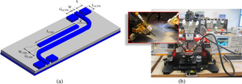
To avoid intersection between CMS electrodes and optical core, in this paper we explore concept of virtual grounding of microstrip (MS) and CMS lines to the ground pads of CPW (cf. Fig. 1(a)) by short-circuiting the bottom ground planes at RF frequencies by a capacitive coupling technique. More specifically, we propose and experimentally demonstrate an ultra-broadband via-free and low loss capacitively grounded coplanar line (CGCPW) to CMS transitions including a bent section of MS line. This transition is first realized in Rogers 3003 substrate with a low relative permittivity of ε r = 3 and low loss tangent of tanδ = 0.0013. Since our EO modulator applications, this transition is also realized and its performance reported in thin film benzocyclobutene (BCB) polymer with ε r = 2.77 and tanδ = 0.007. The modeling and measurement results demonstrate that it is possible to realize a basic CGCPW–CMS transition compatible with requirements that are applicable to thin EO polymer-based AOADC.
(a) Schematic of back-to-back of CGCPW–CMS–CGCPW transitions with a bent MS section to separate optical and RF input/output ports. (b) Photograph of the used measurement system.

II. OPERATION PRINCIPLE AND PERFORMANCES OF CGCPW–CMS–CGCPW TRANSITIONS
A schematic of back-to-back CGCPW–CMS–CGCPW transitions is shown in Fig. 1(a). This structure is analytically studied and experimentally demonstrated in this paper, first on the commercial Rogers 3003 substrate of 10 mils thick and then on a thin film of 20 µm thick BCB polymer, which is compatible with the EO polymer used for realization of phase modulators, intensity modulators, and optical deflectors. Advanced Design System from Agilent was used to initially estimate the different physical dimensions of CPW, MS, and CMS sections in order to obtain characteristic impedances of about 50 Ω. S-parameters have been measured using an Agilent E8364B vector network analyzer (10 MHz to –50 GHz) that is broadband calibrated using the short-open-line-thru (SOLT) calibration technique (cf. Fig. 1(b)). For the measurement of transition on the Rogers 3003 substrate, Cascade probes ACP40-AW-GSG-500 along with a calibration substrate from Cascade (AE-106-682) with pad width of 30 µm and pitch of 500 µm is employed that meets 40 GHz bandwidth. On the other hand, for the 20 µm thick BCB polymer substrate, the Cascade probes I40-A-GSG-250 are used with pad width of 12 and 250 µm pitch along with calibration substrate standards (Cascade AE-101-190) that also meets a bandwidth of 40 GHz. The Cascade probe station test system is controlled by the Wincal software. Full electromagnetic wave numerical simulations are performed using the three-dimensional (3D) finite-element method (FEM) modeling software (HFSS). Moreover, lumped port model of the CPW probes – available from the Cascade Probes datasheets – are also employed in order to achieve more accurate analytical predictions of the experimental set-up.
A) Evaluations of CGCPW–CMS–CGCPW transition on a thick substrate
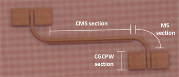
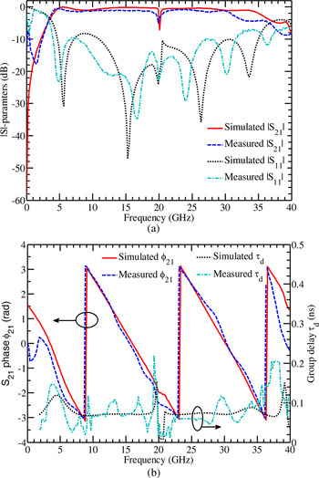
Figure 2 shows the photograph of the realized transition on the thick commercial substrate of Rogers 3003 (dielectric constant of ε r = 3, loss tangent = 0.0013). The thickness of the substrate is 10 mils and is metallized with 17 µm copper of 5 mm long CMS transmission line. The other optimized design parameters are R = 1.5 mm, S = 1.5 mm, G GCPW = 185 µm, W = 615 µm, W CMS = 150 µm, L GCPW = 1.5 mm, and G CMS = 100 µm. Figures 3(a) and 3(b) depict comparison between simulated and experimental measured S-parameters of this back-to-back circuit.
Photograph of the back-to-back CGCPW–CMS–CGCPW transition realized on Rogers 3003 substrate.

Comparison between measured and simulated characteristics of the back-to-back CGCPW–CMS–CGCPW transition on Rogers 3003 substrate: (a) Return and insertion losses of two ports circuit in dB and (b) Insertion phase and group delay from 50 MHz to 40 GHz.

A good agreement is obtained between magnitudes of the measured and simulated S-parameters, insertion phase, and group delay results over a very wide bandwidth (cf. Figs 3(a) and 3(b)). The achieved bandwidth of the back-to-back CGCPW–CMS–CGCPW transition extends from 4 GHz up to 20 GHz. The lower cut-off frequency of 4 GHz is due to the capacitive coupling limit between the coplanar ground and bottom ground plane. The group delay (cf. Fig. 3(b)) of the back-to-back CGCPW–CMS transition is also fairly flat except in the low frequency due to high-pass filter characteristics of the capacitive coupling. The insertion phase (cf. Fig. 3(b)) is almost linear resulting in minimum group delay dispersion of the RF signal, except for frequencies approaching the cut-off frequency of this capacitively grounded circuit.
B) Evaluations of CGCPW–CMS–CGCPW transition on thin BCB polymer film
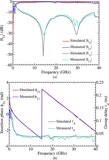
Figures 4(a) and 4(b) display simulated and measured results of this back-to-back transition realized on the BCB polymer thin film. The fabrication was done at the cleanroom of the IETR-University of Nantes using a photolithography technique with a Karl Suss MJB3 mask aligner. The polymer thickness is measured to be 20 µm using profilometric measurements and is deposited by spin-coating over a 365 µm thick silicon wafer that was previously fully coated with a copper ground plane. For the top metallization, we have used copper due to its higher conductivity (5.96 × 10⁷ S/m) than that of gold (4.10 × 10⁷ S/m) or aluminum (3.50 × 10⁷ S/m). Moreover, copper has a better adhesion to BCB polymer, so a thicker metallization can be deposited, which in turn increases the bandwidth by reducing the frequency dependent Ohmic insertion losses. The length of CMS transmission line is fixed to 5 mm. The design of this transition relies on the 50 Ohm characteristic impedance matching between the CGCPW, MS, and CMS sections and promoting a smooth conversion mode from the CPW mode to the MS mode and then from the MS mode to the CMS odd-mode (i.e. the electric field is concentrated between the top strips of the CMS line). The optimum geometric design parameters are obtained after HFSS-based iterative simulations for the given thickness of 20 µm; these values are R = 500 µm, S = 1 mm, G GCPW = 55 µm, W MS = 65 µm, W CMS = 65 µm, L GCPW = 1 mm, and G CMS = 38 µm for a copper metallization thickness of t = 1 µm. The measured and simulated results, using the extracted dielectric parameters ε r = 2.77 and tanδ = 0.007, shown in Figs 4(a) and 4(b) depict a very wide bandwidth with a good agreement between measured and simulated results for magnitudes of S-parameters, insertion phase, and group delay. The experimental bandwidth of the back-to-back CGCPW–CMS–CGCPW transition on this thin polymer exceeds 40 GHz with low cut-off frequency of 3.2 GHz. The HFSS simulation results predict a transition bandwidth of 75 GHz, even though our current measurement setup is limited to frequency of 40 GHz. The low cut-off frequency is reduced compared with that of the Rogers 3003 substrate due to a larger capacitive coupling between the coplanar ground and bottom ground plane. The insertion phase and group delay (cf. Fig. 4(b)) of the back-to-back CGCPW–CMS transitions are also fairly uniform over the band except for frequency band below 3 GHz, as the operating frequency approaches corner frequency of capacitively coupled high-pass filter. This transition suffers from no RF signal distortion except at frequencies below 3 GHz.
Measured and simulated characteristics for the back-to-back CGCPW–CMS–CGCPW transition on BCB polymer thin film: (a) Return and insertion losses of two ports circuit in dB and (b) insertion phase and group delay from 45–40 GHz.

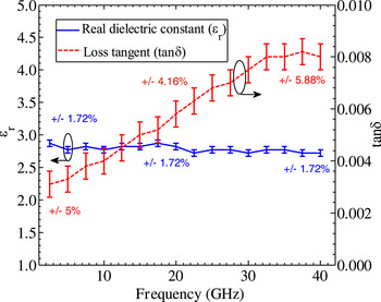
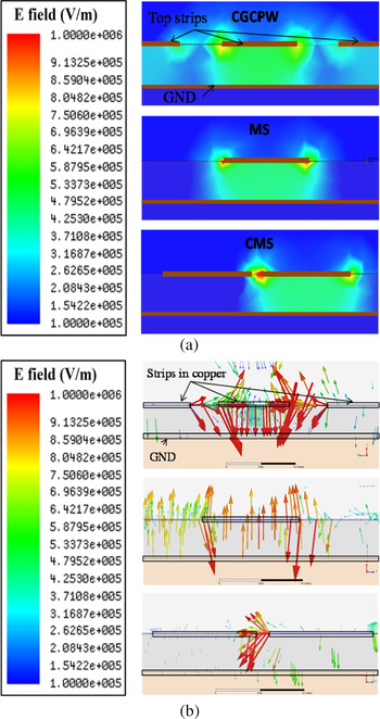
Figure 5 shows frequency dependence of the real permittivity and loss tangent of the BCB polymer over the band (1–40) GHz. These dielectric properties were extracted using a numerical fitting of scattering parameters to the measured results from a grounded CPW [Reference Hadjloum, El-Gibari, Li and Daryoush12]. Figure 6(a) shows the electric field distribution in the different sections of the CGCPW–CMS transition. At the beginning of this transition, the hybrid CPW and MS modes are converted with a pure MS mode and then from the MS mode to the even and odd CMS modes (cf. Fig. 6(b)).
Extracted complex permittivity (relative dielectric constant, ε r , and loss tangent, tanδ) of the BCB polymer as function of the frequency [Reference Hadjloum, El-Gibari, Li and Daryoush12].

Electric field in the different segments of the CGCPW, MS, and then CMS transitions at the frequency of 20 GHz and an input RF power of 4 W. High CMS field of 1 V/μm is in the region of optical waveguide. (a) Electric field distribution. (b) Electric field orientation.

III. DISCUSSIONS
The CGCPW–CMS–CGCPW structure performance depends on its physical dimensions and shape of transition for a given substrate. When one physical parameter and dimension is changed for the specific EO polymer selected for the AOADC application, the upper and lower cut-off frequencies vary often in opposite directions, as the S-parameters performances are being optimized. As the mutual coupling between the bottom and top ground planes is achieved by capacitance of a parallel plate capacitor in a thin dielectric layer, then the lower cut-off frequency of this transition is inversely proportional to this mutual capacitance, C. Then, this mutual capacitance is estimated as C = 2A·ε/h; the lower cut-off frequency of the capacitively coupled ground planes is then inversely proportional to each CPW pad surface A = S·L GCPW and the substrate permittivity ε r and is directly proportional to the substrate thickness h. Hence, the lower cut-off frequency of this capacitively coupled ground planes is reduced by increasing in the pads surface on a thin polymer thickness [Reference El-Gibari, Averty, Halbwax, Vilcot and Li11] for the given high-k dielectric substrate.
The upper cut-off for the pass-band transmission characteristics of this CGCPW–CMS transition depends on the following factors: (i) transition length, (ii) dielectric loss tangent, and (iii) resonance frequency of the coplanar microstrip mode (CPM). This mode is being excited between bottom ground plane and coplanar pads, causing energy leaking from the coplanar mode and giving rise to resonance peaks in the insertion loss (i.e. S 21 parameter). The excitation of this CPM mode causes resonance and associated variation in group delay. The dielectric material and the CMS section length are often determined by the optical deflector and modulator device performance requirements; therefore, the dimensions of these transitions are optimized to obtain the largest bandwidth.
IV. CONCLUSION
In this work, we have presented a back-to-back realization of the via-free CGCPW–CMS–CGCPW transition on Rogers 3003 substrate with a 16 GHz measured bandwidth and a low cut-off frequency of 4 GHz. The achieved bandwidth of the transition on the BCB polymer is large than 36.8 GHz with a lower cut-off frequency of about 3.2 GHz. This very large bandwidth is primarily obtained in the thin substrate thickness of 20 µm by design optimization of transition realized in low permittivity BCB polymer. Moreover, a broader transmission bandwidth is attained using high conductivity and good adhesion of copper to BCB polymer. To our best knowledge, 40 GHz-bandwidth has never been achieved for via-free CGCPW–CMS–CGCPW transitions. This reliable and simple to fabricate transition design will find applications in both optical modulators and deflectors.
ACKNOWLEDGEMENT
This work was supported by the Region of Pays de la Loire under the project ADC PolyNano (Grant number 2013-10079).
 Massinissa Hadjloum received the Engineer and Master degrees in electronics from the National Polytechnic School of Algiers, Algeria, and the National Higher Engineering School of Poitiers, France, in 2012 and 2013. He is currently working toward the Ph.D. degree with the Institute of Electronics and Telecommunications of Rennes (IETR) at the University of Nantes, France. His research interests include the areas of microwave-photonics, electro-optical modulators/deflectors and RF transmission lines. He has more than 15 scientific and technical papers.
 Dr. Mohammed El Gibari received his MS from the University of Rouen (France) in 2006 and his Ph.D. from the University of Nantes in 2009. From 2011, he is an Associate Professor at the University of Nantes. His current research interests at IETR (Institute of Electronics and Telecommunications of Rennes) include broad-bandwidth microwave photonic devices and transitions based on polymers. He has participated in several research project, MATTADOR/MILES on modulators based on electro-optic (EO) polymers (2007–2009) and ADC PolyNano (2013–2017) on analog-digital convertors based on EO polymers supported by the Region of Pays de la Loire, MODPOL (2008–2011) on high-speed modulators based on EO polymers supported by French Research Agency and the 100GRIA FUI (2010–2011) on packaged pump module with 1.2 W output power integrating the high power semiconductor diodes (550 mW) supported by French Ministry of Industry. He is author and co-author of over 35 articles and conferences.
 Hongwu Li received his BS from Beijing Institute of Technology in 1982. He obtained his Ph.D. form the University of Besançon (France), for his work on nonlinear optical self-switching devices. From 1987 to 1990, he worked on photorefractive crystals for optical image processing at the University of Angers as an assistant. He joined the National Engineering School of Brest in 1990, where he worked as an Associate Prof. until 2001 on semi-conductor (SC) optical amplifiers and lasers and acousto-optic cells for telecommunications applications. From 2001 to 2005, he worked on RF signal generation, submicron guides and optical switches as a Prof. at IEMN (Institute of Electronics, Microelectronics and Nanotechnology) of Lille University of Science and Technology. Since 2005, he is Prof. of ECE at the University of Nantes. His current research interests at IETR (Institute of Electronics and Telecommunications of Rennes) include broad-bandwidth microwave photonic devices based on polymers and radio over fiber for high-speed transmission domestic networks. He has taught a variety of courses in optics, photonic devices, information and signal theory, theory of digital communications, physics on SC components, electromagnetism, microwaves and filtering. Prof. Li has led scientific and industrial research projects with the National Research Agency, France Telecom, Thales and the European Spatial Agency. He has published over 100 scientific and technical papers.
 Afshin Samimi Daryoush received his BS (1981) from Case Western Reserve University, MS (1984), and Ph.D. (1986) from Drexel University, all degrees in Electrical Engineering. After graduation, Prof. Daryoush joined Drexel University, where he has developed courses in devices, circuits, and subsystems employed in microwaves, photonics, and antennas. He is recipient of the Drexel University’s Graduate Teaching Award in 2000 and the IEEE Philadelphia Section’s Franklin Key Award in 2015. He also conducts research in microwave photonics applied to telecommunications and biomedical engineering that resulted in over 300 technical papers, seven patents, and six book chapters. After receiving the Microwave Prize in 1986, 13 papers of Prof. Daryoush has been recognized as the best student papers in various IEEE conferences. Dr. Daryoush has also served the IEEE in various capacities, such as chair of Philadelphia joint AP/MTT chapter (1993–1995, 2014–2016), founding faculty advisor to the Graduate Student Chapter at Drexel University (2007–present), member of IEEE publications (1998–2001), and IEEE Fellow (2014) Committees. He has organized various IEEE conferences since 1993, particularly served as TPC Chair of RWS2008 and chair of the RWW2009, MWP2010, BenMAS2014, and IMS2018. He was elevated to IEEE Fellow in 1999 and became member of the Franklin Institute’s Committee on Science and the Arts in 2011.