I. INTRODUCTION
Microelectromechanical systems (MEMS) have broadened the definition of functional microsystems through integration of mechanical and electronic components within a single structure. The unique capabilities of these systems in combination with the economic advantage of high volume/low unit cost production have expanded the application of MEMS Reference Spearing1 to include devices such as sensors, Reference Esashi2 actuators, Reference Wilson, Jourdain, Zhang, Dorey, Bowen, Willander, Wahab, Al-hilli, Nur, Quandt, Johansson, Pagounis, Kohl, Matovic, Samel, van der Wijngaart, Jager, Carlsson, Djinovic, Wegener, Moldovan, Iosub, Abad, Wendlandt, Rusu and Persson3 micropower generators, Reference Weiss4 chemical reactors, Reference Jensen5 and biomedical devices. Reference Ponmozhi, Frias, Marques and Frazao6 Continued diversification of this portfolio is widely anticipated, but predicated on concomitant development of appropriate materials, fabrication technologies, and modeling approaches.
History has shown that MEMS-based devices are becoming more complex. Decades ago, the industry witnessed inkjet print heads, a silicon-based MEMS device with no moving parts containing a heating element and an orifice, transform document printing. In subsequent decades, silicon-based devices became more complex and included moving components that enabled the creation and commercialization of pressure sensors, accelerometers, and gyros. Through miniaturization, improved sensor design and controls, and volume fabrication MEMS-based sensors have made their way into consumer-based products where the sensor is valued for its ability to monitor and control. An emerging opportunity for the miniaturization of sensors and MEMS exists from industrial process controls to the monitoring of residential and commercial spaces as described by the concept of the “Internet of Things”. Reference Ashton7 Taking sensors into the often harsh environments (temperatures greater than 200 °C, power levels above 100 W) will require new approaches to MEMS devices and that often begins with identifying the materials to construct these sensors from.
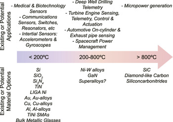
To date, material selection for the structural element of many MEMS devices is limited to a relatively small subset of materials compatible with conventional very-large scale integration fabrication technologies—see Fig. 1, with silicon being the dominant structural material. Suspended silicon or polysilicon elements can be found in most accelerometers and are fabricated through deep reactive ion etching (DRIE) of single-crystalline silicon. Thin film vapor-phase deposited materials like silicon nitride are often used to form thin membranes used for pressure sensors and thermopiles. Other vapor phase deposited materials, though less common, have been used as structural materials including but not limited to SiGe; Reference Witvrouw8 pure aluminum, copper, gold, and platinum; and silicon carbide, silicon oxide, silicon nitride, and titanium nitride. Reference Wilson, Jourdain, Zhang, Dorey, Bowen, Willander, Wahab, Al-hilli, Nur, Quandt, Johansson, Pagounis, Kohl, Matovic, Samel, van der Wijngaart, Jager, Carlsson, Djinovic, Wegener, Moldovan, Iosub, Abad, Wendlandt, Rusu and Persson3 Alternatively, components can be molded through electrodeposition techniques such as Lithographie Galvanisierung Abformung (LIGA), which is capable of fabricating high-aspect ratio nickel structures appropriate for load bearing roles. Reference Buchheit, LaVan, Michael, Christenson and Leith9,Reference Cho, Hemker, Lian, Goettert and Dirras10
Examples of existing and potential MEMS materials with respect to different applications and operating regimes.

Despite the ability to create precise and highly complex geometries, the limited range of material properties currently accessible is insufficient for many next generation applications, especially those subject to elevated temperatures. These applications will not only require operation in a harsher environment but will also require MEMS devices that can sustain movement, including surfaces that contact and wear. For example, power MEMS, such as microturbines or miniature internal combustion engines, are regarded as a highly promising frontier in the MEMS community. Reference Jacobson and Epstein11,Reference Chou, Yang, Chua, Li and Zhang12 Several examples have been successfully developed; however, these prototypes are severely limited in their capacity and efficiency due to material deficiencies in high temperature mechanical integrity and surface wear. Reference Epstein13,Reference Liamini, Shahriar, Vengallatore and Fréchette14 Power MEMS have received a considerable amount of attention in the last decade, but even greater potential for expansion of the field exists at more intermediate temperatures (200–800 °C) as illustrated in Fig. 1. Reference Neudeck, Okojie and Liang-Yu15 Unfortunately, there are fewer economical material choices in this temperature range that exhibit the combination of thermal resistance, creep resistance, mechanical integrity, and wear that will be required for the future sensors.
This has prompted renewed interest in exploring a broader range of structural materials for intermediate and high temperature MEMS applications and has illuminated the challenges associated with integrating new materials into such a highly refined process. In particular, well-defined material properties of materials that can be fabricated and shaped on the microscale and used at elevated temperatures are needed. Reliable definition of such properties is a formidable challenge and further refinement of micromechanical characterization techniques is ongoing. Reference Hemker and Sharpe16 This review was written to highlight emerging materials suitable for elevated temperature MEMSs from the perspective of processing and characterization efforts. Si-based devices are introduced first to provide a baseline for properties, processing routes, and challenges. The following section covers other Si-based material systems that are already in use or under development such as silicon carbide (SiC) and silicon carbonitrides (SiCN). The final section focuses on Ni-based systems including the popular LIGA Ni, efforts to modify pure nickel via vapor phase routes as well as more complex chemistries ranging from Ni–W to conventional Ni-based superalloys.
II. Si-BASED DEVICES
At the core of Si-based MEMS are the well-documented electronic and mechanical properties of single-crystalline and polycrystalline silicon (polysilicon). Integrated circuit (IC) foundries provide access to two key processing routes—surface and bulk micromachining—that have played an important role in the development of Si-based MEMS. Reference Madou17,Reference Wise18 An attractive aspect of silicon as a mechanical MEMS material is the cross wafer uniformity of its properties and its reproducibility that leads to a level of predictability. Even within these sophisticated fabrication approaches, there remain some challenges specific to MEMS development. Surface micromachining is often limited to a depth of several micrometers, which is insufficient for delivery of compressive or bending mechanical loads or to define the necessary channels or voids necessary for fluidic chemical or biological applications. This can be addressed through bulk micromachining; however, the deep etching process may result in undercutting or preferential etching and ultimately limits the aspect ratio of certain features. Progress towards higher aspect ratios through techniques like DRIE or UV-photolithography is on going. Reference Jensen, Yalçinkaya, Jacobsen, Rasmussen, Rasmussen and Hansen19–Reference Wu, Kumar and Pamarthy21 Developing the correct combination of materials, etchants and etch stops must be considered for new configurations and are especially important when introducing unconventional complementary metal oxide semiconductor (CMOS) materials. Regardless of these drawbacks, Si-based fabrication methods represent the most complete and well-understood toolset for MEMS development.
Mechanical characterization of single-crystalline and polycrystalline-Si has been the subject of numerous studies; many of the results have been compiled by Sharpe. Reference Hemker and Sharpe16,Reference Sharpe22 A wide range of values for the elastic modulus was initially published for both materials, but with time both experimental measurements and numerical predictions have converged on a Young's modulus of between 160 and 166 GPa for randomly oriented and <110> textured polysilicon. Reference Sharpe, Bin, Vaidyanathan and Edwards23,Reference Jayaraman, Edwards and Hemker24 The Young's modulus of single-crystalline Si is a function of orientation and can be predicted from single crystal anisotropic elastic constants. The fracture strength is less well characterized, largely because brittle failure is dependent on flaw size and distribution, which has been shown to vary significantly with mask resolution and processing conditions Reference DelRio, Friedman, Gaither, Osborn and Cook25 as well as specimen size and geometry. Reference Hemker and Sharpe16 Values between 1.0 and 3.0 GPa are generally accepted. Reference Sharpe22
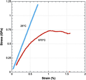
For many applications, room temperature evaluation is not sufficient. For example, some sensors and actuators for automotive applications may be subjected to temperatures up to 140 °C Reference Müller-Fiedler and Knoblauch26 and other devices that are thermally activated may experience temperatures up to 500 °C. Nakao et al. applied an on-chip tensile testing method on a heated stage to examine the high temperature mechanical properties of single-crystalline Si thin films. Reference Nakao, Ando, Shikida and Satol27 The Young's modulus was found to only decrease slightly, but significant changes in the fracture stress were observed above 400 °C with associated evidence of plasticity. The fracture stress at 500 °C was only 32% of that measured at room temperature. Inelastic behavior was also observed by Sharpe at 670 °C, Fig. 2, in this case using resistive heating. Reference Sharpe, Dulieu-Barton and Quinn28 This severe thermal degradation is expected to limit the use of Si in many thermally harsh environments envisioned for future MEMS applications. Furthermore, while fatigue is not generally expected to occur in silicon at room temperature under operating stresses of 2 GPa, Reference Ando, Shikida and Sato29,Reference Muhlstein, Howe and Ritchie30 it has been reported in polysilicon Reference Alsem, Pierron, Stach, Muhlstein and Ritchie31–Reference Kahn, Ballarini and Heuer33 and may be further accelerated under more aggressive chemical or thermal environments. Reference Romig, Dugger and McWhorter34
Stress–strain curves for a polysilicon microtensile sample. Adapted from Ref. Reference Sharpe121.

III. OTHER Si-BASED MATERIAL SYSTEMS
Several other Si-based materials are commonly found in conventional MEMS. Moreover, ceramics such as silicon dioxide (SiO2) and silicon nitride (Si3N4) are easily deposited and inherent to many IC processes. SiO2 films are often used as sacrificial layers in the micromachining process as they are easily dissolved in etchants that do not attack polysilicon. SiO2 may also be used as an etch mask for dry etching of polysilicon. Reference Zorman and Mehregany35 While serving several purposes in the fabrication of complex MEMS, SiO2 is rarely used as a structural component due to both reduced stiffness (73 GPa) and fracture strength (1 GPa) when compared with polysilicon. Reference Spearing1 The stiffness of silicon nitride (∼250 GPa) is on par or a little higher than that of polysilicon, with a slightly higher fracture strength (6 GPa). Reference Sharpe36 However, stoichiometric Si3N4 thin films are prone to high residual stresses, which limit the thickness to a few hundred nanometers. Si-rich nonstoichiometric silicon nitride films can also be deposited via low pressure chemical vapor deposition (LPCVD) to successfully reduce the residual stresses, but the mechanical performance suffers. Reference Zorman and Mehregany35 As a result, the use of Si3N4 remains somewhat limited to membranes and resonators as well as for its thin film properties of electrical isolation and surface passivation.
SiO2 and Si3N4 are part of the conventional IC materials set; however, there are several other Si-based materials that are becoming more common in MEMS applications based on processing advantages or their superior mechanical properties and thermal stability. SiGe-based MEMS have generated considerable interest because the processing temperature can be limited to below 450 °C, Reference Witvrouw8 enabling direct integration with CMOS and even polymer substrates in some cases. Reference El-Rifai, Sedky, Van Hoof, Severi, Lin, Sangameswaran, Puers, Van Hoof and Witvrouw37 CMOS-MEMS integration has many important advantages including noise reduction, improved precision, and even new device applications; however, these are limited typically to the operational temperatures of CMOS of <150 °C. Conversely, silicon carbide (SiC) and polymer-derived silicon carbonitride (Si–C–N) ceramics are two of the most promising Si-based material systems with the potential for elevated temperature operation.
A. SiC
High specific strength and thermal stability make SiC an exciting candidate for high temperature MEMS. Reference Sarro38 Although the fracture strength remains highly dependent on the test configuration and specimen geometry and size, high temperature tensile tests (∼1000 °C) have shown that the strength is maintained when compared with room temperature evaluation in the same configuration. Reference Sharpe, Beheim, Nemeth, Evans and Jadaan39 A recent computational study by Wang et al. has begun to elucidate some of the fracture mechanisms specific to SiC both at ambient and elevated temperatures, including permanent deformation via bond breaking according to resolved shear stresses on an active slip plane. Reference Wang, Niu, Zhang and Lin40 The wear resistance is also exceptional, Reference Mehregany and Zorman41 enabling SiC as a viable coating material for surfaces that contact and wear. The Young's modulus of SiC can range from 300 to 700 GPa depending on the polymorph and crystallographic orientation. Reference Zorman and Mehregany35,Reference Jackson42 Hundreds of polymorphs, or polytypes—identical planar arrangement of Si and C but different stacking sequences—have been reported for SiC, but only three crystalline types exist: cubic, hexagonal, and rhombohedral. Reference Mehregany, Zorman, Rajan and Wu43 The only cubic polytype is commonly referred to as 3C-SiC (historically β-SiC). Common hexagonal polytypes are 6H-SiC and 4H-SiC. To date, bulk crystal growth of 3C-SiC is challenging and thus limiting its adaption for electronic devices and sensors. 6H-SiC and 4H-SiC can be fabricated in bulk and small wafers (<100 mm) are available; however, these remain expensive. Reference Zorman and Parro44 Homoepitaxy of 6H-SiC on single crystalline wafers is possible, but the more common approach is through heteroepitaxy of 3C-SiC on Si wafers. Polycrystalline SiC (poly-SiC) offers greater flexibility and may be deposited on a wide variety of substrates, including sacrificial SiO2. The processing temperatures for poly-SiC are also considerably lower, between 200 and 1000 °C as compared with that between 1500 and 1700 °C for deposition of the crystalline polytypes. Reference Mehregany and Zorman41 Furthermore, the texture of poly-SiC can be controlled by controlling the texture of the polysilicon substrate. It has been shown in polysilicon that texture influences important properties such as elastic modulus and thermal conductivity. This is also true for poly-SiC and careful control of crystallographic texture will be required to tailor the performance of a given thin film. Reference Mehregany and Zorman41
Yet SiC is relatively immature when compared with micromachined silicon and LIGA nickel. Several recent reviews have outlined progress in SiC MEMS, but considerable work remains necessary to realize a larger market share beyond current niche applications including high temperature micromechanical resonators in communication transceivers, pressure sensors in the oil industry, and accelerometers in airplane engines or spacecraft. Reference Sarro38,Reference Zorman and Parro44,Reference Jiang and Cheung45 Many of these challenges revolve around improving fabrication routes. Chemical vapor deposition (CVD) is used almost exclusively for SiC thin film growth, although several variations exist that are specific to the polytype or application. Atmospheric pressure chemical vapor deposition (APCVD) was one of the first techniques developed for SiC and is still routinely used for both epitaxial and polycrystalline 3C-SiC. Reference Zorman and Parro44 Large residual stresses often result from this high temperature process, usually between 1200 and 1360 °C. LPCVD results in a slower growth rate, but can more easily accommodate the thermal stresses in the thin films. Reference Jiang and Cheung45 Growth of homoepitaxial 6H-SiC or 4H-SiC must be done at very high temperatures between 1500 and 1650 °C, which limits integration into CMOS devices. Reference Zorman and Parro44 However, lower temperature (800–1000 °C) LPCVD processes have been developed for polycrystalline 3C-SiC films. Reference Stoldt, Carraro, Ashurst, Gao, Howe and Maboudian46 Plasma enhanced CVD (PECVD) allows for deposition of amorphous SiC films at substantially lower temperatures (200–400 °C). Reference Avram, Avram, Bragaru, Bangtao, Poenar and Iliescu47 Amorphous SiC (a-SiC) films can be crystallized by post-deposition annealing, but are commonly deposited as a coating material for various MEMS components. Residual stresses in a-SiC must be carefully controlled through adjustment of deposition parameters and post-deposition annealing. Reference Zorman and Parro44
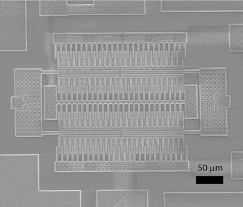
CVD is generally compatible with masking schemes to develop patterned depositions. Unfortunately, due to the chemical inertness of SiC—which for other practical purposes is desirable—typical anisotropic etchants are not effective for traditional surface or bulk micromachining. Freestanding or partially released components, such as diaphragms and cantilevers, can be fabricated through deposition on sacrificial substrates that can be bulk micromachined. Surface micromachining can be achieved in some cases when plasma-based dry etching is used, for example, see Fig. 3. Fluorine-based gas mixtures are key to the process, which can be slow and lead to anisotropic etch profiles. Reference Jiang and Cheung45 Other processes such as photoelectrochemical etching Reference Zhao, Islam and Huang48 and DRIE have also been developed for improved dimensional control and greater aspect ratios. Reference Hossain, MacLaren, Engel, Liu, Adesida and Okojie49 The latter is more commonly applied to Si, which is used as a sacrificial mold for deposited poly-SiC. Reference Zorman and Parro44 In an early example of this technique, Rajan et al. fabricated a fuel atomizer for gas turbine applications. Reference Rajan, Mehregany, Zorman, Stefanescu and Kicher50 Other micromolding techniques using preceramic polymers, such as polycarbosilane, have been developed to create high aspect ratio MEMS components. Slip casting the preceramic in a SU-8 mold followed by pyrolysis and repeated infiltration of the polymer precursor (known as the polymer infiltration and pyrolysis (PIP) process) is necessary to achieve acceptable densities. Reference Yoon, Lee, Yan and Kim51,Reference Ishikawa, Namazu, Yoshiki, Inoue and Hasegawa52 Micromolding is gaining popularity, but is not without its drawbacks as will be discussed in more detail in the following section.
A balanced-mass double-ended tuning fork fabricated from 3C-SiC deposited on a silicon substrate and shaped via surface micromachining routes. Courtesy of Azevedo et al. Reference Azevedo, Jones, Jog, Jamshidi, Myers, Li, Xiao-An, Mehregany, Wijesundara and Pisano122

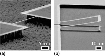
SEM images of resonant beams fabricated from AlN in a (a) nanoresonator and (b) “U” shaped configuration. Reference Förster, Cimalla, Lebedev, Pezoldt, Brueckner, Stephan, Hein, Aperathitis and Ambacher123

Challenges remain for SiC in MEMS devices, but the technology is making great strides in becoming more commercially viable. One burgeoning area involves integration of SiC and group III nitrides, such as GaN or AlN. Reference Wilson, Jourdain, Zhang, Dorey, Bowen, Willander, Wahab, Al-hilli, Nur, Quandt, Johansson, Pagounis, Kohl, Matovic, Samel, van der Wijngaart, Jager, Carlsson, Djinovic, Wegener, Moldovan, Iosub, Abad, Wendlandt, Rusu and Persson3,Reference Cimalla, Pezoldt and Ambacher53 These nitrides offer an exciting array of functionality while maintaining chemical inertness and thermal stability. This coupling may represent a whole new subset of harsh environment MEMS with further processing refinements. While a significant effort has focused on the use of these wide-band gap semiconductors as biological or chemical gas sensors, Reference Pearton, Ren, Wang, Chu, Chen, Chang, Lim, Lin and Norton54 several devices ranging from simple cantilevers Reference Davies, Huang, Gass, Papworth, Joyce and Chalker55 to micromirror arrays, Reference Wang, Sasaki, Wu, Hu and Hane56 resonating strain sensors (e.g., Fig. 4), Reference Goericke, Chan, Vigevani, Izyumin, Boser and Pisano57 and gyroscopes Reference Goericke, Vigevani, Izyumin, Boser and Pisano58 have been demonstrated. Pearton et al. Reference Pearton, Kang, Suku, Ren, Gila, Abernathy, Jenshan and Chu59 provide a more detailed discussion of the available processing routes, functional advantages, and specific device performance.
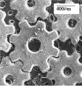
Example SiCN gear structure approximately 50 µm thick fabricated using microforged molds. Reference Liu, Liew, Luo, An, Dunn, Bright, Daily and Raj71

Finally, while many of the properties of SiC have been trumpeted as ideal for high temperature MEMS, the specific application is still very important. Take the relatively high thermal conductivity (320–490 W/m K) as an example. This is ideal for rapid heat transport but more problematic when thermal isolation is key to microsystem efficiency. In a recent report by Liamini et al. detailing the design methodology for a Rankine microturbine, Si and SiC were all but ruled out from the material selection due to the inability to sustain large thermal gradients (∼100 °C/mm) despite relatively mature manufacturing technologies. Reference Liamini, Shahriar, Vengallatore and Fréchette14 This is only one example of the trade offs between material properties and manufacturability and emphasizes that a single material system is unlikely to meet all of the needs of the many foreseeable high temperature MEMS applications.
B. SiCN
Much like SiC, silicon carbonitrides (SiCN) combine several desirable properties for high temperature MEMSs including thermal stability, high stiffness, creep resistance, and oxidation resistance. Reference Liew, Zhang, An, Shah, Luo, Liu, Cross, Dunn, Bright, Daily, Raj and Anseth60,Reference Colombo, Mera, Riedel and Soraru61 This is true for many ceramic systems; however, SiCN has the advantage of fabrication through preceramic polymers such as polyorganosilazanes. Polymer-derived ceramics (PDCs) were developed in the 1960s and 70s Reference Bill and Aldinger62 but were largely brought to the attention of the MEMS community by Liew et al. in the early 2000s. Reference Liew, Zhang, An, Shah, Luo, Liu, Cross, Dunn, Bright, Daily, Raj and Anseth60,Reference Liew, Liu, Luo, Cross, An, Bright, Dunn, Daily and Raj63,Reference Liew, Zhang, Bright, An, Dunn and Raj64
The ability to fabricate high aspect ratio components is one of the many advantages of PDCs—see Fig. 5. This includes methods to bond components together resulting in a monolithic structure. Reference Liew, Zhang, Bright, An, Dunn and Raj64 However, the properties of a PDC MEMS component are strongly influenced by the processing conditions, e.g., low density or large flaw size distribution can dramatically reduce the strength. Many processing routes have been proposed to maintain the required high aspect ratios without sacrificing reliability and mechanical integrity. These methods must also conform to common MEMS processes. Liew et al. originally proposed the use of UV-photolithographic techniques and traditional SU-8 mold to fabricate dense near-net shape components. Reference Liew, Zhang, Bright, An, Dunn and Raj64 To effectively fill the molds, the preceramic polymers must have a relatively low viscosity, which is often achieved through low solids loading. Unfortunately, such low solids content results in shrinkage of up to 30%. This large degree of shrinkage must be accounted for in the component design, but more importantly during the drying, cross-linking, and pyrolysis steps interactions between the shrinking preceramic polymer and the mold walls or substrate can lead to the build up of stress and result in microcracking or delamination. In some cases, structures with a diameter <50 µm and thinner than 20 µm can be pyrolyzed on the substrate without damage. Reference Schulz, Börner, Göttert, Hanemann, Haußelt and Motz65 Liew et al. Reference Liew, Liu, Luo, Cross, An, Bright, Dunn, Daily and Raj63 and Schulz Reference Schulz66 present a more comprehensive overview of the microcasting process advantages and challenges.
Several methods have been developed to reduce damage due to shrinkage. Use of different ceramic powder filler materials is one common route. Active filler materials (B, Si, Al, Ti, Mo, etc.) can react with the polymer decomposition products to form new phases. The resulting volume expansion effectively counteracts shrinkage and leads to near-net-shape ceramic components. Reference Greil67,Reference Greil68 If the filler material is chosen carefully, this may also improve properties such as electrical conductivity. Reference Bright, Raj, Dunn and Daily69,Reference Jung, Seo, Lombardo, Feng, Chen and Zhang70 However, changes in the scattering/absorption behavior must be accounted for in direct lithography processes when using filler materials. Reference Schulz66 A microforging process, which removes the green-body from the mold prior to drying and pyrolysis, was proposed by Liu et al. Reference Liu, Liew, Luo, An, Dunn, Bright, Daily and Raj71 In this method, the components are microcast on a NaCl substrate, the mold is removed and a sacrificial wax handling plate is used to transfer the components to the heat treatment processes, during which the wax melts away and freestanding components are left. At this point, the freestanding components must be manually placed within the MEMS device. This is a nontrivial task that may lead to warping and will greatly increase cost by eliminating massively parallel processing. Bright et al. pursued a similar route using hot isostatic pressing. Reference Bright, Raj, Dunn and Daily69 Soft lithography methods, Reference Zhang, Su and Button72,Reference Lee, Park, Hong and Kim73 PECVD, Reference Probst, Hoche, Zhou, Hauser, Stelzner, Scheerer, Broszeit, Berger, Riedel, Stafast and Koke74 and even sputtering Reference Ma, Xu, Wu, Wang, Ma, Ma, Xu and Bell75,Reference Bhattacharyya and Mishra76 have also been explored, but these ultimately limit the potential aspect ratio.
To date, most PDC work on high temperature MEMSs has focused on commercially available forms of Si–C–N precursors. The motivation for this is clear—any new processes must be economically viable and competitive with other mature MEMS processing routes. However, many other precursor-derived ceramic systems have been studied and shown to have promising mechanical properties. Reference Colombo, Mera, Riedel and Soraru61 A potentially large design space for tailoring specific properties exists if some of the aforementioned processing challenges can be overcome.
IV. Ni-BASED MATERIAL SYSTEMS
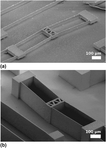
MEMS structures must be mechanically robust. To-date, MEMS designers have relied on the fact that IC-based MEMS fabrication processes significantly mitigate the introduction of critical flaws that would be detrimental to intrinsically brittle materials like the previously discussed Si-based materials. Reference Hemker and Sharpe16 By contrast, the intrinsic strength and toughness of metallic alloys are dramatically higher and can easily be tailored. The push for MEMS materials that can be reliably implemented in extreme environments and at elevated temperatures calls for the reexamination and development of metallic alloys that possess a broad range of tailorable properties and can be fabricated and shaped on the microscale. Silicon has succeeded in creating classes of two-dimensional sensors, such as accelerometers and gyroscopes, through precise thin film polysilicon deposition and processing. However, polysilicon is limited by its deposited film stress to a thickness of a few tens of micrometers in a single layer or 2–3 integrated thin layers. The connectivity of industrial systems will drive future generations of MEMS sensors and actuators that will operate at temperatures >150 °C, will require 10x improvements in sensitivity as well as stability and drift minimization. New structural materials such as metal alloys are poised to meet these sensor demands through both material properties as well as processing techniques that can enable three-dimensional MEMS sensors and high aspect ratio features—e.g., through use of carbon nanotube (CNT) scaffolding as demonstrated by Hutchison et al. in Fig. 6. Reference Hutchison, Morrill, Aten, Turner, Jensen, Howell, Vanfleet and Davis77 The integration of metals and alloys into MEMS structures would also provide a much wider design space with regard to density, electrical and thermal conductivity, and even reflectance.
An example of a high aspect ratio 3D structure fabricated from a CNT-silicon nitride composite process. (a) released bistable mechanism (BSM); (b) unreleased CNT-silicon nitride composite BSM. Courtesy of Hutchison et al. Reference Hutchison, Morrill, Aten, Turner, Jensen, Howell, Vanfleet and Davis77

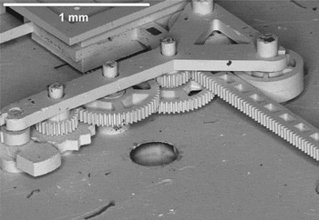
An example LIGA Ni microsystem. Reference Buchheit, LaVan, Michael, Christenson and Leith9

The wide-spread use of electrodeposited Ni in LIGA micromolding and microstructure applications and the development of multicomponent Ni-based superalloys as elevated temperature macroscale structural materials make Ni-based materials an obvious starting point for high temperature MEMS applications. The overarching challenge is to develop processing routes that allow for both microscale shaping and the development of complex alloys and material microstructures.
A. LIGA Ni
Development of the LIGA technique over the last several decades has enabled microfabrication of complex structural elements and molds that are relatively thick yet capable of maintaining a high aspect ratio—see Fig. 7. Reference Malek and Saile78 Ni is very easily electrodeposited and LIGA Ni components have received considerable attention. When the grain size is properly controlled to a nanometer scale (e.g., <100 nm Reference Ebrahimi, Bourne, Kelly and Matthews79 ) and texture accounted for, Reference Hemker and Last80 the strength of electroplated Ni increases dramatically over that of the bulk metal. In addition to being highly sensitive to the exact deposition conditions, Reference Buchheit, LaVan, Michael, Christenson and Leith9 the thermal stability of such a fine-grained, nonequilibrium microstructure is unfortunately low. Rapid softening has been observed during both annealing Reference Hemker and Last80 and elevated temperature loading. Reference Cho, Hemker, Lian, Goettert and Dirras10 Significant creep has also been observed at room temperature. Reference Collins, Wright and Muhlstein81 This instability has been attributed to the mobility of high energy grain boundaries formed through electrodeposition, and it has been suggested that if properly conditioned through cyclic loading, the grain boundaries may relax without significant grain coarsening and loss of mechanical strength at ambient temperature. Reference Collins, Wright and Muhlstein81,Reference Rupert and Schuh82 However, the application of nominally pure LIGA nickel in load bearing configurations is expected to be quite limited on the basis that most conventional MEMS packaging processes use temperature excursions beyond the threshold for microstructural stability.
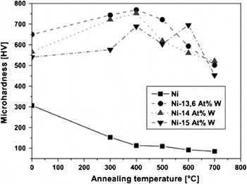
Comparison of microhardness data for LIGA Ni and several LIGA Ni–W alloys after a 2 h anneal at elevated temperature. Reference Suresha, Haj-Taieb, Bade, Aktaa and Hemker92 Reprinted with permission.

B. Binary Ni alloys
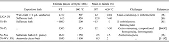
Considerable effort has been made to improve the thermal stability of the nanograin structure of electrodeposited nickel films. One promising route is through the introduction of alloying elements, such as iron, Reference Christenson, Buchheit, Schmale and Bourcier83 tungsten, Reference Yamasaki84 cobalt, Reference Buchheit, Glass, Sullivan, Mani, Lavan, Friedmann and Janek85,Reference Goods, Kelly and Yang86 or manganese. Reference Goods, Kelly and Yang86–Reference Talin, Marquis, Goods, Kelly and Miller89 Table I summarizes the mechanical properties of several binary Ni-alloys in comparison with pure LIGA Ni. Reference Buchheit, Glass, Sullivan, Mani, Lavan, Friedmann and Janek85,Reference Goods, Kelly and Yang86,Reference Hibbard, Aust and Erb90–Reference Suresha, Haj-Taieb, Bade, Aktaa and Hemker92 The as-deposited strengths are quite good; however, challenges with sulfur grain boundary segregation and grain coarsening limit the utility of the Ni–Fe Reference Buchheit, Glass, Sullivan, Mani, Lavan, Friedmann and Janek85 and Ni–Co Reference Goods, Kelly and Yang86,Reference Hibbard, Aust and Erb90 systems at elevated temperatures. While Ni–Mn performs well even after thermal annealing, maintaining a significant fraction of the as-deposited strength and a very respectable ductility, Reference Goods, Kelly and Yang86 the magnetic properties and lower density of this alloy have limited its implementation. This leaves the Ni–W system, which has somewhat limited ductility in the as-deposited condition Reference Haseeb and Bade93 but has excellent thermal stability and high density. Reference Haj-Taieb, Haseeb, Caulfield, Bade, Aktaa and Hemker91,Reference Suresha, Haj-Taieb, Bade, Aktaa and Hemker92
Comparison of the mechanical properties of several Ni-binary alloys to pure LIGA Ni.

a Data collected after 1 h anneal at 500 °C.
Originally considered for coating applications due to its superior corrosion and wear resistance, Reference Shacham-Diamand and Sverdlov94–Reference Schuh, Nieh and Iwasaki96 electrodeposited nanocrystalline Ni–W is a promising candidate for structural elements in MEMS. Reference Haj-Taieb, Haseeb, Caulfield, Bade, Aktaa and Hemker91,Reference Suresha, Haj-Taieb, Bade, Aktaa and Hemker92,Reference Keimel, Aimi, Bansal, Corderman, Kishore, Reddy, Saha, Subramanian, Thakre and Corwin97 Figure 8, from Haj-Taieb et al., Reference Haj-Taieb, Haseeb, Caulfield, Bade, Aktaa and Hemker91 illustrates the improvement in mechanical performance at elevated temperatures. The strength of LIGA Ni was largely attributed to the fine grain size achievable through electrodeposition. Reference Ebrahimi, Bourne, Kelly and Matthews79 However, this behavior has been shown to peak at some critical grain size. Schuh, Nieh, and Iwasaki Reference Schuh, Nieh and Iwasaki96 demonstrated that such a breakdown in strengthening behavior may be due to a diffusive mechanism in which case, the addition of alloying elements with limited diffusivity—such as W in Ni—would suppress this critical grain size and further increase the strength. Although the traditional (e.g., Fleischer model Reference Fleischer98 ) calculated solid solution strengthening contribution of W in Ni is quite low, the same group later presented a new strengthening mechanism based on dislocation pinning at grain boundaries. Reference Rupert, Trenkle and Schuh99 The efficiency of this mechanism is dependent on the global properties of a material including shear modulus and Burgers vector, both of which may be significantly impacted by the addition of solute atoms like W. Furthermore, subtle grain boundary segregation of W also contributes to the stability of the fine microstructures necessary for this nanocrystalline strengthening mechanism to dominate. Reference Detor, Miller and Schuh100 The added microstructural stability of subtle grain boundary solute segregation is ultimately limited to temperatures below 500 °C where normal grain coarsening ensues Reference Detor and Schuh101 and due to the onset of ordering (to Ni4W-phases) as 700 °C is approached. Reference Choi, Al-Kassab, Gärtner, Kreye and Kirchheim95,Reference Borgia, Scharowsky, Furrer, Solenthaler and Spolenak102
Other schemes including the inclusion of WO4 particles in electrodeposited Ni films Reference Miyamoto, Takehara, Uenoya, Fujiwara and Goto103 and the addition of P Reference Balaraju, Manikandanath and William Grips104 or Fe Reference He, Yang, Lei and Gu105 to electrodeposited Ni–W alloys have also been explored in the context of wear- and corrosion-resistant coatings and have not been investigated as freestanding films.
C. Vapor phase aluminization of LIGA Ni structures
Electrodeposition is easily adaptable to conventional microfabrication methods but significantly limits compositional flexibility to one or two component alloys and the deposition parameters must be carefully tailored for each new composition. Moreover, certain elements such as aluminum cannot be electrodeposited from aqueous solutions. Important classes of structural materials, e.g., nickel aluminide intermetallics and Ni-based superalloys, are excluded on this basis and alternative efforts to modify LIGA Ni with Al are required.
Vapor-phase modification of bulk Ni-based superalloys is a common approach for application of protective barrier coatings on structural components subjected to extreme environments. Development of a β-NiAl intermetallic bond coat is a typical goal of this process; however, routes for chromizing as well as siliconizing have also been developed. Reference Goward and Boone106–Reference Nicholls and Stephenson108 Pack aluminization has also been applied to much finer structures where the thickness of the deposited layer is on the same length scale as the structure itself. In these cases, an additional homogenization step results in a uniform Ni–Al alloy Reference Hodge and Dunand109,Reference Dunand, Hodge and Schuh110 or a desired two-phase γ/γ′ microstructure with the corresponding high temperature mechanical stability. Reference Johnson, Tryon and Pollock111,Reference Perez-Bergquist, Vermaak and Pollock112
Conversion of LIGA Ni MEMS components to a Ni-rich two-phase (γ–γ′) superalloy microstructure via pack aluminization has recently been explored by Burns et al. Reference Burns, Zhang, Teutsch, Bade, Aktaa and Hemker113 The aluminized components showed significantly improved microstructural stability. Furthermore, the trimodal distribution of γ′-precipitates resulted in marked improvements in both room and elevated temperature strength. These binary microsamples suffered from elevated temperature grain boundary oxidation and embrittlement, Reference Burns114 but this embrittlement can be overcome with an additional chromizing step as demonstrated by Choe and Dunand. Reference Choe and Dunand115 The full potential of nickel aluminides as structural MEMS materials appears promising, but the feasibility of a multistep homogenization process will face many of the same challenges as the silicon carbonitrides and must be assessed in the context of rapid, reliable, and compatible MEMS production.
D. Ni-based superalloys
The precipitation strengthening and oxidation resistance afforded by Al- and Cr-vapor phase modification of LIGA Ni is a first step toward approaching the high temperature mechanical performance of traditional Ni-based superalloys at the MEMS scale. Optimal performance of such Ni-based superalloys is dependent on contributions from a host of alloying elements, which cannot feasibly be incorporated via electrodeposition or pack aluminization. Sputtering provides an alternative fabrication method that has already been integrated into many MEMS processing routes and is capable of maintaining the complex compositions of a Ni-based superalloy. Sputtered binary Ni–W alloys have already been discussed and demonstrate compositional flexibility beyond equilibrium solubility levels as well as greater microstructural control. Reference Rupert, Trenkle and Schuh99,Reference Borgia, Scharowsky, Furrer, Solenthaler and Spolenak102 Nanocrystalline superalloy coatings deposited via sputtering have also been explored for corrosion Reference Liu, Li and Wang116 and oxidation protection. Reference Liu, Li and Wang116–Reference Lou, Wang, Zhu, Xia and Zhang118
Preliminary efforts to sputter first generation Ni-based superalloys in the context of freestanding films for MEMS applications have been undertaken by Burns et al. Reference Burns, Zhang, Weihs, Hemker and Huron119 As was observed for the corrosion and oxidation applications, the influence of the initial nonequilibrium microstructure of the sputtered films played an important role in dictating the properties of the thick films. The initial yield strength of the as-deposited films both at room temperature and elevated (700 °C) temperature was significantly enhanced relative to the bulk alloy. This demonstrated that the initially fine microstructure was stable even at 700 °C. However, the homogenous as-deposited films did not take advantage of the precipitation strengthening mechanism that contributes to the high temperature mechanical behavior of typical Ni-based superalloys. The conventional annealing profiles for Inconel 718 require a combination of 16 h above 600 °C. Initially, this may be seen as a hurdle for MEMS incorporation, but Burns et al. Reference Burns, Zhang, Teutsch, Bade, Aktaa and Hemker113 also demonstrated that the prevalence of grain boundaries changed the precipitation pathways in the sputtered alloy. Instead of developing the expected metastable γ″-phase, the equilibrium δ-phase was observed. This is effectively indicative of an overaged microstructure, suggesting accelerated phase evolution kinetics. Both the prevalence of heterogeneous nucleation sites, e.g., grain boundaries, and the initial stress state of Inconel 718 have previously been shown to influence the position of time–temperature–transformation (TTT) curves. Reference Oradei-Basile and Radavich120 Given that both of these variables can be tuned through the sputtering processing, this may lead to opportunities to reduce the time and temperatures necessary to develop the desired two-phase microstructure and activate precipitation strengthening in specific thin film alloys.
V. CONCLUDING REMARKS
Silicon-based MEMSs are at the core of the rapidly expanding microsystems industry. Predictable properties and streamlined fabrication methods assure that Si will continue to play an important role in the industry. However, a broader spectrum of MEMS materials would offer a wider range of functionality and fuel a greatly expanded assortment of MEMS applications especially in extreme environments. Several candidate material systems including silicon carbide (SiC), silicon carbonitrides (SiCN), and nickel-based alloys have been reviewed based on their potential for high temperature MEMS integration. SiC is the most mature of these technologies. Impressive thermal stability and wear resistance are among the attractive properties of SiC. Efforts to reduce cost and to improve control of aspect ratio and residual stress in deposited structures will further improve the feasibility of SiC. The high thermal conductivity of SiC is attractive for many applications but not all—in these cases, SiCNs are a viable alternative if component shrinkage and methods for reliable placement can be developed. Metallic systems may provide the greatest potential to tune strength and reliability of MEMS components at elevated temperature. Simple electrodeposited binary nickel alloys such as Ni–W have already demonstrated high strength and thermal stability up to 500 °C. Increasingly complex alloys provide the opportunity to improve upon high temperature corrosion and oxidation resistance, dimensional stability, and damage tolerance (cyclic and static). Processing methods such as sputtering also provide much needed flexibility to tune grain size and residual stress, which are not only important to dimensional tolerances but also offer opportunities to accelerate microstructure development necessary for optimal high temperature mechanical properties.
Each of these new MEMS materials must overcome unique challenges before successful integration. However, the driving force for continued expansion of the MEMS industry into more extreme environments is likely to provide the necessary impetus for continued development of these and future MEMS materials.