
Introduction
Printed electronics technology is expected to realize facile productions of large-area, light-weight, and flexible electronics devices without using huge vacuum facilities.[Reference Sirringhaus1,Reference Fukuda and Someya2] The most crucial target is to realize high-resolution and all-printed thin-film transistor (TFT) arrays that are applicable to the industry. Extensive studies have been dedicated for solution-processable organic semiconductors to produce channel semiconductor layers, while electrode printing techniques have been also intensively studied, almost independently, by using metal nanocolloids that are the dense suspension of ligand-encapsulated metal nanoparticles.[Reference Sekitani, Noguchi, Zschieschang, Klauk and Someya3–Reference Perinot, Kshirsagar, Malvindi, Pompa, Fiammengo and Caironi5] The further challenge is to integrate and combine these printing techniques and realize high electrical performance in their all-printed devices.
Recently, we successfully developed a groundbreaking electrode printing technique, which we call as surface photo-reactive nanometal printing (SuPR-NaP).[Reference Yamada, Fukuhara, Matsuoka, Minemawari, Tsutsumi, Fukuda, Aoshima, Arai, Makita, Kubo, Enomoto, Togashi, Kurihara and Hasegawa6] The technique is based on the chemisorption effect of silver nanoparticles on activated patterned perfluoropolymer surfaces, by taking advantage of the unique nature of specific silver nanocolloids that show self-sintering characteristics. The technique allows easy, high-speed, and large-area manufacturing of ultrafine metal wiring with a minimum line width of 800 nm, so that it is quite promising as the practical device fabrication processes. In the SuPR-NaP technique, a dense amorphous perfluoropolymer, Cytop, is used to produce the activated patterned surfaces. The Cytop is also known to useful as the gate dielectric material, because it not only shows excellent insulating characteristics but also provides a clean semiconductor/insulator interface due to the highly hydrophobic nature.[Reference Blülle, Häusermann and Batlogg7,Reference Kalb, Mathis, Haas, Stassen and Batlogg8] Thus, it is quite promising to integrate the SuPR-NaP technique, for producing source/drain printed electrodes, to realize bottom-contact and all-printed TFTs. However, the highly hydrophobic nature of Cytop surface made it difficult to utilize the solution technique for producing uniform printed semiconductor layers.
In this communication, we report that the SuPR-NaP technique can be integrated to realize printed polymer TFTs, by using the push-coating technique for producing uniform printed polymer semiconductor layer.[Reference Ikawa, Yamada, Matsui, Minemawari, Tsutsumi, Horii, Chikamatsu, Azumi, Kumai and Hasegawa9] We demonstrate that the obtained polymer TFTs, using a class of donor–acceptor (D–A)-type copolymer, PDVT-10, as the channel semiconductor material, exhibit excellent device characteristics with showing small hysteresis. We conducted the transfer length method (TLM) measurements on these devices, to disclose and discuss the contact resistance and short-channel effects.
Experimental details
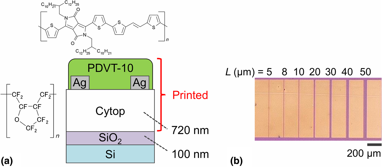
In the device fabrication, we employ bottom-gate bottom-contact geometry, as presented in Fig. 1(a). We used a highly p-doped Si substrate with a 100 nm-thick surface silica layer, which is used as the gate electrodes/gate dielectric layer. On the substrates, the Cytop layer is produced by spin coating the solution (CTL-809M; AGC Inc., Tokyo, Japan). The Cytop layer is used not only for the SuPR-NaP technique but also for the gate dielectric layer coupled with the silica layer. Here, we used a relatively thick (720 nm) Cytop layer in order to establish enough high insulating properties for all the TLM measurements. Then, we produced printed source/drain electrodes by the SuPR-NaP technique, as described in detail in Ref. [Reference Kitahara, Aoshima, Tsutsumi, Minemawari, Arai and Hasegawa10]. All the devices with a various channel length (L), including the short-channel length as small as L = 5 µm, were produced by the SuPR-NaP technique through the nanoparticle chemisorption effect. The surface of printed silver electrodes was treated chemically by pentafluorobenzenethiol (TCI Co. Ltd., Tokyo, Japan) vapor, in order to improve the carrier injection characteristics.[Reference Aoshima, Arai, Fukuhara, Yamada and Hasegawa11] A class of D–A-type copolymer, poly[2,5-bis(alkyl)pyrrolo[3,4-c]pyrrole-1,4(2H,5H)-alt-5,5′-di(thiophen-2-yl)-2,2′-(E)-2-(2-(thiophen-2-yl)vinyl)thiophene] (PDVT-10; 1-Material Inc., Dorval, Canada), was used as a semiconductor material.[Reference Chen, Guo, Yu, Zhao, Zhang, Gao, Liu and Liu12] We used a 0.1 wt% semiconductor solution in anhydrous 1,2,4-trichrolobenzene (Sigma-Aldrich Co. LLC., USA), and used the push-coating technique to produce uniform thin films.[Reference Ikawa, Yamada, Matsui, Minemawari, Tsutsumi, Horii, Chikamatsu, Azumi, Kumai and Hasegawa9] The semiconductor thin films were then thermally annealed at 80 °C for 20 min, in order to improve the crystallinity and the device characteristics. Finally, unnecessary part of the semiconductor films outside the channels was trimmed away by using micromanipulator (Axis-Pro; Systems Engineering Inc., Tokyo, Japan), in order to adjust the channel width accurately, and thus to estimate the mobility correctly by eliminating the effect of fringe current.[Reference Pei, Chen, Zhou, Li and Chan13]Figure 1(b) shows the optical micrograph of printed TFTs with a channel length ranging from 5 to 50 µm for TLM measurements. We measured the film morphology by an atomic force microscope (VN-8010; Keyence Corp., Osaka, Japan). The thickness distribution of the films is presented in Supplementary Fig. S1. All electrical measurements were carried out in the N2-filled glove box (O2 < 1 ppm).
(a) Schematic of printed TFTs. (b) Optical micrograph of printed TFTs for TLM measurements. The channel length (L) is variable (5–50 µm), and the channel width (W) is fixed at 800 µm.

Results and discussion
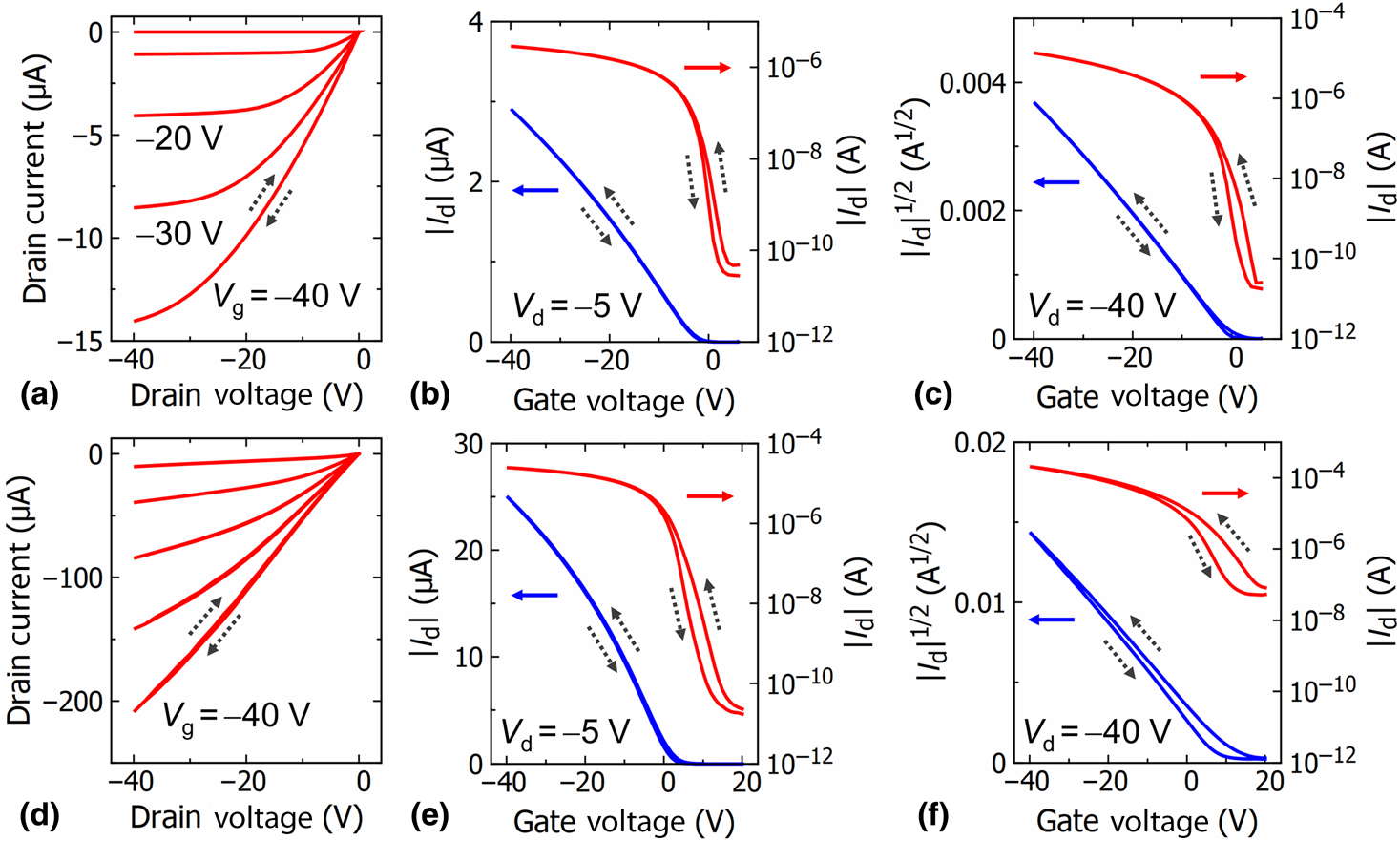
Figure 2 presents the electrical characteristics of printed TFTs with relatively long- (L = 50 µm) and short- (L = 5 µm) channel lengths. In the long-channel device, the output characteristics exhibit typical linear and saturation TFT characteristics without showing noticeable hysteresis [Fig. 2(a)]. The transfer characteristics show small hysteresis and enough large on/off ratio (106) [Figs. 2(b) and 2(c)]. In contrast, the output characteristics show deviation from the typical TFT characteristics in the short-channel device: The saturation behavior disappears, as shown in Fig. 2(d). The concomitant positive threshold voltage (V th) shift is observed in the transfer characteristics [Figs. 2(e) and 2(f)]. In the saturation regime, the switching characteristics are degraded, where both the hysteresis width and off-current are increased. We consider that the switching characteristics should be degraded due to the electron injection at the drain electrode in case of the large negative drain voltage in PDVT-10 that has relatively small bandgap (1.68 eV).[Reference Liu, Ge, Zhang, Ma, Ding, Yu and Hu14] Actually, we clearly observed the ambipolar characteristics with the positive gate bias at V d = −40 V (see Supplementary Fig. S2). We consider that the switching characteristics should be degraded due to the electron injection at the drain electrode in case of the large negative drain voltage.
Typical electrical characteristics of printed TFTs with different channel lengths (L). L = 50 µm for (a–c) and L = 5 µm for (d–f). Output characteristics (a and d), transfer characteristics in the linear regime (b and e), and in the saturation regime (c and f).

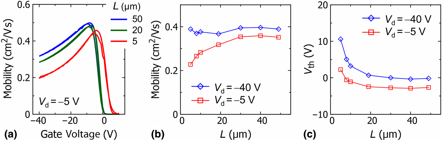
Figure 3(a) shows the mobility in the linear regime as a function of gate voltage (V g) or the first derivative of transfer characteristics with various channel lengths, calculated from the following equation:
 $$\mu = \displaystyle{L \over {WC_{\rm i}V_{\rm d}}}\left( {\displaystyle{{\partial I_{\rm d}} \over {\partial V_{\rm g}}}} \right)$$
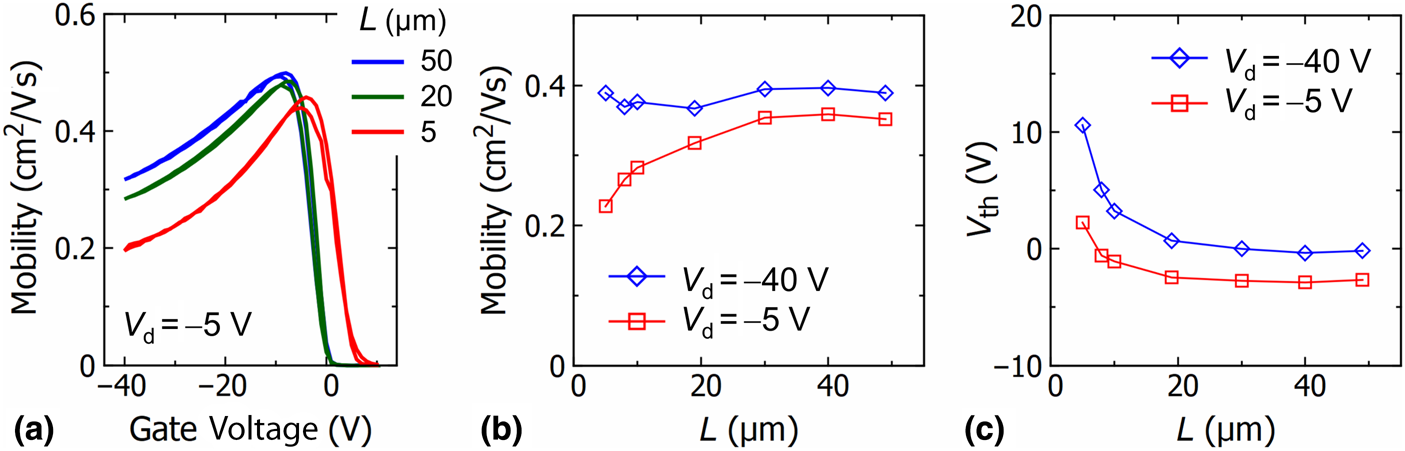
where L is the channel length, W is the channel width, C i is the areal capacitance of gate dielectric, V d is the drain voltage, and I d is the drain current. Here, we estimated the mobility as an average value between V g = −40 and −25 V. The mobility value in the linear regime (V d = −5 V) decreases as the channel length decreases [see Fig. 3(b)], which could be ascribed to the effect of contact resistance. Note that the observed peak in the V g dependence of mobility [Fig. 3(a)] should be also related to the effect of contact resistance.[Reference Uemura, Rolin, Ke, Fesenko, Genoe, Heremans and Takeya15] The estimated mobility value is comparable to those of former reports.[Reference Tsutsumi, Matsuoka, Osaka, Kumai and Hasegawa16,Reference Kwon, Yu, Kweon, Kim, Kim, Kim, Jo, Kim, Kim, Lee and Lee17] Note that the value is considerably smaller than that of the initial report[Reference Chen, Guo, Yu, Zhao, Zhang, Gao, Liu and Liu12] that might include an overestimation because of the possible electron injections at the contacts.[Reference Okachi18] In contrast, mobility does not show an apparent degradation in the saturation regime, even in the case of a short-channel device. It indicates that the contact resistance is more dominant in the linear regime than in the saturation regime because the pinch-off voltage is independent of the voltage drop at the contact and is more important in the saturation characteristics. Figure 3(c) shows the channel length dependence of V th, obtained by the extrapolation of linear fit for the initial rise of the transfer curve. The positive shift of V th is clearly observed, as the channel length decreases. The shift should originate from charge accumulation caused by a relatively strong longitudinal electric field in the short-channel devices, as is known as the roll-off effect or drain-induced barrier lowering in inorganic MOSFETs[Reference Sze19] and also in organic TFTs.[Reference Haddock, Zhang, Zheng, Zhang, Marder and Kippelen20,Reference Yokota, Sekitani, Kato, Kuribara, Zschieschang, Klauk, Yamamoto, Takimiya, Kuwabara, Ikeda and Someya21] The nonsaturation behavior as observed in the output characteristics [Fig. 2(d)] should be due to the positive V th shift as occurred during the drain voltage sweep.
Channel length dependence of device characteristics. (a) Mobility as a function of gate voltage in the linear regime with various channel lengths. (b) Estimated mobility from the transfer curve. The mobility is estimated as the average value from V g = −40 to −25 V. (c) Estimated threshold voltage (V th) from the transfer curve. The V th is obtained by the extrapolation of linear fit for the initial rise of the transfer curve.
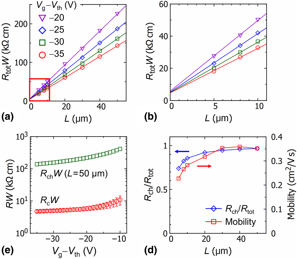
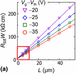
Figures 4(a) and 4(b) shows the TLM plots of width-normalized total resistance (R totW), obtained from the device resistance in the linear transfer characteristics. We used gate overdrive voltage (V g − V th) which is effective to satisfy the assumption of the TLM analysis that the channel carrier density becomes constant.[Reference Borchert, Peng, Letzkus, Burghartz, Chan, Zojer, Ludwigs and Klauk22] The reliable regression lines are successfully obtained in respective plots, which provides highly accurate estimations of channel resistance and contact resistance at each gate overdrive voltage, with all coefficients of determination (R 2) larger than 0.999. We consider that the high accuracy in TLM plots could be ascribed to the highly hydrophobic nature of Cytop gate dielectric as well as to the highly uniform nature of semiconductor films (Supplementary Fig. S1). The width-normalized contact resistance (R cW) is evaluated as 4.7 kΩ cm with gate overdrive voltage (V g − V th) at −35 V, and the channel resistance (R chW) at L = 50 µm is 1.4 × 10² kΩ cm [Fig. 4(c)]. The obtained R cW is larger than the smallest value reported for organic TFTs with evaporated source/drain electrodes (29 Ω cm by Borchert et al.[Reference Borchert, Peng, Letzkus, Burghartz, Chan, Zojer, Ludwigs and Klauk22]). Nonetheless, the achieved R cW value is much smaller compared to the typical value for the bottom-contact TFTs with printed silver electrodes,[Reference Aoshima, Arai, Fukuhara, Yamada and Hasegawa11, Reference Chung, Jeong, Kim, Park, Lee and Hong23–Reference Fukuda, Sekine, Kobayashi, Takeda, Shimizu, Yamashita, Kumaki, Itoh, Nagaoka, Toda, Saito, Kurihara, Sakamoto and Tokito25] or approximately comparable to the best value.[Reference Fukuda, Takeda, Mizukami, Kumaki and Tokito26] We also show the TLM plots for the another series of devices produced on a different substrate in Supplementary Fig. S3. We found that highly accurate TLM analysis is also obtained, though the estimated contact resistance R cW is relatively higher (12 kΩ cm). It means that the semiconductor/electrode interface should be uniformly formed at least for each substrate but depends on the subtle processing conditions. Figure 4(d) presents the channel length dependence of normalized channel resistance (R ch/R tot), with a comparison of the mobility in the linear regime [Fig. 3(b)]. These two plots are roughly consistent with each other in the short-channel devices. We consider that the normalized channel resistance (R ch/R tot) should be more accurate to determine the channel transport characteristics because the mobility estimation from the first derivative of the transfer characteristics should be ambiguous as to the V g dependence of mobility [Fig. 3(a)].
TLM analysis of printed TFTs. (a) TLM plots extracted from the device resistance in the linear (V d = −5 V) transfer characteristics. The solid line corresponds to the regression line for fitting. (b) Magnified view of TLM plots in the case of a short-channel device, shown by the red square in (a). (c) Gate overdrive voltage (V g − V th) dependence of channel resistance (R chW, shown as green square) and contact resistance (R cW, shown as red circle) with error bars showing the standard error from the regression line for each gate overdrive voltage. The estimated R cW at V g − V th = −35 V is 4.7 kΩ cm, and the R chW is 1.4 × 10² kΩ cm. (d) Channel length dependence of mobility in the linear regime (V d = −5 V) and of the normalized channel resistance (R ch/R tot).

Conclusion
We successfully integrated the SuPR-NaP technique for printing silver electrodes and the push-coating technique for fabricating uniform polymer semiconductor layer, to realize the printed polymer TFTs. With the use of PDVT-10 as the polymer semiconductor, we obtained excellent device characteristics with showing small hysteresis. Highly reliable estimations of the contact resistance with the use of the TLM plots were demonstrated in the printed polymer TFTs. The extracted contact resistance is considerably small (4.7 kΩ cm) among the organic TFTs with printed silver source/drain contacts, indicating the excellent compatibility of the SuPR-NaP technique with the polymer semiconductors. These findings pave the way for the industrial application of printed electronics technology for the productions of large-area, light-weight, and flexible electronics devices.
Supplementary material
The supplementary material for this article can be found at https://doi.org/10.1557/mrc.2019.126.
Acknowledgments
This study was supported by JST CREST (Grant No. JPMJCR18J2) and A-STEP (Grant No. VP30318087386) from the Japan Science and Technology Agency, and JSPS KAKENHI (Grant No. 18H03875) from the Japan Society for the Promotion of Science (JSPS). This study was also supported by the research grant from the Leadership Development Program for Ph.D. (LDPP) in the University of Tokyo.