





Introduction
To achieve a significant reduction in greenhouse gas emissions, industry is required not only to adopt recycled resources and renewable energies but also to improve resource efficiency in the production of energy-intensive goods such as plastic pipes, blow-molded hydrogen tanks, and sheet or foam materials. According to [1], the fabrication of 1 kg of PVC sewer pipe, corresponding to only 65 cm in length with a wall thickness of 3 mm and a diameter of 110 mm, requires 59.3 MJ of non-renewable and 14.7 MJ of renewable energy, along with 10.7 L of fresh water, while generating 2.76 kg of CO $_2$-equivalent emissions. Even minor deviations in wall thickness can render the product unusable, resulting in a waste of these resources. To mitigate this risk, inline sensors can be employed to monitor and control the wall thickness during production, maintaining the target dimensions. Frequency-modulated continuous-wave (FMCW) radar systems are widely applied in high-resolution measurements and can determine absolute distances with sub-micrometer accuracy [Reference Piotrowsky, Kueppers, Jaeschke and Pohl2]. Their range resolution, however, is limited to approx. 3 mm [Reference Hansen, Bredendiek, Briese, Froehly, Herschel and Pohl3], which is insufficient for the use case, since the majority of commonly used pipes have wall thicknesses of only a few millimeters and film materials are only several microns thick. In practice, the required resolution is obtained using ionizing radiation methods such as X-rays or beta emitters, despite the associated health risks, whereas laser-based THz systems remain costly, unreliable, and therefore limited to niche applications. Broadband pulse-based transceiver systems at THz frequencies represent a promising alternative, which could provide the resolution required for accurate thickness control, while offering a fully integrated architecture and thus a robust, cost-effective approach. A similar configuration employing additional focusing mirrors was previously demonstrated in [Reference Razavian and Babakhani4] for transmission-based imaging.
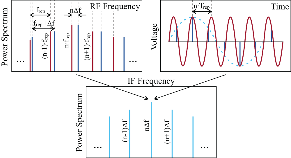
The proposed system relies on a dual-comb approach, originally developed in optical frequency-comb spectroscopy [Reference Coddington, Newbury and Swann5], in which a transmitter pulse train is mixed with receiver pulses exhibiting a slight difference in repetition rate, thereby down-converting the signals for information extraction, as depicted in Figure 1.
Illustration of the dual-comb approach. Two frequency combs with slightly different tone spacing are down-converted to a low-frequency comb. In the time domain, each frequency component of one pulse train is subsampled by the other.

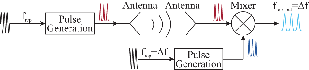
In the frequency domain, this offset leads to the generation of classical sum- and difference-frequencies between the spectral components, yet only the differences of adjacent, detuned tones fall into the low-frequency range of interest. In the time domain, the process corresponds to subsampling, where individual frequency components of the transmitted signal are sampled by the receiver pulses. The amplitude and phase information of the original high-frequency signal is thus mapped onto the much lower alias frequency  $f_\mathrm{alias}=f_\mathrm{sig}-N\cdot f_\mathrm{s}$, i.e., the relative deviation from an integer multiple of the sampling rate. Consequently, the composite transmit signal, consisting of multiple frequency components, is effectively converted into a low-frequency comb, which appears broadened in the time domain and can be easily sampled and analyzed, while retaining the information. As illustrated in Figure 2, the transceiver architecture comprises a transmitter and a receiver, each including a pulse generator and an antenna. The receiver further incorporates a mixer for the dual-comb down-conversion. This work presents the design of the transmitter section, with particular emphasis on different concepts for signal generation. An earlier version of this paper was presented at EuMW 2025 and was published in its Proceedings [Reference Krylova, Aufinger and Pohl6].
Block diagram of the proposed pulse-based dual-comb transceiver for distance and thickness measurements. The dual-comb principle describes mixing of two time-domain pulse trains with slightly different repetition rates, producing broadened pulses that enable sampling and analysis.

Pulse generation circuits
PIN-diode-based pulse generator
In this work, two circuit concepts for THz pulse generation are investigated. Both designs are introduced together with their implementation, and their main features are compared at the end to highlight advantages and limitations.
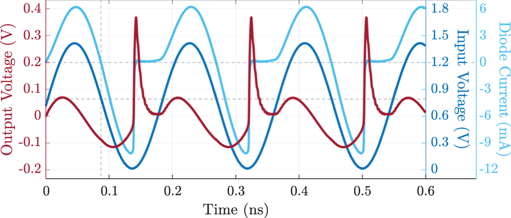
The operation of the PIN diode pulse generator relies on the reverse-recovery effect, which distinguishes it from a conventional PN diode by the presence of an intrinsic layer. Under forward bias, once the applied voltage exceeds the threshold, the diode enters forward conduction; charge carriers are injected into the intrinsic region, where excess charge is stored. When the bias is reduced, the diode experiences reverse conduction, as these carriers must first be removed before it can block. During this depletion process, the current continues to flow and follows the waveform of the excitation voltage. Once the stored carriers are fully extracted, the diode is unable to sustain conduction, and the current abruptly drops to zero [Reference Tien and Hu7]. The sharp current edge inherently contains multiple frequency components. The slope of such a rise corresponds to a pulse: the steeper the edge, the narrower and higher the waveform. To obtain these values, the current is differentiated by an inductive load, e.g., an EM-simulated planar coil, resulting in a voltage pulse, as illustrated in Figure 3.
PIN diode reverse recovery simulation at  $f_\mathrm{rep} =$ 5.5 GHz. The inductive load differentiates the resulting sharp current edge into an 8 ps voltage pulse.

From the simulation, one drawback of this concept becomes evident: the limited isolation between input and output causes the sine component at the repetition rate to be superimposed on the generated pulses. As long as its amplitude remains significantly lower than that of the pulses, however, this has no further impact on system functionality.
The PIN-diode-based circuit was implemented in Infineon’s 90 nm B12HFC technology, which offers bipolar performance of  $f_\mathrm{T}/f_\mathrm{max} $= 300/530 GHz [Reference Böck, Aufinger, Knapp, Mukherjee, BWohlmuth, Komenko, Rothenhauber, Tschumakow and Stavrev8]. Within this process, PIN diodes are not created as dedicated design elements but are rather available as a byproduct of the process layer stack originally intended for the bipolar devices. Consequently, their reverse recovery and switching properties have only been described by physical approximations rather than specific models. To characterize their behavior, 12 test structures were fabricated, incorporating diodes based on 2 available device options in the layout (pdiode and varactor), of 3 different sizes, both with and without inductive load. The realized layouts are shown in Figure 4. Since the reverse-recovery slope is determined by the amount of stored charge in the intrinsic region, smaller stripe lengths (i.e., the segmented anode fingers contacting the intrinsic region) inherently lead to faster depletion and thus steeper current edges. Therefore, the minimum available stripe length of 5
 $\unicode{x03BC}$m was selected. To further investigate the scaling behavior, two even smaller 2.5 and 1
 $\unicode{x03BC}$m versions were created by manually cropping the diode layout, aiming for steeper slopes, narrower pulses, and thus higher bandwidth for the intended application.
Micrograph of the fabricated PIN-diode test circuits, featuring different stripe lengths and layout variations used for the reverse-recovery evaluation.

Push-pull pulse generator
The second investigated pulse-generation approach is an active transistor-based circuit, designed to improve port isolation and enable operation at lower input power levels. As with the PIN diode, voltage pulses are obtained by differentiating the current edges, which in this case appear in a push-pull amplifier driven by differential square-wave control signals, as shown in Figure 5(a). The abrupt switching of a high current between the differential paths produces steep rising and falling transitions, leading to both positive and undesired negative pulses at the output. To suppress the latter, the current source can be periodically disabled via a pMOS transistor switch.
Push-pull pulse generator: (a) circuit schematic adapted from [Reference Hasenaecker, Rein, Aufinger, Pohl and Musch9], where the rising edge of the switching current through the inductive load generates voltage pulses at the output; (b) chip micrograph of the fabricated circuit with a functional core size of 434 $\times$393
 $\unicode{x03BC}$m
 $^2$ (excluding bias pads).

Figure 5 Long description
Panel a draws a symmetrical circuit. Four transistors labelled T1 to T4 sit inside a dashed box marked transistor core, T1 and T2 above T3 and T4, with a capacitor labelled C1 bridging the middle of the pair. Their common lower node runs to a current source labelled I above a ground symbol. Two inputs enter at the left, one marked with a square wave symbol labelled U. Above the core, two inductors labelled L meet at a centre tap. Each side reaches an output terminal through a capacitor labelled C out, with a resistor labelled R to ground beyond it. Small symbols mark a rising pulse on the left branch and a falling pulse on the right. Panel b photographs the chip, a tall rectangle with square bond pads down both long edges. Leader lines name an inductive load and a transistor core near the top, a preamplifier below, a functional core inside a dashed outline, and two DC bias structures lower down. Two pads at the foot read IN plus and IN minus. Edge arrows give 1360 by 740 micrometres.
This transistor-based circuit is realized in IHP’s 130 nm SG13G3 technology with  $f_\mathrm{T} $= 470 GHz and
 $f_\mathrm{max} $= 610 GHz [Reference Rücker, Heinemann and Bärwolf10]. A micrograph of the fabricated pulse generator Monolithic Microwave Integrated Circuit (MMIC) is shown in Figure 5(b). To shape the sinusoidal input into a differential square-wave control signal, a preamplifier stage precedes the main circuit. It employs the same push-pull topology as the core, but with a resistive load and smaller transistors operated in saturation as switches, thereby clipping the input signal amplitude and generating the required waveform. In the main schematic, each differential branch of the amplifier contains an inductive load for signal derivation, which is combined in the layout to a center-tapped inductor. A cascode stage is employed above the input devices to suppress the Miller effect and thus maintain sharp current transitions. To sustain the high current, 3 of the available 8-fold npn devices are connected in parallel for each of the transistors in the original schematic, corresponding to 24 transistors in total. Nevertheless, the largest area consumption results from the coupling capacitors. At the output,
 $C_\mathrm{out}$ provides DC isolation to protect the measurement equipment, requiring large capacitance values to avoid filtering out lower harmonics. Similarly, capacitors between the transistor core and the preamplifier ensure independent biasing and optimized operating points for both circuits. In particular,
 $C_1$ enables separate biasing of the cascode transistors to compensate for the slight asymmetry between rising and falling edges of the current. By tuning the bias at the transistor base, the transition times can be adjusted, resulting in more uniform pulse shapes.
Measurement results
Measurement setup
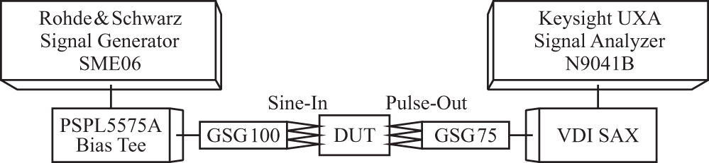
To characterize the behavior of the pulse-generating circuits, the measurement equipment must capture the full spectral bandwidth of the pulses. For picosecond durations, this extends well beyond 100 GHz, exceeding the bandwidth of available oscilloscopes and rendering direct time-domain evaluation impractical. Therefore, the circuits were analyzed in the frequency domain, with separate measurements carried out for all relevant bands. The measurement setup diagrams were previously reported in [Reference Krylova, Aufinger and Pohl6].
In both configurations, a Rohde  $\&$ Schwarz signal generator provided the input signals, defining the output pulse repetition rate, while bias voltages were delivered using a separate power supply through a bias tee or DC-probe. The circuits were contacted on-chip using suitable 100
 $\unicode{x03BC}$m-pitch probes, and the output spectra were captured with a Keysight UXA analyzer at 50
 $\Omega$ input impedance. For the transistor-based circuit, the differential architecture required excitation through a 180
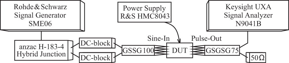
 $^{\circ}$ hybrid junction converting the single-ended source, which is depicted in Figure 6. The output was contacted with a GSGSG probe, with one branch terminated off-chip at 50
 $\Omega$ and the other connected to the UXA. The absence of this probe configuration at higher frequencies limited the measured range for this generator to 110 GHz. To expand the characterization beyond 110 GHz and cover harmonics above the 20th order, waveguide extenders for WR 10, WR 6.5, WR 5.1, WR 3.4, and WR 2.2 bands were employed together with the corresponding probes, as illustrated in Figure 7. While WR 10 itself does not extend beyond 110 GHz, it was used to obtain accurate results below this limit without driving the UXA to its maximum range. Their frequency-dependent attenuation was taken into account when merging the spectra and evaluating all 12 individual PIN-diode-based circuits. Figures 8 and 10–12 are adapted from an earlier version of this paper [Reference Krylova, Aufinger and Pohl6].
Measurement setup for spectrum analysis of the transistor-based pulse generator. The configuration represents a differential setup, with excitation provided via a 180 $^{\circ}$ hybrid junction and balanced probing of the output.

Measurement setup for spectrum analysis of the PIN-diode-based pulse generator. The output is analyzed from DC to WR 2.2 frequency band using waveguide extenders, enabling characterization of harmonics up to 500 GHz.

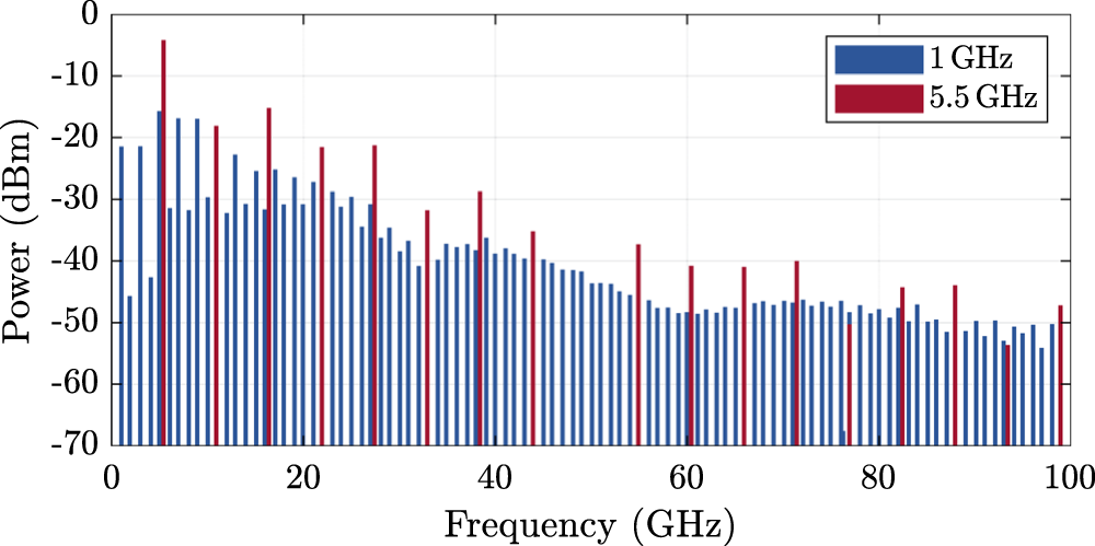
Measured spectra of the transistor-based pulse generator at 5.5 and 1 GHz input. At 1 GHz, the harmonic levels are uniformly reduced, as the available power is spread across more components. The captured span is limited by the probe bandwidth.

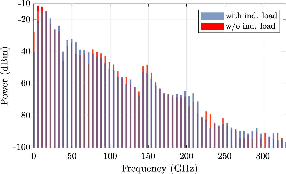
Measured spectrum of the PIN-diode-based pulse generator (5  $\unicode{x03BC}$m pdiode), obtained by merging data from different bands. The combined spectra confirm the harmonics of the 5.5 GHz repetition rate across the entire frequency range.

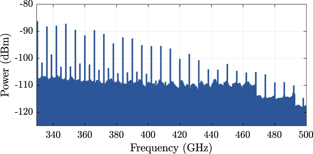
Measured spectrum of the PIN-diode-based pulse generator at 6 GHz input frequency using a WR 2.2 SAX. The observed harmonics indicate broadband pulse behavior across the measurement range and remain above the noise floor, with bandwidth settings reflected in the step-like baseline.

Transient pulse train: (a) transistor-based, simulated. Voltage pulse attains 6.4 V peak at 10.4 ps pulsewidth; (b) PIN-based, simulated and reconstructed from merged spectra under a zero-phase assumption for all harmonics. The latter provides a 273 mV peak at 13.2 ps, cf. 7.6 ps at 1 V simulated. Both pulse trains exhibit a repetition rate of 5.5 GHz consistent with simulation.

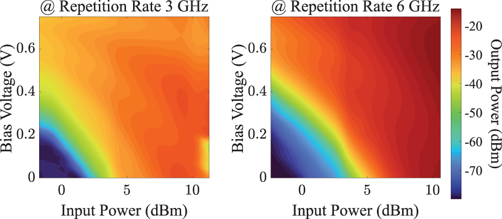
Measured power of a selected output harmonic in a PIN-diode pulse generator as a function of input power and bias voltage. Bias shifts the operating point and enables harmonic generation at reduced input levels, while the required voltage to maintain a harmonic level decreases with rising excitation.

Results
The transistor-based pulse generator was characterized directly with a signal analyzer at different input frequencies. The observed spectra resemble the expected behavior of the two-stage push-pull architecture. The first amplifier operates in saturation, generating a square-wave output with pronounced odd harmonics, which then serves as the control signal for the second stage to perform abrupt current switching. Most importantly, the inductive load differentiates the current into a voltage pulse, simultaneously suppressing low-frequency components and emphasizing higher-order harmonics due to its inherent frequency-dependent behavior. As a result, while a steady decline is present in the output current spectrum, the fundamental and third harmonic power at 1 GHz repetition rate appear lower than that of the higher-order components, even though the overall envelope still decreases toward higher frequencies.
For lower pulse repetition rates, the available power is distributed across a larger number of harmonics within the fixed frequency span, thereby reducing the power per harmonic. Consequently, the measurement requires longer acquisition times, as the resolution bandwidth must be minimized to separate the signal from the noise floor. Figure 8 illustrates the output spectra at 5.5 and 1 GHz input. Both curves follow the same trend, with their value difference only slightly deviating from the expected 10 $\cdot$
 $\log$(5.5) = 7.4 dB. As the measurement range was limited to 110 GHz, many relevant spectral components could not be captured, which prevented experimental pulse reconstruction. Thus, the pulse shape of the transistor-based generator was derived solely from simulation (Figure 11(a)).
Based on these observations, the PIN-diode-based circuits were characterized at 5.5 GHz, close to the upper limit of the available signal generator. Frequency-domain measurements extended up to 500 GHz, and the merged spectra confirmed the expected harmonics of the repetition rate, characteristic of a pulse spectrum, across the entire range shown in Figure 9. The spectra with and without an inductive load coincided with the simulations, with the main deviations occurring at DC and the fundamental, where inductive derivation led to significantly reduced values. Across 12 test circuits, both layout components (pdiode and varactor) exhibited consistent results, confirming that the two modeling approaches are equally suitable for the design. For the upper measurement frequency limit in the WR-2.2-band, the components are depicted in Figure 10 at 6 GHz input. Although the output power decreases at higher frequencies, the harmonics remain distinctly above the thermal noise floor. The necessary adjustments of resolution and video bandwidths are reflected in the step-like variations in the noise floor baseline.
Pulse reconstruction was performed by inverse Fourier transformation under the assumption of zero phase difference, since the incoherent spectra of the PIN diode cannot provide phase information. While the pulse shape is determined by the spectral phase and the reconstruction result is therefore not unique under incoherent measurement conditions, assuming zero phase does not reflect the true waveform but provides a deterministic estimate of the achievable peak amplitude and pulsewidth. Assigning a common phase across all harmonics corresponds to the limiting case suggested by the Fourier series expansion of a Dirac comb. The finite measurement bandwidth alone, however, already leads the reconstruction toward a weighted Dirichlet-kernel-like response, producing broader and lower-amplitude pulses. This effect is further amplified by the attenuation of higher-frequency components owing to the low-pass characteristics inherent to the measurement setup. The reconstructed train, shown in Figure 11(b), demonstrates a distinct pulse every 181.8 ps, corresponding to a repetition rate of 5.5 GHz in the time domain. The pulsewidth (FWHM) was determined as 13.2 ps at a peak voltage of 273 mV, while the simulation for the same input power resulted in values of 7.6 ps and 1 V, respectively. Under phase deviation, instead of constructive interference forming a narrow pulse, the spectral components tend to appear temporally misaligned, further altering the pulse shape. Even wideband oscilloscope measurements cannot directly capture the undistorted waveform due to setup-induced degradation, such as limited cutoff frequencies, dispersion and frequency-dependent losses in cables, probes, and interconnects. As demonstrated in [Reference Khoeini, Hadidian, Zhang and Afshari11], reflection-based short pulses were de-embedded, reducing the apparent pulsewidth from 13 ps at 210 mV to 6.8 ps at 680 mV. A coherent measurement is required to compare the generated pulsewidths of the derived pulses in six test circuits, since the expected differences lie in the sub-picosecond range. Simulations indicate pulsewidths of 9.9, 9.2, and 8 ps for stripe lengths of 10, 7.5, and 5  $\unicode{x03BC}$m, respectively. While the lack of phase information complicates the experimental estimation of the true pulse shape and its characteristic parameters, this limitation affects only the measurement setup and not the actual performance of the pulse generator. The achievable pulsewidth and resolution in the final transceiver are determined solely by the system architecture and can fully contribute to the radar measurement. In the final industrial dual-comb sensor, the radiated and subsequently received amplitude and phase information can be preserved and shifted to lower frequencies, where they are coherently processed to ensure the required measurement accuracy. A 7.6 ps pulsewidth translates into a range resolution of 1.1 mm for the desired application. These results exceed what is possible with existing FMCW radar systems and highlight the potential of the proposed generator concept.
Increasing the input power enhances the amplitude of the output harmonics, which is generally beneficial for the pulse generator. However, higher input levels also raise the voltage drop across the PIN diode and are therefore limited to avoid diode damage and excessive signal power dissipation. A bias voltage can compensate for reduced input power by shifting the diode’s operating point. Figure 12 illustrates this effect by showing the measured amplitude of a selected harmonic as a function of input power and bias voltage. At low signal levels, the diode remains beneath its switching threshold and does not operate effectively, resulting in negligible output. With bias applied, the operating point is adjusted, enabling the diode to generate significant harmonic output even at reduced excitation. As the input level rises, the required voltage to maintain the harmonic level decreases, as reflected in the diagonal transition of the contour plot from low to high amplitude. Beyond a certain input level, additional bias voltage becomes disadvantageous, as the diode no longer exhibits proper reverse recovery. This demonstrates that biasing is particularly beneficial in the low-power regime, whereas at higher input levels the generator performance is determined by the available input power itself.
When comparing the two implemented pulse generator concepts, the PIN-diode-based design achieves a simulated pulsewidth reduction of 27 $ \%$, which translates into increased spectral bandwidth and improved range resolution compared to the transistor-based circuit. The architecture remains simple, as all harmonics are generated by a single PIN diode, with the planar coil being the only component that requires notable area. Consequently, the core footprint can be reduced by more than 55
 $ \%$, simultaneously lowering parasitic effects. In addition, the PIN-diode circuit operates passively apart from the bias supply, whereas the transistor-based generator requires 272 mW of DC power. The advantages in area and power efficiency make the PIN-diode approach particularly well suited for the intended application. The transistor-based concept offers the benefit of differential architecture, provides input-output isolation, and delivers a substantially higher output peak voltage at low input power. This enables an extended system range, which remains a key advantage of the active design.
To provide a comparison with state-of-the-art systems, Table 1 summarizes the pulsewidth, resulting range resolution, output amplitude, and a brief description of the generator architecture. The compared sources report only measured or simulated pulsewidths and were not evaluated in an actual distance-measurement scenario. Therefore, the possible range resolution is derived solely from the FWHM. While [Reference Khoeini, Hadidian, Zhang and Afshari11] mentions the unity-gain frequency of a preamplifier and [Reference Razavian and Babakhani4] provides a 10 dB Equivalent Isotropic Radiated Power (EIRP bandwidth, the output pulses were captured in the time domain, and the spectral evaluation is strongly affected by the measurement setup. Since the system bandwidth of a pulse generator is largely determined by the pulse shape [Reference Sala, Kenney-Wallace and Hall12], i.e., by an assumed model that differs from the real measured pulse, a comparison based on this parameter is not reliable and is therefore not included as a separate metric.
State-of-the-art comparison of pulse generating systems

Table 1 Long description
The table compares six pulse generation systems: two from this work, characterized in the frequency domain and four in the time domain from prior references, listing pulsewidth, range resolution and peak voltage. Each entry mentions technique and technology. -This Work, PIN-diode with inductive load, 90 nm SiGe: Pulsewidth 7.6 ps, resolution 1.1 mm, peak voltage 1.0 V. Data origin: simulated. -This Work, push-pull current steering, 130 nm SiGe: 10.4 ps, 1.6 mm, 6.4 V; data simulated -Ref. 4, edge-sharpening and PIN diode, 90 nm SiGe: 1.7 ps, 0.25 mm, 0.006 V (measured) and 0.63 V (simulated); measured with an optical sampling system; data extracted from plot Following measured with a wide-band oscilloscope: -Ref. 11, amplifier and reflection-based, 110 nm CMOS: 6.8 ps, 1.0 mm, 0.68V and 8.8 ps, 1.3 mm, 1.0V; de-embedded -Ref. 13, SRD-based generator and two NLTLs, R04350 PCB: 10.8 ps, 1.6 mm, 3.5 V -Ref. 14, square-wave split-signal, 250 nm InP HBT: 8.4 ps, 1.3 mm, 0.435 V; de-embedded
a Simulated. b Measured. c Extracted from plot. d De-embedded.
Compared to state-of-the-art systems addressing the picosecond regime, both presented architectures achieve FWHM and amplitude values consistent with other pulse generators characterized in the time domain, while providing a combination of these parameters that is particularly relevant for thickness measurement applications and maintaining a comparatively simple architecture. Although [Reference Razavian and Babakhani4] reports a sub-2-ps pulse, this result corresponds to a complete transmitter measured using a THz optical sampling system and therefore does not reflect the constraints of on-chip characterization or of a standalone pulse generator.
Pulse-based transmitter
Design and implementation
Despite the measures taken to de-embed the influence of the measurement setup, it can still significantly affect the observed power spectra. The probing pad itself exhibits a parasitic capacitance of approximately 25 fF, which forms a low-pass filter with a cutoff frequency of approx. 127 GHz, as per  $f_\mathrm{c}=1/(2\pi RC)$. The realization of a pulse-based transmitter incorporating the designed pulse generator represents a significant step toward a complete transceiver system, while providing a means to overcome the measurement limitations inherent to standalone generator characterization.
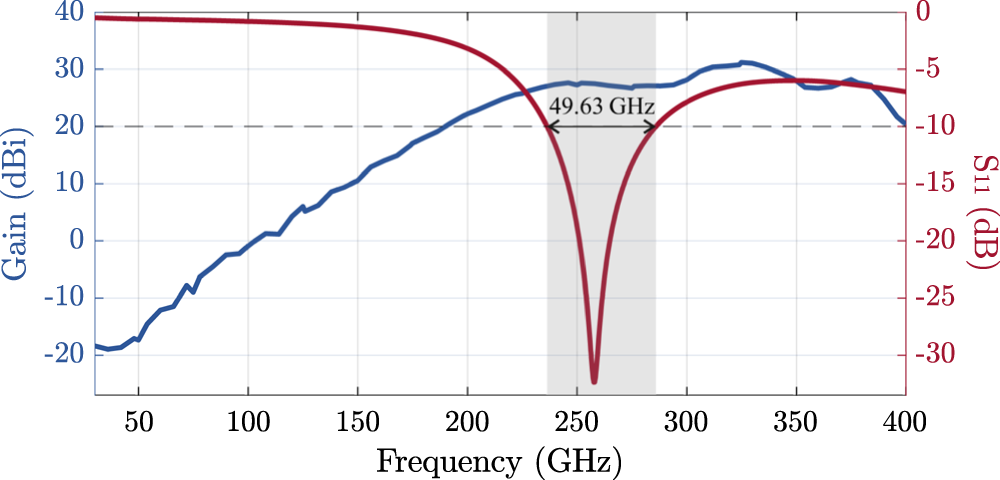
The transmitter was fabricated in Infineon’s B11HFC 130 nm BiCMOS technology, with the transistors reaching  $f_\mathrm{T}/f_\mathrm{max}$ of 250 and 370 GHz, respectively [Reference Böck, Aufinger, Boguth, Dahl, Knapp, Liebl, Manger, Meister, Pribil, Wursthorn, Lachner, Heinemann, Rücker, Fox, Barth, Fischer, Marschmeyer, Schmidt, Trusch and Wipf15]. The realized MMIC is presented in Figure 13. The PIN diode approach was utilized, as its verified spectral components extend into the frequency range where compact on-chip antennas can be realized, ensuring consistency between generator and transmitter characterization. The circuit consists of two pulse generators, as introduced in Figure 4, jointly driving a differential folded-dipole antenna with a self-resonant frequency of 258 GHz and a
 $-$10 dB return loss bandwidth of 19
 $ \%$ (Figure 14). The folded dipole was selected as it provides higher impedance and moderately enhanced bandwidth compared to a conventional dipole [Reference Vallecchi, De Luis, Capolino and De Flaviis16], while offering a straightforward solution for verifying the circuit functionality. Each generator integrates a single PIN diode with an inductive load. In one generator, the diode is oriented in reverse and negatively biased to enable negative pulse generation, thereby establishing a semi-differential circuit operation. Additional design adjustments were made to accommodate technology-specific differences in the metal layer stack.
Chip micrograph of the realized transmitter circuit (854 $\times$420
 $\unicode{x03BC}$m
 $^2$). The architecture comprises two PIN diodes oriented in opposite directions, each with an inductive load, corresponding to two pulse generators that feed a folded-dipole antenna.

Simulated main lobe direction gain of the antenna-lens combination, reaching 27.5 dBi at the antenna resonance frequency of 258 GHz, as confirmed by the S $_{11}$ response.

Measurement setup
To characterize the designed transmitter, a dedicated assembly was required. A printed circuit board (PCB) was designed to provide connectors for input and bias signals to the chip. The PCB thickness was chosen to be 250  $\unicode{x03BC}$m, enabling thinner microstrip lines with 50
 $\Omega$ single-ended and 100
 $\Omega$ differential impedance, while also facilitating bond-wire interconnects to the MMIC. Instead of relying on elaborate cavity fabrication, the PCB incorporates a through-hole for the MMIC in the center, as the height difference to the chip is only around 60
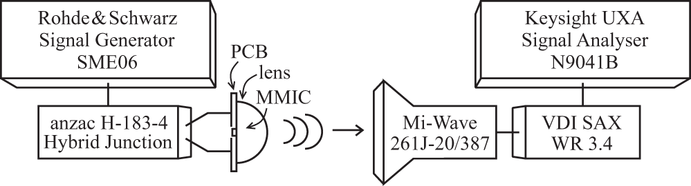
 $\unicode{x03BC}$m. For assembly, the setup consisting of the MMIC, PCB, and a BATOP LSA-D20-T13.77 collimating silicon lens was realized in two steps: first, the lens was glued to the PCB using a UV-reactive adhesive; and second, the MMIC was inserted through the PCB opening and placed onto the lens prior to the final adhesive curing in a thermal chamber. The silicon lens was chosen to minimize interface reflections along the radiation path. Moreover, downward emission through the chip suppresses substrate modes, as no ground plane is present beneath the antenna region. The proposed antenna-lens combination demonstrates a simulated peak gain of 27.5 dBi at 258 GHz, as shown in Figure 14. The frequency-dependent gain variation across the band can be attributed to the resonance characteristics of the folded-dipole antenna. The completed assembly was mounted on a 3D-printed custom fixture attached to a PI DT-80 compact rotation stage driven by a PI C-663 stepper motor controller. The single-ended input signal is once again generated by a Rohde & Schwarz signal generator and converted into a differential waveform by an Anzac hybrid junction, defining a pulse repetition rate of 6 GHz. The radiated signal propagates through the MMIC, the PCB opening, and the collimating lens toward the target. It is received by a Mi-Wave 20 dBi J-band horn antenna and forwarded to a Keysight UXA signal analyzer via a VDI WR 3.4 SAX, thereby covering the entire transmitter antenna bandwidth. The polarization of the horn antenna was aligned with that of the on-chip folded dipole to ensure efficient coupling. A block diagram of the described measurement setup is shown in Figure 15.
Measurement setup for spectrum analysis of the pulse-based transmitter. DC-bias is provided off-chip to enable both positive and negative pulse generation. The on-chip antenna radiates through the chip and silicon lens.

Measurement results
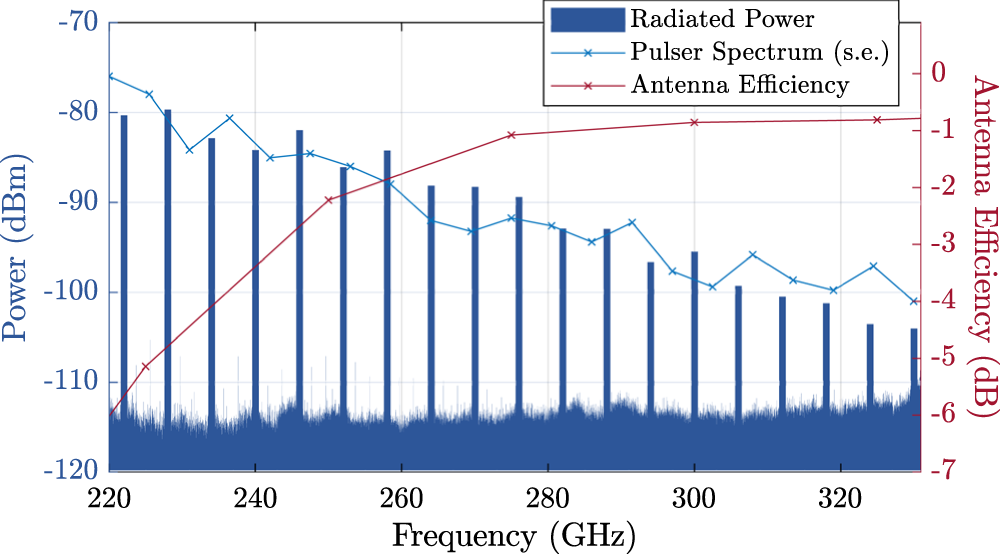
To maintain a sufficient signal-to-noise ratio, the measurement was conducted in the radiating near-field, so the received power is determined by the antenna efficiency, including material losses, and by the geometrical setup properties, rather than by free-space path loss and antenna gain, thereby representing the captured radiated power instead of a far-field EIRP. In this regime, only a fraction of the signal radiated through the 20-mm lens is coupled into the WR-3.4 antenna with an aperture of 2.9 $ \times $4 mm, already reducing the received power by 14.4 dB under the assumption of a uniform field distribution. The horn aperture efficiency of approximately 70% and alignment tolerances between transmitting the antenna, the lens, and the receiver, as well as the frequency-dependent coupling between them, further contribute to the reduced signal levels. The measured radiated power of the designed transmitter, after deembedding the influence of the measurement setup, including cable, extender, and the coupling losses described above, is shown in Figure 16. In direct comparison, the measured spectrum of the single-ended pulse generator, as shown in Ch. 2, and the simulated antenna efficiency of the folded-dipole antenna are presented. The radiated power exhibits a decline across the measured frequency range. At the lower end of the band, this decrease is mitigated, as the increasing antenna efficiency compensates for the reduced harmonic levels. Beyond the antenna resonance frequency of 258 GHz, the efficiency approaches its saturation value, and the radiated power follows the pulse generator spectrum. With that, the expected harmonic behavior at the anticipated frequencies, and thus the functionality of the transmitter, has been verified.
Measured de-embedded transmitter radiated power, with the frequency-dependent decrease determined by the countereffect of rising antenna efficiency and declining harmonic power.

As the mounting height and the rotation of the board around the vertical axis were manually adjusted to direct the emitted beam towards the target, the influence of possible misalignment was investigated by varying the turning angle between  $-$30
 $^{\circ}$ and 30
 $^{\circ}$ in 3
 $^{\circ}$ steps using the rotation stage. Figure 17 shows the angular dependence of the transmitter radiated power for all measured harmonics in the J-band, corresponding to an azimuthal cut of the transmitter radiation pattern. The main-lobe waveform follows a consistent trend, while value fluctuations appear primarily outside the main lobe and beyond the antenna bandwidth. These variations become visible at low signal levels and can be attributed to multipath reflections in the tabletop laboratory setup, despite the use of absorber material around the receiving horn, as well as small vertical and axial tolerances introduced by mechanical misalignment of the transmitter mounting. At the antenna resonance frequency of 258 GHz, the 3 dB beamwidth is slightly off-center, spanning 0
 $^{\circ}$ to 12
 $^{\circ}$, which underlines the need for accurate board alignment due to angular sensitivity.
Measured transmitter radiated power as a function of angular rotation, illustrating misalignment sensitivity with a 3 dB beamwidth of 12 $^{\circ}$ at 258 GHz.

Conclusion
This work demonstrated the development of a pulse-based transmitter as a solution for broadband transceiver systems, aiming to overcome existing range resolution limits. As a key component of such architecture, two pulse generation approaches were realized and characterized. The PIN-diode-based circuit demonstrated compact and energy-efficient operation, achieving a simulated 6 dB pulsewidth of 7.6 ps at 1 V amplitude and a 5.5 GHz repetition rate, with spectral components experimentally verified up to 500 GHz, enabling measured pulse reconstruction. In addition, the transistor-based fully differential concept delivered high output voltage, providing a 6.4 V output pulse with a comparable pulsewidth of 10.4 ps and a spectrum characterized up to 110 GHz, thereby offering increased range.
Building upon these results, the extension from a standalone pulse generator to a complete pulse-based transmitter was realized. Two PIN-diode-based pulse generators were combined in semi-differential operation and connected to a folded-dipole antenna, forming the transmitter design. The circuit was integrated into an assembly with a custom PCB and a collimating silicon lens, which enabled downward radiation through the MMIC, thus suppressing substrate modes. The measured radiated power confirmed the expected spectral behavior in the J-band around the antenna resonance at 258 GHz. Although the antenna does not radiate the entire pulse bandwidth, the measured spectral section provides proof of concept for the pulse-based transmitter and validates system functionality, as all harmonics within this band were consistently generated and radiated. The successful implementation of the proposed pulse generator has thus been demonstrated, proving the suitability of this approach for pulse-based transceiver systems.
Future work will focus on completing the transceiver architecture by integrating an ultra-wideband mixer to enable pulse reception and allow full system measurements. In addition, an alternative antenna concept will be investigated to specifically address the lower cutoff frequency and increase the fraction of the generated spectrum that is effectively radiated. With these improvements, a complete system-level evaluation for high-resolution thickness measurements can be performed. Ultimately, the presented architecture offers a promising foundation for future inline sensing scenarios that require high resolution, while providing the advantages of a compact, robust, and fully integrated design.
Funding statement
This work was supported by the “European Regional Development Fund” and the “Just Transition Fund” (EFRE/JTF 2021-2027) from the Ministry of Health, Equalities, Care and Ageing of the State of North Rhine-Westphalia as part of the project TIGER (Grant EFRE-20800194).
Competing interests
The author(s) declare none.

Olga Krylova received her B.Sc. and M.Sc. degrees in electrical engineering and information technology from the Ruhr-University Bochum in Bochum, Germany, in 2021 and 2024, respectively. She is currently pursuing her Ph.D. degree with a major in electronics within the TopING program at the same university. Her research focuses on mm-wave integrated circuits for measurement applications, e.g., broadband transceiver systems at terahertz frequencies. Her studies were recognized by the IEEE MTT-S Undergraduate Scholarship 2024 and the VDE Rhein-Ruhr Graduate Award 2025.

Andrii Berdnykov received the B.Sc. and M.Sc. degrees in electrical engineering and information technology from Ruhr-University Bochum, Germany, in 2021 and 2024, where he is currently working towards the Ph.D. degree. Since 2024, he has been a Research Assistant with the Institute of Integrated Systems, Ruhr University Bochum. His current research interests include the design and analytic synthesis of sub-terahertz and ultra-wideband integrated circuits and on-chip antennas in SiGe BiCMOS technologies.

Klaus Aufinger (Senior Member, IEEE) received the Diploma and Ph.D. degree in physics from the University of Innsbruck, Innsbruck, Austria, in 1990 and 2001, respectively. From 1990 to 1991, he was a Teaching Assistant with the Institute of Theoretical Physics, University of Innsbruck. In 1991, he joined the Corporate Research and Development of Siemens AG, Munich, Germany, where he investigated noise in submicrometer bipolar transistors. He is currently with Infineon Technologies AG, Neubiberg, Germany, the former semiconductor Group of Siemens, Munich, working in the field of device physics, technology development, and modeling of advanced SiGe technologies for high-speed digital and analog circuits. He also gives lectures on analog bipolar technology at the Technical University of Munich, Munich, Germany. He has coauthored more than 200 publications in scientific journals and conferences. Dr. Aufinger was a member of the Technical Program Committee of the IEEE International Electron Devices Meeting (IEDM). He is also a reviewer for several journals and European Microwave Week (EUMW).

Nils Pohl (Fellow, IEEE) received the Dipl.-Ing. and Dr.Ing. degrees in electrical engineering from Ruhr University Bochum, Bochum, Germany, in 2005 and 2010, respectively. From 2006 to 2011, he was a Research Assistant at Ruhr University Bochum, Bochum, Germany, where he was subsequently an Assistant Professor in 2011. In 2013, he became the Head of the Department of mm-Wave radar and high-frequency sensors with the Fraunhofer FHR, Wachtberg, Germany. Since 2016, he has been a Full Professor of integrated systems at Ruhr University Bochum, while also maintaining a part-time affiliation with Fraunhofer FHR. He is currently a Supervisor of 27 Ph.D. students and several PostDocs. He is also involved in several third-party-funded research projects and is a co-founder of the start-up 2Pi-Labs. He has authored or coauthored more than 300 scientific papers and has issued several patents. His research interests include ultra-wideband mm-wave radar, design and optimization of mm-Wave integrated SiGe circuits and system concepts with frequencies up to 500 GHz, frequency synthesis, and antennas. He is actively involved in the scientific community, having worked on the Program Committees of IMS, EUMW, RWW, SIRF, BCICTS, GEMIC, IMWS-AMP, and EUCAP. He is a reviewer for several IEEE journals, has been a Guest Editor for IEEE Transactions on Microwave Theory and Techniques, and is also an Associate Editor for Transactions on Radar Systems. He was the Chair of the MTT TC 24 Microwave/mm-Wave Radar, Sensing, and Array Systems Committee and the spokesman of the microwave section in the German VDE/ITG. He was the recipient the Karl-Arnold Award from the North Rhine-Westphalian Academy of Sciences, Humanities and the Arts in 2013, the International IHP “Wolfgang Mehr” Fellowship Award for research in high-frequency electronics in 2017, IEEE MTT Outstanding Young Engineer Award in 2018, and the VDE-ITG Award in 2023. He was also the co-recipient of the Best Demo Award at RWW 2015, Best Student Paper Awards at RadarConf 2020, RWW 2021, and EuMIC 2021, and Best Paper Awards at EuMIC 2012, AWPL 2022, and SENSL 2023. He is also a member of VDE, ITG, EUMA, and URSI.

Tobias T. Braun (Member, IEEE) was born in Duesseldorf, Germany, in 1996. He received the B.Sc. and M.Sc. degrees in electrical engineering and information technology from TU Dortmund, Dortmund, Germany, in 2016 and 2019, respectively, and the Ph.D. degree in electrical engineering and information technology from Ruhr University Bochum, Bochum, Germany, in 2024. From 2019 to 2025, he was a Research Assistant with the Institute of Integrated Systems, Ruhr University Bochum, where he has since become the Institute’s Chief Engineer. His research interests include integrated circuit and system design for automotive applications, low-noise synthesizers for space observation, and nonlinear radar systems. Dr. Braun was the recipient of the EuMIC Young Engineer Prize from European Microwave Week in 2021, Honorable mention winner of the 3MT competition at the International Microwave Symposium 2022, and second place winner of the Student Paper Competition at Radio & Wireless Week 2025.










 Open access

