The adsorption and reactivity of oxygen on nickel surfaces has attracted considerable research effort over the last 40 years. An atomic-scale understanding of this complex interaction offers fundamental insights crucial to many important technological processes such as corrosion, bulk oxidation in electronic systems, and heterogeneous catalysis. The chemisorption of oxygen on the (100) surface of nickel at room temperature has been well documented.[Reference Kopatzki and Behm1–Reference Holloway and Hudson3] Molecular oxygen dissociates at the surface and an oxygen monolayer of p(2 × 2) or c(2 × 2) arrangement forms prior to the nucleation of epitaxial nickel monoxide (NiO) nuclei. The adsorption of oxygen and subsequent nucleation of the oxide phase can be highly dependent on the presence of topographical defects such as surface vacancies.[Reference de esús, Pereira, Carrazza and Zaera4] Moreover, scanning tunneling microscopy (STM) studies have demonstrated that monatomic steps on a vicinal surface provide the most active sites for NiO nucleation on Ni(100)[Reference Baumer, Cappus, Kuhlenbeck, Freund, Wilhelmi, Brodde and Neddermeyer5] and Ni(111).[Reference Hildebrandt, Hagendorf, Doege, Jeckstiess, Kulia and Neddermeyer6] Dislocations also play a major role in surface reactions; for example, the catalytic activity of nickel has long been known to increase upon cold rolling.[Reference Eckell7] Superficial steps associated with near-surface dislocations are likely to influence the oxygen adsorption and oxidation activity in several ways, including altered local electronic structure, lower atomic coordination, and facilitated migration of charged adsorbate species. In this study, using controlled in situ indentation in the STM we induce deformation structures with well-defined topographies, interpreted as dislocation loops intersecting the surface. We record the tunneling current–voltage characteristics with high spatial resolution, using the same STM tip in scanning tunneling spectroscopy (STS) mode as a measure of local electronic density of states (LDOS). On average, the LDOS around the Fermi level (E F) taken at surface steps where dislocations terminate is enhanced and shifted higher in energy as compared with the LDOS distribution at flat, undeformed terraces. Furthermore, we report accelerated oxidation kinetics at dislocation steps, which we attribute to the modification of electronic structure by atomic undercoordination at these sites.
A (100)-oriented Ni specimen (99.999% purity, Ames Laboratory, Ames, IA, USA) was first mechanically polished on the (100) face finishing with a 1 µm diamond slurry. The crystal was then electrochemically polished using a Struers LectroPol-5 electrolytic polisher/etcher in 40% H2SO4 solution at 12 V for 40 s. The polished surface area was roughly 60 mm2. The sample was placed in an ultra-high vacuum (UHV) analysis chamber at <109 mbar and cleaned by repeated cycles of high-temperature degassing (1100 K, 1–5 min), Ar+ sputtering (500 meV, 5 min), and annealing (1000 K, 2–3 h). STM was performed under UHV at room temperature using an O micron AFM/STM system (VT STM, Omicron Nanotechnology, GmbH, Taunusstein, Germany). A custom-made dual indentation/tunneling tip was made by attaching a B-doped diamond coated atomic force microscopy (AFM) cantilever tip (DDESP, Bruker SPM Probes, Camarillo, CA) to a q-Plus non-contact AFM sensor using conductive epoxy glue.[Reference King, Lamb and Nunes8] Line scans revealed the nickel surface to be cut at roughly 2° to the (100) direction, comprising terraces of 50 nm width separated by monatomic steps. The root-mean-square surface roughness at terraces was around 0.5 Å. In situ indentations were performed during STM using the “z-ramp” function of the STM controller (MATRIX, Omicron Nanotechnology, GmbH, Taunusstein, Germany). The tip was stepped toward the sample surface by a specified amount during scanning. Indentations of varying depths between 0.5 and 20 nm could be formed. One example is shown in Fig. 1. The surface electronic structure of the dislocation regions and flat terraces were probed in situ by STS. Finally, ultra-high-purity oxygen (>99.99%) was introduced via a leak valve in the direct vicinity of the Ni(100) single crystal at a pressure of 10−6 mbar for various durations corresponding to total oxygen doses of 10 and 100 Langmuirs, L. Following each dose the surface was immediately imaged at high resolution (scan sizes of 100 × 100 nm2) under vacuum at <10−9 mbar.
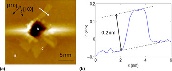
In situ topographical characterization of induced plastic deformation formed by indentation with the STM tip. (a) Indentation of single-crystal Ni(100): A denotes the indented region, B the undeformed, atomically flat terrace, and C a surface step formed by the coherent nucleation and propagation of dislocations; (b) line trace taken along the arrow shown in (a) indicates a step height of 0.15–0.2 nm. Imaging conditions: sample bias of −0.3 V, feedback tunneling current 1 nA.

The step-like features observed around indentations characteristically progressed along 〈110〉 directions with cross-slip segments along 〈100〉 (Fig. 1), similar to those observed by Carrasco et al.[Reference Carrasco, Rodriguez de la Fuente, Gonzalez and Rojo9] on Au(100) using STM indentation. A likely mechanism for their formation is as follows: indentation with the STM probe leads to the nucleation of shallow dislocation loops (<20 nm from the surface) consisting of a segment parallel to the surface and two emergent sections of predominantly screw character. Where the screw dislocation lines intersect the surface, a step of height  is created and is dragged along as the dislocation further glides on a {111} plane. For nickel, such a step would have a height given by (a/2)(110)(100) = 0.176 nm, where a is the lattice parameter. This is consistent with our measurements of 0.15–0.2 nm [Fig. 1(b)]. Multiple cross-slip of screw dislocations on adjacent, sub-surface {111} planes can generate steps appearing to point along 〈001〉 directions on the surface, probably comprising many small orthogonal 〈110〉 oriented steps.[Reference Navarro, Rodriguez de la Fuente, Mascaraque and Rojo10]
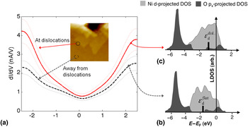
STS was conducted immediately following indentation. The tunneling current I was measured as a function of sample bias voltage V from −2.5 to +2.5 eV. This encompasses a reasonable spread of electron energies in the vicinity of the Fermi level E F, over which the Ni d-states and O p-states hybridize in the oxidation of the surface.[Reference Castell, Wincott, Condon, Muggelberg, Thornton, Dudarev, Sutton and Briggs11] Tunneling spectra were obtained both at wide, undeformed, atomically flat terraces [e.g., region B in Fig. 1(a)] and directly at step edges associated with dislocation loops [Fig. 1(b)]. Between 20 and 50 discrete point spectra were acquired for each feature of interest, from each of the nine independent experiments taken with different STM tips, under the same imaging conditions and within 30 min of indentation with the STM probe. During tunneling spectra acquisition, there was no identifiable drift on the imaged surface; throughout this time the chamber base pressure remained in the low 10−10 mbar range. Further, there was no significant accumulation of surface contamination, as would be indicated by new image features or roughening of the topography that could affect the electronic structure measurements. Averaged over all measurements obtained during each experimental trial, the distribution of electronic states around E F at surface-terminated dislocations could be directly compared with states from nearby, dislocation-free surface regions [Fig. 2(a)]. Differential tunneling conductance dI/dV was obtained by numerical differentiation of a polynomial smoothing spline approximation to give a comparative measure of the LDOS.[Reference Ukraintsev12] A statistically significant enhancement in I and dI/dV around E F was observed at dislocations compared to flat terraces. In most cases the enhancement in LDOS was greatest under negative bias between −1 and −2.5 eV.
(a) In situ electronic structure characterization of the Ni(100) surface upon STM tip-induced plasticity. Differential tunneling conductance measurements, dI/dV, obtained both at dislocation steps (solid curve) and away from dislocations (dashed curve). Each curve is the average of over 100 point spectra from three different indentations. The error in dI/dV measured by standard deviation is ±18%, represented by dashed enveloping curves. Schematic density of state diagrams illustrate how an increase in DOS around E F can be interpreted as an up-shift in the Ni d-band center from (b) ɛ dflat at the undamaged surface to (c) ɛ ddisl at dislocations (after [14]).

We interpret these results in the framework of the d-band model proposed by Hammer and Norskov.[Reference Hammer and Norskov13] To a first approximation the center of mass of the d-band electrons, ɛ d, of the unreacted surface is the underlying parameter determining surface reactivity for transition metals, including nickel. Oxygen is a molecular adsorbate with partially empty states above the Fermi level of nickel. Small changes in the local environment can lead to substantial shifts in d-band energy and hence in the hybridization energy of adsorbed oxygen species, whose bonding and antibonding states shift in energy congruently with ɛ d [Fig. 2(b) and (c)]. A shift in ɛ d toward higher energies pushes the oxygen antibonding states up relative to E F, further emptying those electronic levels, strengthening adsorption, and therefore reducing the barrier to molecular dissociation. This general trend has been widely observed, with d-band shifts arising from alloying,[Reference Holmblad, Larsen, Chorkendorff, Pleth Nielsen, Besenbacher, Stensgaard, Loegsgaard, Kratzer, Hammer and Nørskov14] epitaxial strain,[Reference Mavrikakis, Hammer and Nørskov15] and surface topology.[Reference Ruban, Hammer, Stoltze, Skriver and Nørskov16] To our knowledge, this is the first application of such a model to plastic deformation-induced shifts in LDOS and the corresponding surface reactivity towards oxidation.
Steps such as those observed in Fig. 1(a) are formed through strain relaxation where dislocations intersect the surface. The local coordination number of atoms is reduced at the dislocation step edges with respect to the flat surface. This causes a shift in the Ni d-band center toward higher energies concurrent with the narrowing of Ni d-states in energy, while maintaining the same d-band filling. In this study we observed an increase in LDOS most evidently within 1.5–2.5 eV below E F at dislocation steps as compared with undamaged terrace regions; this can be interpreted alternatively as an overall up-shift in energy of ɛ d. Consequently, we expect these dislocated regions to exhibit preferential adsorption properties toward molecular species such as oxygen, as explained above. Moreover, since the metal d-states are closer to the Fermi level, we expect facilitated electron transfer to oxygen and consequently a tendency for greater activity at surface-terminated dislocations during the incipient stages of oxidation.[Reference Feibelman and Hamann17, Reference Yang and Parr18]
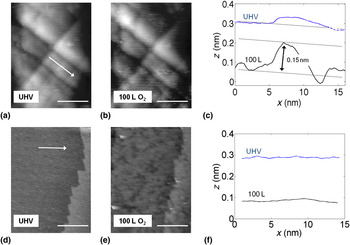
To confirm this we conducted in situ oxidation experiments in STM by repeatedly exposing the Ni(100) surface to oxygen followed each time by imaging in UHV. Oxygen doses of 10–100 L at room temperature have been used to probe the formation kinetics of oxide nuclei, in the form of small protrusions of 0.15–0.2 nm height in the z-axis, on Ni(100)[Reference Kopatzki and Behm1, Reference Baumer, Cappus, Kuhlenbeck, Freund, Wilhelmi, Brodde and Neddermeyer5] and Ni(111).[Reference Hildebrandt, Hagendorf, Doege, Jeckstiess, Kulia and Neddermeyer6] In the present experiments, small protrusions of precisely this height appeared to form preferentially on and along dislocation steps [Fig. 3(a) prior to oxidation and Fig. 3(b) after oxidation]. This correlation in height between our present measurements and previous measurements of nickel oxide nuclei dimensions strongly suggests that these new surface features appearing at dislocation steps in the oxygen environment were nickel oxide nuclei and islands. A greater spatial density of bright spots (oxide islands) was found at the linear step-like dislocation features as compared with flatter regions [Fig. 3(d)] after 100 L O2 exposure. We note that over the course of obtaining images at base pressure (on the order of 10−10 mbar) both prior to and following O2 exposure—a process that took between 30 min and 1 h to image several adjacent locations and correct for scan drift—no observable increase in the number of oxide islands per unit area occurred. We conclude that there was no systematic contamination of the surface by other species during imaging at base pressure that could be misinterpreted as oxidation of nickel. These findings contribute toward a unified picture of plasticity-enhanced reactivity of transition metal surfaces to oxygen, and by extension to other small reactive molecules.
STM images of dislocation steps (perpendicular linear features) created by STM tip indentation: (a) immediately following indentation under UHV and (b) after exposure to 100 L O2. (c) Line traces along the white arrow direction corresponding to images (a) and (b). (d) STM image of the atomically flat surface and pre-existing terrace step under UHV with the corresponding image (e) taken after 100 L exposure for comparison. (f) Line traces corresponding to the arrow direction in (d) and (e). Imaging conditions: −0.15 V, 1 nA. Scale bar: 20 nm.

In summary, we have demonstrated the capability to form well-defined nanostructures on the Ni(100) surface associated with dislocation loops via in situ STM indentation and interrogate these using STS to measure their influence on surface reactivity. We consistently measured an increase in I and dI/dV within 2.5 eV on either side of E F, most prominently below −1.0 eV. The increase in LDOS at dislocations compared with perfect terrace surfaces of the crystal is interpreted as an up-shift in the nickel d-band states toward higher energies. This affects the interaction with reactive molecular species by lowering the energy barrier to dissociative chemisorption and by facilitating electron transfer. Hence dislocation steps, from an electronic structure perspective, are likely to provide preferential nucleation sites for chemical reactions. Direct evidence for this was provided through in situ observations of the early stages of oxidation in this work. A greater density of NiO nanoislands was found to form around dislocation-stepped areas than on flat, undamaged surfaces. This novel experimental approach offers a means to obtain unique insights into the coupling of mechanical damage to chemical reactivity at the atomic level, which contributes to diverse fields such as stress-driven corrosion and catalysis.
Acknowledgments
BY thanks the Nuclear Regulatory Commission Young Faculty Grant Programme, and BY and KJVV thank the BP's Inherently Reliable Facilities Programme for financial support on this research.
Supplementary materials
For supplementary material for this article, please visit http://dx.doi.org/10.1557/mrc.2011.17