I. INTRODUCTION
Smart sensors are effective means to collect useful information for us from ambient environment, which is getting more and more important especially with the fast development of internet of things (IoT). Smart sensors have already penetrated into every corner of our daily life, such as industrial production, marine exploration, environmental protection, resource investigation, medical diagnosis, biological engineering, even the protection of cultural relics, and so on. It is no exaggeration to say that various sensors are indispensable to the complicated engineering systems for many modern projects, which is critical to the human economic development and social advancement. Reference Wang, Lin, Chen, Niu and Zi1–Reference Zhang, Chen, Lin, Deng, Zhang, Zhang, Zhu, Yang and Wang9
Over the past decades, various kinds of sensors for health monitoring, environmental protection, infrastructure detecting, and security have been developed. Reference Zhou, Zhu, Niu, Liu, Bai, Jing and Wang10–Reference Fan, Lin, Zhu, Wu, Zhang and Wang14 It is said that the world will have trillions of sensor cells positioned on the world by 2020. Reference Wang, Chen and Lin15 The recent development of IoT and sensor networks rapidly changes the traditional understanding about power need. Powering these sensor nodes relies on rechargeable batteries, which may not be the favorable solution for IoT. Since the increasing amount of batteries owing to the rapid explosion of mobile electronics may result in challenges for batteries recycling and replacement as well as the concerns of potential environmental pollution. Reference Yeh, Lin, Yang and Wang16–Reference Bai, Zhu, Liu, Chen, Jing, Yang, Zhang, Ma and Wang23 Mechanical motion ubiquitously exists in ambient environment and people’s daily life. In recent years, it becomes an attractive target for energy harvesting as a potentially alternative power source to battery operated electronics. Reference Hou, Yang, Zhang, Chen, Chen and Wang24–Reference Yang, Chen, Jing, Yang, Wen, Su, Zhu, Bai and Wang34
As one of the most ubiquitous natural phenomena, triboelectrification is often regarded as a negative effect that in most cases was avoided by many technologies. Recently, Zhong Lin Wang’s group in Georgia Institute of Technology has invented a fundamentally new energy technology, triboelectric nanogenerator (TENG), relying on the coupling of contact electrification and electrostatic induction. As an inventive energy collector, TENG harvests energy through contact electrification of two opposite tribo-polarity materials, which can convert the mechanical motions of two triboelectric layers into electrical potential difference between electrodes, and drive the electrons to flow back and forth in the external circuit. Reference Park, Kim, Vosgueritchian, Cheon, Kim, Koo, Kim, Lee, Schwartz, Chang and Bao35–Reference Yang, Zhang, Liu, Lin, Lee, Lin, Wong and Wang44 The materials used for the fabrication of TENG are common and widely available, such as paper, fabrics, polydimethylsiloxane (PDMS), polytetrafluoroethylene (PTFE), aluminum (Al), polyvinylchloride (PVC), and fluorinated ethylene propylene (FEP) Reference Zhu, Bai, Chen and Wang45–Reference Li, Chen, Zhou, Zheng, Fan, Wen, Yu and Wang52 . And it was demonstrated to collect energy from a wide range of mechanical motions, for example, human motion, Reference Yi, Lin, Niu, Yang, Wang, Chen, Zhou, Zi, Wang, Liao, Zhang and Wang53 vibration, Reference Zhang, Yang, Su, Chen, Adams, Lee, Hu and Wang54 rotation, Reference Jing, Zhu, Bai, Xie, Chen, Han and Wang55 wind blowing, Reference Quan, Han, Jiang and Wang56 sound wave, Reference Yu, Pan, Chen, Zhu and Wang57 water flow, Reference Lin, Cheng, Wu, Pradel and Wang58 rain drop, Reference Zhang, Yang, Su, Chen, Hu, Wu, Liu, Wong, Bando and Wang59 ocean wave, Reference Jiang, Zhang, Chen, Han, Tang, Zhang, Xu and Wang60 and so on. Reference Fang, Tong, Zhong, Chen, Chou, Luo, Zhou, Wang and Hu61–Reference Zhang, Zhang, Chen, Jin, Deng, Tang, Zhang, Pan, Zhu, Yang and Wang63 The working modes of TENG are rather diverse and could be applied to harvest most of conventional mechanical/kinetic motions in our daily life. Not only they can convert mechanical motions into electrical signals, TENGs can also be used as self-powered sensors to detect displacement, velocity, metallic ion, humidity, temperature, and ultraviolet (UV) intensity. Reference Niu, Wang, Lin, Liu, Zhou, Hu and Wang64–Reference Niu, Liu, Wang, Lin, Hu and Wang66 In this paper, we presented a comprehensive review of the self-powered smart sensors based on TENG with a start of introducing the TENG working principles, then the device structural design, materials usage, and the smart sensors for practical applications, with an end of summarization of the perspectives and challenges for the TENG based self-powered smart sensors.
A. Working principles of the TENG
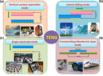
The working principle of TENGs relies on a coupling effect of the contact electrification and the electrostatic induction. As known, contact electrification is a widely existed phenomenon that one material becomes charged after it contacts another material with opposite electron affinity. Reference Zi, Wang, Wang, Li, Wen, Guo and Wang67,Reference Zhang, Zhang, Yang, Zhou, Han and Wang68 Though it is one of the most experienced effects in daily life, the mechanism behind triboelectrification is still under exploration. Reference Wu, Wang, Lin, Guo and Wang69–Reference Niu, Liu, Chen, Wang, Lin, Hu and Wang71 It is generally believed that during the physical contact of two materials, some of the bonded atoms have a tendency to keep extra electrons and some a tendency to give them away, producing triboelectric charges at the interface. Reference Zhong, Zhang, Zhong, Hu, Hu, Wang and Zhou72–Reference Su, Zhao, Li, Yuan, Wang, Cao and Zhu74 The triboelectric charges on dielectric surfaces can be a driving force to make electrons flow back and forth among electrodes. Reference Li, Chen, Guo, Fan, Wen, Yeh, Yu, Cao and Wang75–Reference Li, Zhang, Duan, Zhang, Wang, Dong and Wang77 And four different working modes of TENGs have been established and presented, Reference Wang78 as illustrated in Fig. 1.
Four fundamental working modes of triboelectric nanogenerators: (a) vertical contact-separation mode; (b) lateral sliding mode; (c) single-electrode mode; and (d) freestanding triboelectric-layer mode. Reproduced with permission from the Royal Society of Chemistry. Reference Wang78

1. Vertical contact-separation mode
As illustrated in Fig. 1(a), two dissimilar dielectric films with back-coated electrodes are facing each other. Reference Yang, Chen, Zhu, Yang, Bai, Su, Jing, Cao and Wang79 The physical contact between a pair of dielectric films will generate opposite triboelectric charges on their surfaces. Once a physical gap induced between the two surfaces by the external mechanical motion, a potential difference was created. The periodic contact and separation between the two charged surfaces will induce a periodic electric potential difference between the paired electrodes, which will drive the electrons to flow back and forth in the external circuit.
2. Lateral sliding mode
The structure of this mode is the same as that of the vertical contact-separation mode. When two dielectric films are brought into contact with each other, a relative in-plane sliding against each other also generates charges on the contact surfaces [Fig. 1(b)]. Therefore, transversal polarization occurs in the sliding direction, which drives the electrons on the back electrodes to flow to fully balance the electrical potential difference created by the triboelectric charges. Reference Zheng, Cheng, Chen, Lin, Wang, Liu and Wang80 A periodic sliding back and forth generates an alternating current output. This is the in-plane sliding mode TENG. The sliding motion can be extended to a cylindrical rotation or a disc rotation. Reference Lin, Xie, Wang, Wu, Niu, Wen and Wang81
3. Single-electrode mode
The previous two working modes need paired electrodes connected to external load, which will greatly confine the movement of the triboelectric layers. In some cases, one of the triboelectric layers needs to be a mobile object, such as human walking on the floor. Reference Yang, Zhang, Lin, Liu, Chen, Lin, Zhou, Wong and Wang82 A single-electrode mode TENG was thus developed to solve this problem in which the only electrode in the TENG is grounded [Fig. 1(c)]. When the top object approaches or leaves the triboelectric layer, it will also change the distribution of the local electric field, which would lead to a flow of electrons moving back and forth between the electrodes and ground. In this working mode, relative motion of the triboelectric layer can also be classified as vertical contact-separation and in-plane sliding motions.
4. Freestanding triboelectric-layer mode
The nonmobile triboelectric charges could sustain a long period of time on the contact surface. Reference Zhu, Chen, Liu, Bai, Zhou, Jing, Pan and Wang83 When there is a symmetrical electrode under the dielectric layer, the objects close to and away from the electrodes will cause the electrons to flow between the two electrodes to balance the local potential distribution [Fig. 1(d)]. The conversion of mechanical motions into electricity does not need the direct physical contact between the two triboelectric layers, which effectively prevents the materials abrasion during TENG operation. This is a decent design to improve the durability of TENGs.
II. TENG AS A TACTILE SENSOR
The sensors for instantaneous detection of interfacial pressure are of critical importance to the applications of touch screen, security monitoring, healthcare, and so on. Reference Zhu, Lin, Jing, Bai, Pan, Yang, Zhou and Wang84–Reference Zhu, Zhou, Bai, Meng, Jing, Chen and Wang86 Owing to the unique advantage of the single-electrode TENG that one of the triboelectric layer can move freely, which makes it especially suitable for the detection of touch from a foreign object.
Zhu et al. Reference Zhu, Yang, Zhang, Jing, Chen, Zhou, Bai and Wang87 proposed a self-powered triboelectric sensor (TES) based on vertically laminated thin-film materials [Fig. 2(a)]. To start with, the structure of TES is supported by a polyethylene terephthalate (PET) layer consisting of two layers of indium tin oxide (ITO) on its back and front sides. On the front side, FEP layer can produce triboelectric charges through contact with other objects. The surface of FEP is modified by vertically aligned polymer nanowires (PNWs). The average length of PNWs can reach 1.5 μm and a diameter of 150 nm. The PNWs layer is a significant part in achieving high sensitivity for low-pressure detection. A nylon film with excellent mechanical and thermal performance plays as a protection layer on the back side.
A self-powered, flexible, and ultrasensitive tactile sensor: (a) schematic structure of the tactile sensor; (b) a scanning electron microscope (SEM) image of the polymer nanowires created on the surface of the FEP thin film; (c) photograph of the tactile sensor for sensing a foreign object; (d) measurement of open-circuit voltage with a cyclic contact force of 20 mN; (e) summarized results of the output voltage under different contact pressures. Inset: an enlarged view of the summarized results at low-pressure region; (f) a photograph showing that the TES was integrated with a signal processing circuit to turn on the siren alarm when a human hand touched the door handle; (g) a photograph showing that the TES was integrated with another signal processing circuit to turn on light when it was contacted by a human finger. Reproduced with permission from the American Chemical Society. Reference Zhu, Yang, Zhang, Jing, Chen, Zhou, Bai and Wang87

Formed with general thin-film materials, the TES is cost-effective. With such structural design and fabrication process, the TES is also suitable for large-scale fabrication. To evaluate the sensing performance of the device, a square-shaped TES in Fig. 2(c) was manufactured to discover metal through cyclic contact and separation. As shown in Fig. 2(d), the maximum output voltage of the TES can reach 35 V when the applied pressure is about 0.03 kPa. With the increasing of contact pressure up to 10 kPa, the output voltage reaches 50 V [Fig. 2(e)]. With PNW modification, the TES obtains a high pressure sensitivity of 44 mV/Pa (0.09% Pa−1), and a maximum sensitivity of 1.1 V/Pa (2.3% Pa−1) in a low-pressure region (<0.15 kPa). With flexible structure, the TES can be fabricated with any size and shape, even onto curved surfaces. Additionally, a full wireless sensing system can also be developed through integration of the TES with a signal processing circuit. The output voltage generated by the TES to trigger an IC (integrated circuit) timer plays an important role in the whole system, which controls a wireless transmitter. When a human hand touched the door handle, the remote system will immediately start to operate [Fig. 2(f)]. The system has been utilized successfully in various applications, such as human-electronics interface, detection, remote operation, and security systems. In the process of replacing other functional devices for the wireless transmitter in the circuit, the sensing system has been successfully applied in a wide range of applications, such as a touch-enabled switch for a panel light shown in Fig. 2(g).
III. TENG AS A VIBRATION SENSOR
As one of the widely existed mechanical motions in our daily life, vibration holds a variety of forms and can be found from mechanical equipment, transportation, construction, and even ocean tide. Reference Chen, Zhu, Yang, Jing, Bai, Yang, Hou and Wang88 Since the working condition of machineries and infrastructures can be evaluated by their vibrations, numerous transducers have been developed for monitoring and detecting ambient mechanical vibrations. Owing to the conversion from vibrational motions into electrical signals, TENG becomes an excellent self-powered sensor for ambient vibration detection.
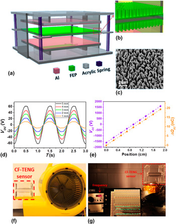
The vibration frequency is usually easy to be quantified by vibration sensors, but it is hard to measure the vibration amplitudes. Here, Wang et al. proposed a method to quantitatively measure the vibration amplitude by fabricating a contact-mode freestanding triboelectric nanogenerator (CF-TENG). Reference Wang, Niu, Yang, Lin and Wang89 The structural design of the device is schematically shown in Fig. 3(a). The acrylic was shaped by a laser cutter to form the framework of the TENG. Two front-to-front structured Al-coated acrylic slices which served as electrodes of the CF-TENG are separated with a gap distance of 2 cm. In between, another acrylic sheet served as the vibration resonator connected by 4 pairs of springs at the four corners to the top and bottom acrylic substrates. To enhance the triboelectric charge density, the FEP surface is etched by the inductive coupling plasma (ICP) reactive ion etching, which produced nanowire structures [Fig. 3(b)] to increase the surface roughness and the effective surface area. The diameter of nanowires is about 100 nm, and the length is about 1 μm [Fig. 3(c)]. As shown in Fig. 3(d), the linear motor followed sinusoidal motions. Because of the linearity for electricity generation, the profiles of V oc are sinusoidal waves, but with a π/2 phase shift. When the resonator vibration amplitudes were gradually increased up to 5 mm with a fixed vibration frequency of 1 Hz, the increasing of V oc is propositional to the vibration amplitude, which can be expected from their relationships with the resonator moving distance. A good linearity in the electricity generation behavior makes the CF-TENG to quantitatively measure the vibrational amplitude with utmost capability. To experimentally demonstrate it, the electrical signals of the CF-TENG were measured under a series of different vibration amplitudes at constant vibration frequency. As shown in Fig. 3(e), with the expanding of vibrational amplitude, the peak-to-peak value of V oc increases directly, as well as the amplitude of I sc when the shaker’s amplitude is within the range below 1.5 mm. Figure 3(f) shows that the CF-TENG did well in monitoring the vibration from a wind blower’s operation. From the demonstration of Fig. 3(g), the generated electricity could power up to 60 LEDs with a vibration amplitude of 1.5 cm and frequency of 15 Hz.
Contact-mode freestanding triboelectric nanogenerator: (a) schematic diagram showing the typical device structure of a CF-TENG; (b) enlarged view of the device structure showing the nanowire structure on the surface of the FEP films attached on the resonator plate; (c) SEM image of the nanowire structures on the FEP films; (d) five groups of V oc profiles when the motor was set with sinusoidal motions at the same frequency (1 Hz) but five different amplitudes; (e) simulated open-circuit voltages and short-circuit charge densities of the CF-TENG at different positions of the resonator plate; (f) photograph showing the demonstration of using the CF-TENG to monitor the vibration of a wind blower during its operation; (g) 60 LEDs instantaneously driven by the CF-TENG. Reproduced with permission from the American Chemical Society. Reference Wang, Niu, Yang, Lin and Wang89

Moreover, Hu et al. Reference Hu, Yang, Jing, Niu, Wu and Wang90 introduced a TENG based on the spiral structure (STENGs) as vibration and positioning sensor. As shown in Fig. 4(a), the STENG works in a vertical contact and separation mode. With light weight, proper strength, easy processing, acrylic is available for the structural material. The two face-to-face round slices work to create electricity in Fig. 4(a) lined with red. One round plate connects the 3D spiral structure and the other attached on the cube’s bottom. The diameter of nanopores arranged on the aluminum surface in Fig. 4(b) is about 30 nm for enhancing the effective contact area of TENG. Figure 4(c) shows the nano-modified Kapton surface, which can enhance the output performance due to the increasing of surface roughness and the effective contact area of the STENG. There are 3 STENGs fixed on a test board with a size of 1 × 24 × 48 in. for the vibration source position [Fig. 4(d)]. On the test board, nine positions were chosen to be monitored by 3 STENGs, as the experimental setup illustrated in Fig. 4(e). The load weighed 100 g is used to hit the test board, with the different height of L (L = 1, 2, 3, 4, and 5 cm) and acceleration (a = 1, 2, 3, 4, 5, 6, 8, and 9.8 m/s2). As shown in Fig. 4(f), the dependence of the load falling acceleration on the STENGs voltage output was studied with a height L of 5 cm. And the voltage output is an increasing function of the acceleration, since the larger the landing acceleration, the higher the momentum onto the board. And the relevance of the monitored voltage/current signals and mass landing momentum was measured and demonstrated in Fig. 4(g). Figure 4(h) presented the measured results with different vertical falling heights and accelerations, which all follow a linear relationship between the output signal and the landing mass momentum.
Triboelectric nanogenerator built on suspended 3D spiral structure as a vibration and positioning sensor: 3D TENG spiral structure (a) and schematic diagram of the device and its cross section view; SEM image of the surface morphology of (b) aluminum and (c) the Kapton film; (d) schematic diagram of the experimental setup shows three STENGs positioned at the three corners of a wooden board as a self-powered dynamic sensor; (e) schematic diagram of the experimental setup; (f) recorded voltage signals when the mass is released from L = 5 cm at different accelerations; (g) measured voltage/current signals with different mass load momentum at L = 5 cm; (h) comparison of measured voltage signals under different testing conditions. A linear relationship is revealed. Reproduced with permission from the American Chemical Society. Reference Hu, Yang, Jing, Niu, Wu and Wang90

IV. TENG AS AN ACOUSTIC SENSOR
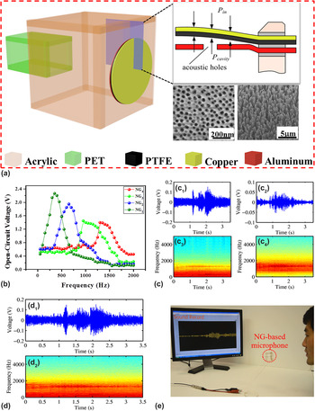
Sound waves widely exist in the environment around us. And it has been lack of effective technology to convert it into electricity since the sound wave itself holds very low power density. Yang et al. Reference Yang, Chen, Liu, Yang, Su and Wang91 developed an organic thin-film based TENG to harvest environmental acoustic wave as a sustainable power resource and self-powered acoustic sensor. As indicated in Fig. 5(a), relying on a Helmholtz cavity with a size-tunable narrow neck, the circular shape with a multilayer structure plays a critical role in acoustic energy harvesting. In the device, one electrode is the Al film with nanoporous surface and the other is copper, which was back-coated on the PTFE film. As shown in Fig. 5(b), four TENGs as an array were integrated together to extend the whole device operation bandwidth from 10 to 1700 Hz, which made it possible for self-powered human voice recording. Figures 5(c1) and 5(c3) show time domain waveforms of the recorded sound by nanogenerator NG1 and NG4. As demonstrated in Figs. 5(c2) and 5(c4), the waveform of NG4 was rough since its natural frequency is 1400 Hz, while NG1 one was smooth owing to its natural frequency of 350 Hz, which is the dominant frequency response for the range from 10 to 600 Hz. To reconstruct the original sound, the acquired acoustic signals of the array are weighted according to the relative amount of information obtained from each source. The waveform of the rebuild signal and its corresponding short-time Fourier transform are shown in Figs. 5(d1) and 5(d2). Figure 5(e) indicates an as-manufactured TENG serving as a self-powered microphone to record sound.
Triboelectric nanogenerator for self-powered active acoustic sensing: (a) sketch and structural design of the triboelectric nanogenerators; (b and c) demonstration of the TENG acting as a self-powered microphone; frequency responses from the nanogenerator array, which consists of four NGs with various designed natural frequencies, aimed to enhance the overall working bandwidth; (c1 and c2) sound waveforms of the signals acquired by NG1 and NG2, respectively; (c3, c4) short-time Fourier transforms of the acquired signals by NG1 and NG2, respectively; (d) sound waveform and corresponding short-time Fourier transform of the signals acquired by the array of NGs; (e) photograph that shows an NG working as a self-powered microphone for sound recording. Reproduced with permission from the American Chemical Society. Reference Yang, Chen, Liu, Yang, Su and Wang91

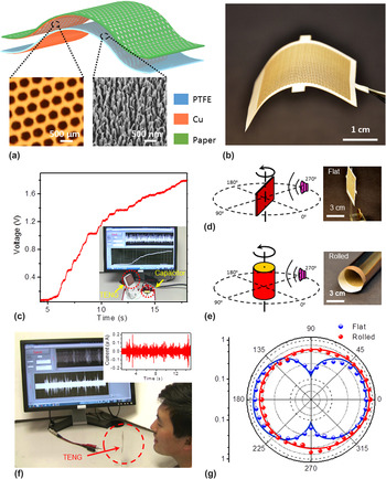
Moreover, Fan et al. Reference Fan, Chen, Yang, Bai, Li and Wang92 reported an ultrathin, rollable, paper-based TENG to harvest acoustic energy and record sound in a self-powered manner. As illustrated in Fig. 6(a), the supporting substrate of TENG is a layer of multiholed paper, which is coated with copper as electrode. From Fig. 6(b), we can know that the TENG is as thin as 125 μm. With outstanding characteristics of thinness, flexibility, widen-bandwidth, and independence of resonator, the presented TENG is unique in acoustic energy harvesting. As shown in Fig. 6(c), the capacitor was charged to 1.8 V just in 12 s by the power recycled from the sound of a cell phone. Figures 6(d) and 6(e), respectively, illustrate the principle of measuring the directional patterns of the flat and rolled TENG. As demonstrated in Fig. 6(f), the paper-thin TENG was capable of recording sound and acting as a self-powered microphone. Different structures of the TENG corresponded to different directional patterns [Fig. 6(g)]. The flat one had a butterfly shaped directional pattern with mirror symmetry, while the rolled one has round-shape directional pattern, which is feasible for theatric stage live recording, military surveillance, and omnibearing acoustic energy harvesting.
Paper-based TENG for acoustic energy harvesting and self-powered sound recording: (a) schematic illustrations of the paper-based TENG; (b) photograph of the multihole paper electrode; (c) recycling the acoustic energy from the cell phone via charging a 2 μF capacitor; schematic illustrations to show the measurement of the directional patterns of the (d) flat and (e) rolled paper-thin triboelectric nanogenerator and right sides are the photographs of the as-fabricated device; (f) photograph that shows a paper-thin triboelectric nanogenerator as a self-powered microphone for sound recording. Inset is the acquired electrical signals; (g) shape dependent directional patterns of the paper-based TENG with flat and rolled structure, respectively. Reproduced with permission from the American Chemical Society. Reference Fan, Chen, Yang, Bai, Li and Wang92

V. TENG AS A BIOMEDICAL SENSOR
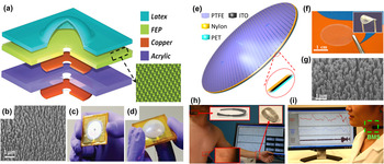
Smart sensors play an important role in our life by catching characteristics of human physiology or behavior. Self-powered sensor based on TENG could also be used for biomedical monitoring purpose. Here, Bai et al. Reference Bai, Zhu, Jing, Yang, Chen, Su, Ma, Zhang and Wang93 developed a membrane-based triboelectric sensor (M-TES) for air pressure detection and health monitoring. As shown in Fig. 7(a), M-TES is consisted of an acrylic sheet of 1.6 mm as the substrate, a copper layer of 100 nm as the electrode, FEP layer of 125 µm, and latex layer of 50 µm. The photograph in Fig. 7(b) indicates that the average size of nanorod on FEP layer is 130 nm of diameter and 500 nm of length. The device is packaged with epoxy resin in the edges of layers. Figure 7(c) presents an image of the M-TES with an area of 3.2 cm2. As demonstrated in Fig. 7(d), the latex layer becomes expanded and then separated away from the FEP layer, when the inside pressure was changed owing to the human motions via the air-conducting channel. With small size and lightweight, M-TES could be used everywhere for air pressure detection. The sensor presents a resolution of 0.34 Pa with air pressure increasing and 0.16 Pa with air pressure decreasing. With further miniaturization, the sensor will reach higher sensitivity, which makes it suitable for self-powered human biomedical monitoring.
Self-powered biomedical sensor based on a TENG: (a) illustration of the membrane-based self-powered sensors for pressure change detection; (b) SEM image of the polymer nanowires on the FEP surface; (c and d) photograph of the as-fabricated real device. Reproduced with permission from Wiley. Reference Bai, Zhu, Jing, Yang, Chen, Su, Ma, Zhang and Wang93 (e) Schematic illustration of the self-powered bionic membrane sensor; (f) photograph of the as-fabricated bionic membrane sensor; (g) SEM image of the PTFE nanowires; (h) photograph showing that the as-fabricated bionic membrane sensors were directly attached to simultaneously monitor the pulse waves of the participant from his carotid artery, chest, and wrist; (i) photograph showing that the bionic membrane sensor was worn against the participant’s neck acting as a self-powered throat microphone. Reproduced with permission from Wiley. Reference Yang, Chen, Su, Jing, Li, Yi, Wen, Wang and Wang94

Furthermore, Yang et al. Reference Yang, Chen, Su, Jing, Li, Yi, Wen, Wang and Wang94 reported a self-powered bionic membrane sensor (BMS), which is flexible, lightweight, low-cost, simply fabricated, and capable of operating in a multimodal way for biomedical monitoring and biometric authentication. As illustrated in Fig. 7(e), the BMS holds a multilayered structure with PET layer at the bottom as substrate and the ITO layer as electrode. Then, a layer of nylon was laminated on the ITO, followed by a tented PTFE layer on the top to form a conical cavity. A pair of holes with diameters of 0.5 mm was punched through the BMS bottom layers, serving as channels to communicate with the environmental air [Fig. 7(f)]. To promote the triboelectrification, nanowires were arranged on the surface of the PTFE layer [Fig. 7(g)]. To operate, the vibration mode of the PTFE layer in the BMS changed in diverse frequencies. Multiple BMSs were utilized to detect human pulse in different artery positions, which can capture more data for human cardiovascular risk estimation. Figures 7(h) and 7(i) demonstrated the capability of BMS, respectively, for self-powered noninvasive arterial pulse measurement and as a superior self-powered throat microphone.
VI. TENG FOR HUMAN-MACHINE INTERFACING (HMI)
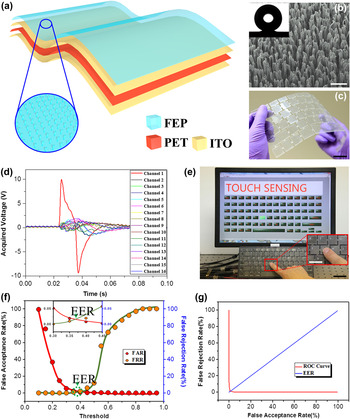
HMI is an effective way to convert human activities into electric output to command robot to detect the desired state by means of a biopotential system. With the contact electrification between human skin and PDMS, the output voltage and current density of the TENG device can, respectively, reach to 1000 V and 8 mA/m2, which indicated that it can also be applied as active sensors. Reference Yang, Zhang, Lin, Zhou, Jing, Su, Yang, Chen, Hu and Wang95 Furthermore, Chen et al. developed an intelligent keyboard (IKB), which can be used to guarantee the computers against unauthorized accessing. Reference Chen, Zhu, Yang, Jing, Bai, Yang, Qi, Su and Wang96 With a typical single-electrode TENG as the core component, IKB can transfer the type motions into electrical signals relying on the contact electrification between human finger and keys, which can identify personal typing signals that could be identified as personalized physiological data. As shown in Fig. 8(a), the key functional element of IKB is consisted of PET layer, ITO electrodes, and FEP layer. To enhance the effective contact area, nanowires array was purposely created on the FEP surface, as shown in Fig. 8(b). Furthermore, the FEP surface was intrinsically hydrophobic and with the increased surface roughness, the FEP surface becomes superhydrophobic and self-cleaning. Figure 8(c) demonstrated the photograph of an as-fabricated IKB equipped on a commercial keyboard. The IKB system can successfully convert the human typing motions into electrical signals. Each key on the IKB system was individually addressable by a multichannel measurement system. Figure 8(d) showed the output voltage signals from different channels. And the output voltage of the channel from each key striking can deliver a peak-to-peak value of 10 V. By signal processing via the Pauta criterion method and visualized by the LabView programming, the stroked key could display on the screen simultaneously without observable delay [Fig. 8(e)]. In addition, by using the collected personal typing patterns, two error rates, false rejection rate (FRR) and false acceptance rate (FAR), were used to evaluate the properties of the biometrics authentication system. FRR is the percentage of a genuine user rejected by the system incorrectly, while FAR is the probability of impostor inputs accepted incorrectly. Figure 8(f) chooses Pearson correlation coefficient as the classification threshold to evaluate the behavioral biometric authentication system. With the increase of threshold, FRR was elevating while FAR becomes decreasing, and their intersection represented the equal error rate (EER) point. In contrast with the traditional technology, the biometric authentication system obtained an obviously lower EER value of 1.34% at the threshold of 0.37. In the meanwhile, Fig. 8(g) indicated the receiver operating characteristic (ROC) curve of the biometric authentication system.
Personalized keystroke dynamics for self-powered human-machine interfacing: (a) schematic illustrations of the key functional element and inset shows an enlarged schematic of FEP nanowires on the top surface; it should be noted that these drawings are not to scale; (b) SEM image of FEP nanowires and inset shows contour of the resting droplet for surface static contact angle measurement (the scale bar is 500 nm); (c) photograph of a flexible and transparent key functional element (the scale bar is 3 cm); (d) the system acquired output voltage signals when the key “T” was stroked; (e) a photograph demonstrating the IKB for real-time keystroke tracing and recording (the scale bar is 5 cm) and inset shows an enlarged view of the key “G” being stroked (the scale bar is 2 cm); (f) evaluation of the performance of the biometric authentication system using triboelectrification enabled keystroke dynamics; the variation of FAR and FRR is related to the threshold. Inset: an enlarged view of the EER point; (g) receiver operating characteristic (ROC) curve of the biometric authentication system using triboelectrification enabled keystroke dynamics. Reproduced with permission from the American Chemical Society. Reference Chen, Zhu, Yang, Jing, Bai, Yang, Qi, Su and Wang96

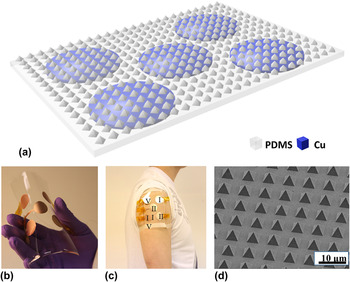
Regarding TENG based motion sensor for HMI, Yang et al. Reference Yang, Chen, Wen, Jing, Yang, Su, Zhu, Wu and Wang97 presented a motion sensor fabricated with flexible, recyclable, skin-friendly materials to track human muscle motion. As illustrated in Fig. 9(a), five separated flexible biopotential electrodes were made up to form the self-powered motion sensor. And the PDMS film, as the fabricating material, was patterned with micropyramids with an edge length of 4 μm, as shown in Fig. 9(d). Figures 9(b) and 9(c), respectively, demonstrated an as-fabricated motion sensor array and the one fixed on the surface of a shoulder joint. Owing to its independence, addressability, and self-powering, the motion sensor has used to record electric output signals, which can precisely quantify the freedom degrees, positions, and capacities of muscle motions. With an excellent signal-to-noise ratio of 1000, the output current density and voltage generated by motion sensor arrays can reach up to 10.71 mA/m2 and 42.6 V. Therefore, the device can serve as a motion sensor to precisely record and convert the motions of human joints, such as elbow, knee, heel, and even fingers, and thus distinguish it as a superior and unique invention in the field of HMI.
Triboelectrification based motion sensor for human-machine interfacing: a sketch (a) and photographs (b and c) of motion sensor array; (d) SEM image of the patterned PDMS film with pyramids features. Reproduced with permission from the American Chemical Society. Reference Yang, Chen, Wen, Jing, Yang, Su, Zhu, Wu and Wang97

VII. TENG AS A CHEMICAL SENSOR
The material surface of the triboelectric layers of the TENG is highly related to the device electrical signal output. While it is effective to modify the triboelectric surface with some chemical species or alternating chemical elements, and thus it could be developed into self-powered active chemical sensors for such as ion concentration and UV illumination detection.
The first work of TENG based chemical sensing was reported by Lin et al. Reference Lin, Zhu, Zhou, Yang, Bai, Chen and Wang98 And it showed the feasibility of ambient Hg2+ ions detection. By using a TENG in a vertical contact-separation mode, Au nanoparticles (NPs) were fixed on the metal slice to increase the effective contact area. Furthermore, 3-mercaptopropionic acid (3-MPa) molecules were used to modify the NPs to strengthen the Au–S interactions. Then, the gap between the triboelectric polarity of AuNPs and Hg2+ ions makes feasible the Hg2+ ions detection. Based on the rational design, the electrical output of TENG achieved up to 105 V in voltage and 63 μA in current with a device dimension of 1 × 1 cm. With a detection limitation of 30 nM, the reported nanosensor holds a linear range from 100 nM to 5 μM for ambient Hg2+ ions detection.
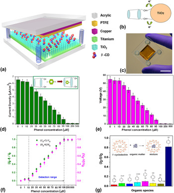
Moreover, Li et al. Reference Li, Chen, Yang, Su, Fan, Wu, Yu and Wang99 brought the conception to an application for self-powered phenol detection and electrochemical degradation. In this work, β-cyclodextrin (β-CD) was selected both as a surface modification chemical to enhance the TENG electrical output and also as the recognition element for phenol molecules detection. As shown in Fig. 10(a), acrylic was used as the structural supporting backbone of the device, which has a multilayered structure. PTFE thin film was used as the triboelectric layer with back-coated copper as the electrode. β-CD was packaged onto the TiO2 nanowires as the surface modified component. Figure 10(b) demonstrated the charge transfer between β-CD and TiO2. Figure 10(c) shows a TENG with β-CD surface modification with a dimension of 4 × 4 cm. The performance of the TENG based phenol sensor was measured via dropping different concentrations of phenol solutions onto the device. Figures 10(d) and 10(e), respectively, showed the dependence of short-circuit current density J sc and open circuit voltage V oc on different phenol concentrations, which both declined with the increasing of the phenol concentration within a range from 10 μM to 100 μM. The decay of the electric output was largely because of a modified surface triboelectric behavior, and phenol would replace the position of TiO2 to contact with PTFE. As shown in Fig. 10(f), the relative variation of output voltage and current with phenol concentrations indicated that a sensitivity of 0.02 μM−1 was obtained. Furthermore, control experiments were carried out to evaluate the selectivity of phenol sensors as compared with other organic species, as shown in Fig. 10(g). With a constant concentration of 50 μM for all the organic species, the output performance of phenol was larger than all the other organic species, which indicated an outstanding selectivity of the sensor for phenol detection. In addition, a further step was taken to electrochemically degrade the phenol in a self-powered manner in a large container, owing to the high electrical output performance of the TENG. This work paved a new and efficient pathway for the detection and degradation of the environmental chemical waste, which represented a solid advancement in the fields of wastewater treatment, ecological sanitation, environmental assessment, monitoring, and sustainability.
β-Cyclodextrin (β-CD) improved TENG for self-powered phenol detection and electrochemical degradation: (a) a sketch of the TENG with β-CD surface modification for phenol detection; (b) schematic diagram for illustrating the charge transfer from the hydroxyl groups of β-CD to TiO2 nanowires; (c) a photograph of the as-fabricated device for phenol detection (the scale bar is 2 cm); (d and e) under a fixed 80 μM β-CD surface modification, dependence of the current (d) and voltage (e) output on the phenol concentrations; (f) the sensitivity and detection range of the as-developed β-CD enhanced TENG for phenol detection in terms of both current and voltage output; (g) the selectivity of the as-developed β-CD enhanced TENG for phenol detection; the inset shows an illustration of the reaction mechanism between β-CD and different types of organic species. Reproduced with permission from the Royal Society of Chemistry. Reference Li, Chen, Yang, Su, Fan, Wu, Yu and Wang99

VIII. TENG AS POWER SOURCE FOR SELF-POWERED SENSING SYSTEM
A rapid development of personal electronics and sensor networks was to some extent hindered by the need of portable and sustainable power sources, which are now mostly relying on batteries. For batteries, the limited lifetime and potential environmental detriment makes them unfavorable for sensor network with large node population and wide-range distribution. Integrating miniaturized energy-harvesting device into the sensor system to realize the self-powered operation would be a superior solution.
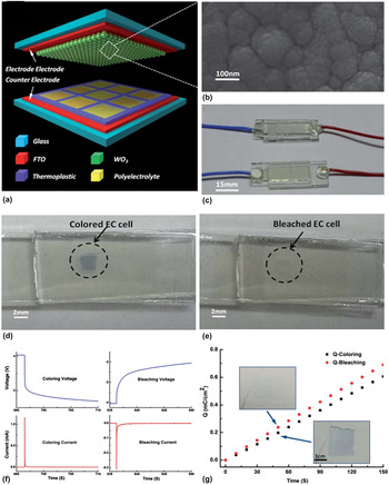
Electrochromic (EC) devices are able to change the optic performance reversibly through electrons injection and extraction powered by the applied potential in the external circuit. Yang et al. Reference Yang, Zhu, Wang, Zhang, Lin, Wu and Wang100 demonstrated a self-powered electrochromic device powered by a TENG. As shown in Fig. 11(a), an EC cell consists of multiple layers. The outer ones served as electrodes are glass coated with FTO, and between the two electrodes is a of WO3 layer with a thickness of about 250 nm [Fig. 11(b)] and polyelectrolyte. From the photograph of Fig. 11(c), we can see that the completely encapsulated EC devices have a transmittance even over 70%. In the discharging process, the voltage across the EC device and the current flowing through it were simultaneously monitored, with the results presented in Fig. 11(f) (left section). The current climbs to the highest point and then drops sharply with the capacitor continuous discharging, at the same time the device becomes dark in Fig. 11(d), which means the EC unit starts the process of coloring. Oppositely, voltage and current of the device [right section of Fig. 11(f)] are reversible and the EC unit gains the transmittance again [Fig. 11(e)], when the EC unit was reversely connected. Due to the increasing resistances of charge transfer from Li+ ions flowing into the WO3 film, the EC cell’s voltage also increases, which was continuously driven by a TENG. As shown in Fig. 11(g), the EC device finally switches from coloring to bleaching constantly with a clearly observable difference in ΔT vis. The reported self-powered EC system can be applied in monochrome displays or electronic billboards.
A self-powered electrochromic (EC) device driven by a TENG: (a) schematic structure of the WO3-based EC device; (b) SEM image of the WO3 film; (c) photographs of the EC device; (d) optical image of the colored EC; (e) the optical image of the bleached EC; (f) I t and V t of coloring (left pair) and bleaching processes (right pair); (g) the transmittance spectra of the EC in as-fabricated, colored, and bleached states. Reproduced with permission from the Royal Society of Chemistry. Reference Yang, Zhu, Wang, Zhang, Lin, Wu and Wang100

As known, the characteristics of human biomechanical motions are fluctuant in amplitudes and variable in low frequencies. Recently, Niu et al. Reference Niu, Wang, Yi, Zhou and Wang101 reported an effective self-powered system by harvesting human biomechanical energy as active sensors. Basically, the system consists of a high-output TENG, a manipulation of the circuit to transfer the chaotic biomechanical energy into power at an efficiency of 60%. For the energy-harvesting part, Kapton was structured into a zigzag shape by 10–15 layers. In every layer, the thin Al foil was acting as one electrode and the copper back-coated onto FEP was the other electrode [Fig. 12(a)]. And the as-fabricated TENG has small volume and was lightweight [Fig. 12(b)]. Figures 12(c) and 12(d), respectively, show that the voltage and the charge output can reach up to 700 V and 2.2 μC when the TENG was packaged into shoes to harvest energy from human walking. A systematically structural optimization could assure that all individual parts can operate collaboratively. Additionally, the total energy efficiency can reach up to 60% after solving the puzzle of impedance mismatch by using a designed power management circuit, which greatly enhanced the efficiency approximately two orders compared with that of the direct charging. By capturing power from human motions, the self-powered sensing system can be applied in many areas. As demonstrated in [Figs. 12(e) and 12(f)], respectively, a commercial thermometer and a scientific calculator were sustainably driven by the power supplying system.
Self-charging system for sustainable operation of mobile electronics: (a) structure of the designed multilayer TENG; (b) photograph of an as-fabricated TENG; (c) short-circuit current output and (d) open-circuit voltage output of the as-fabricated TENG; (e) demonstration of a self-powered temperature sensor; (f) demonstration of a self-powered scientific calculator. Reproduced with permission from the Nature Publishing Group. Reference Niu, Wang, Yi, Zhou and Wang101

IX. CONCLUSION AND FUTURE WORK
As the rapid advancement of modern technologies, mobile and portable sensor systems with applications in communication, personal healthcare, and environmental monitoring contributed largely to construct a world of better life. Power supplying to the sensor nodes in the network with large population and wide-range distribution could be a challenge. Self-powered smart sensors based on TENGs without external power sources could be of wide-range interest in many fields. On one hand, the environmental energies harvested by the TENG could provide sustainable electrical power to drive the mobile electronics and sensor networks. On the other hand, the electrical current and voltage signals generated by the TENG represent the dynamic and static variation corresponding to the change of mechanical motions or other environmental factors. It provides a superior solution for constructing active sensors without the need of external power sources. Various applications have been successfully demonstrated in the areas of micro-electromechanical systems, HMI, touching technology, security systems, and human-motion sensing.
With the introduction of new materials and surface engineering technologies, both the efficiency of TENG as a power source and sensitivity of TENG as active sensors are expected to be significantly improved. As moving toward the future applications of TENGs, several main issues and problems still need to be well addressed. Reference Chen102,Reference Chen and Wang103 First, since the TENG output performance is highly subjected to environmental factors, such as temperature, humidity, pressure, particle contaminations and so on. Effective packaging technology of the TENG unit is vitally important to make commercialized products, especially for application in a variety of hash environments. Effects should be devoted to take care of possible air gaps due to the motion part without affecting its sensitivity. Second, the durability and output stability of the device can be improved from both materials usage and the device design. Third, based on the surface charging effect, the TENG based sensing application is also challenged when the device dimension is miniaturized, which greatly hinders its further development into the micro-electromechanical systems. More advanced device design and fabrication techniques are highly desired to accomplish a higher spatial resolution of the TENG based active sensors.
In summary, this article gives a comprehensive review of the recent progress for TENG based self-powered active sensing. The tremendous developments in this field could lead a revolution to our way of life, although this may be a long-term goal.
ACKNOWLEDGMENTS
This work was sponsored by the Program for New Century Excellent Talents in University of China (NCET-13-0631) and the Fundamental Research Funds for the Central Universities (106112016CDJZR225514). The authors also thank Professor Zhong Lin Wang and his group at Georgia Institute of Technology for the pioneering work on triboelectric nanogenerators and self-powered sensing systems.