Introduction
High-voltage gallium nitride (GaN)-based power switching transistors enable efficient power converters with increased power density. High converter switching frequencies can be realized with lateral GaN-based heterostructure field-effect transistors (HFETs) due to the low area-specific ON-state resistance for a given maximum voltage than can be applied to the transistor in the OFF-state (blocking voltage) and the low-gate charge required for switching. GaN-HFET technology is also considered to be cost-efficient since devices can be manufactured on six-inch (150-mm) and eight-inch (200-mm) Si substrates using existing complementary metal oxide semiconductor (CMOS)-fabrication processing.Reference Moens, Liu, Banerjee, Vanmeerbeek, Coppens, Ziad, Constant, Li, De Vleeschouwer, RoigGuitart, Gassot, Bauwens, De Backer, Padmanabhan, Salih, Parsey and Tack1,Reference De Jaeger, Van Hove, Wellekens, Kang, Liang, Mannaert, Geens and Decoutere2 While radio frequency GaN HFETs on SiC substrates are considered mature, power switching applications are migrating to GaN-on-Si due to reasons of substrate costs and diameters, as well as compatibility with existing Si-device production lines. However, the lattice mismatch and thermal expansion coefficient mismatch between Si and GaN are larger than those between SiC and GaN. Growing high-quality GaN layers on Si substrates is therefore quite a challenge.Reference Ikeda, Niiyama, Kambayashi, Sato, Nomura, Kato and Yoshida3 Differences in substrate electrical and thermal conductivities may also impact device performance.
Lateral GaN-HEMTs use a highly conductive thin electron layer established at the heterojunction between the GaN-buffer layer and the AlGaN-barrier layer as the transistor channel (inset of Figure 1) known as a two-dimensional electron gas (2DEG). These devices have intrinsic normally ON properties since the transistor gate needs to be negatively biased to deplete the transistor channel. However, a normally OFF characteristic is required for power electronics applications due to inherent safety concerns. Only then can unwanted power flow be suppressed in the case where there is no control voltage on the transistor gate. The realization of robust normally OFF device technology is a major challenge for GaN switching transistor maturity in power electronic applications.
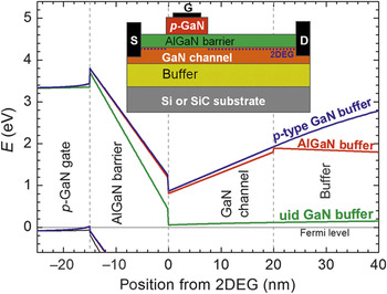
Simulated band diagram at the gate position of a p-GaN gate Al0.23Ga0.77N/GaN heterostructure field-effect transistor for different buffer compositions: unintentionally doped (uid) GaN buffer in green; Al0.05Ga0.95N buffer in red; and p-type GaN buffer in blue. The conduction band energy (E) at the two-dimensional electron gas (2DEG) position is significantly shifted above the Fermi level for the AlGaN buffer or p-type GaN buffer structure. Inset: Schematic cross-section of the heterostructure field-effect transistor. The GaN or AlGaN-based buffer layers the GaN channel, and the AlGaN barriers are grown with heteroepitaxy on top of a SiC or Si substrate. Source (S) and drain (D) are electrically connected by the 2DEG blue dotted line that is interrupted beneath the p-type gate (G). Adapted from Reference 16.

The observed increased dynamic ON-state resistance (R ON) when switching the GaN-transistor from the high-voltage OFF-state bias to ON-state is an additional challenge for high-voltage GaN devices, since it generates additional unwanted losses a short time after switching and reduction of the increased. High internal electric fields combined with high GaN material dislocation densities lead to device charging when applying high OFF-state drain voltages on the order of several 100 V. The resulting increased dynamic ON-state resistanceReference Ikeda, Niiyama, Kambayashi, Sato, Nomura, Kato and Yoshida3 generates additional ON-state losses for switching applications and may compromise the principal advantages of GaN-based switches as compared to Si-based devices.
A normally OFF p-GaN gate GaN HFET for the 600 V class used in the majority of 230 V mains supply applications is introduced in the next section, and its static and dynamic properties are compared with Si-based superjunction metal oxide semiconductor field-effect transistors (MOSFETs) that have a particular low ON-resistance of the drift layer due to charge compensation doping.Reference Deboy, März, Stengl, Strack, Tihanyi and Weber4 This device class is currently considered as state of the art for fast 600 V switching transistors. The subsequent sections deal with specific device technology topics, including the gate module used for the normally OFF characteristic, GaN buffer compositions that promote high-blocking voltage, and the impact of the buffer properties on the dynamic ON-state resistance. In the discussions, emphasis is placed on comparing transistors built on SiC or silicon substrates.
State-of-the-art switching transistor
Normally-OFF GaN switching transistors (70 mΩ/600 V) have been produced on 3-inch (75-mm) and 4-inch (100-mm) wafers, with the GaN layers grown by metal–organic chemical vapor deposition (MOCVD) on either SiC substrates or Si substrates with the same device layout.Reference Hilt, Zhytnytska, Böcker, Bahat-Treidel, Brunner, Knauer, Dieckerhoff and Würfl5 An iron-doped GaN buffer (GaN:Fe) was used for the GaN-on-SiC devices to compensate for the n-type nature of MOCVD-grown GaN layers.Reference Hilt, Kotara, Brunner, Knauer, Zhytnytska and Würfl6 The GaN-on-Si HFET structure was grown by the company EpiGaN.7 Gates with a 214 mm width were arranged on a 4.4 × 2.3 mm2 chip.
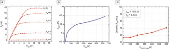
The output characteristics of a GaN-on-SiC power transistor (Figure 2a) show a maximum saturated pulse current of 117 A for ON-state conditions (V GS = 5 V).Reference Hilt, Zhytnytska, Böcker, Bahat-Treidel, Brunner, Knauer, Dieckerhoff and Würfl5 The ON-state resistance is 65 mΩ or less. The transistor is closed at V GS = 1 V or less. In the OFF-state, the drain leakage increases up to 100 µA for 600 V drain bias (Figure 2b). The dynamic R ON is increased by a factor of 1.25 as measured 2.5 µs after switching from a 600 V OFF-state to 5 A ON-state (Figure 2c). Such a device would generate ON-state losses of 33 W and OFF-state losses of 60 mW when used for switching 20 A and 600 V at 100 kHz in a simple voltage down-converting buck-converter with 2–3 kW output power. Here, the increased dynamic R ON was already taken into account.
Direct current and pulsed characteristics of a 70 mΩ/600 V GaN transistor in GaN-on-SiC technology with 214-mm gate width. (a) The output characteristic (gate bias V GS indicated) shows a 117 A pulse current (I D) in the ON-state at V GS = 5 V. The device is closed at V GS = 1 V. (b) The OFF-state leakage current (I DOFF) is limited to 100 µA for a 600 V drain bias (V DS). (c) The increase of the dynamic ON-state resistance (R ON), depending on the OFF-state voltage (V DSOFF-state). The time of applied V DSOFF-state (t OFF) and the elapsed time after switching into ON-state (t ON) have strong impact on the dynamic R ON. Adapted from Reference 5.

The chip-area specific ON-state resistance is as low as R ON × A = 0.66 Ωmm2. Here, A is the full chip area. A smaller chip area is required for this GaN transistor compared to similarly rated 600 V Si-based superjunction MOSFETs, featuring typically R ON × A = 1–2 Ωmm2. Efficient use of the (expensive) chip area is thus demonstrated despite the GaN transistor lateral design that usually consumes more chip area as compared to the vertical design used for Si MOSFETs.
GaN-on-Si transistors with the same device layout produced very similar processing modules, which yielded a 92 A maximum saturated pulse current and 70 mΩ ON-state resistance.Reference Hilt, Zhytnytska, Böcker, Bahat-Treidel, Brunner, Knauer, Dieckerhoff and Würfl5 The lower current and higher R ON for the GaN-on-Si devices as compared to the GaN-on-SiC devices correlates well with the 20% difference of the 2DEG sheet resistance in-between the wafers used. The respective transfer characteristics are analyzed in the next section.
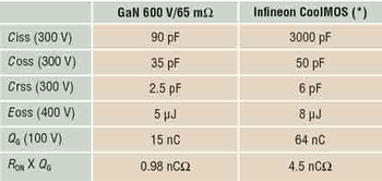
The capacitances inside the transistor mainly determine the charges needed to transfer the device from the OFF-state (with high-drain bias) to the ON-state and vice versa. This combined shifting of drain voltage and charge during the switching events produces device switching losses. Due to the unipolar nature of the GaN HFET and the lateral design, capacitances are very low (Table I). The associated switching energy of Eoss = 5 µJ is less than that for a state-of-the-art Si-based superjunction MOSFET with similar R ON and blocking voltage rating.
Comparison of essential dynamic transistor parameters between the 70 mΩ/600 V normally OFF GaN transistor (with SiC substrate) and a commercial state-of-the-art Si-based superjunction metal oxide semiconductor field-effect transistor.

(*) 650 V/70 mΩ C7 CoolMOS in thinPAK Infineon IPL65R070C7.
Adapted from Reference 5. Note: Ciss, input capacitance; Coss: output capacitance; Crss: reverse capacitance; Eoss, switching energy, Q G, gate charge; R ON, ON resistance.
The switching speed and efficiency of transistors is often limited by the gate charge Q G needed for switching from the OFF-state to the ON-state. To cancel out the influence of transistor size and gate width, the product R ON × Q G is often taken as an important benchmark for the switching speed and efficiency. Here, the GaN transistor technology with R ON × Q G = 1 nCΩ requires less than a quarter of the gate charge of a comparable Si-based superjunction MOSFET (Table I). In conclusion, the 70 mΩ/600 V normally OFF GaN transistor described here features a high-pulse current with a small footprint combined with low gate charge and capacitances.Reference Hilt, Zhytnytska, Böcker, Bahat-Treidel, Brunner, Knauer, Dieckerhoff and Würfl5
Technology for normally OFF GaN HFETs
Recent attempts to convert AlGaN/GaN HEMTs into normally OFF devices used gate-recess,Reference Saito, Takada, Kuraguchi, Tsuda and Omura8 where the AlGaN barrier was thinned down beneath the gate to remove 2DEG, or fluorine-incorporationReference Cai, Zhou, Lau and Chen9 into the AlGaN barrier beneath the gate to deplete 2DEG. These approaches limited applicability for power electronics due to their low threshold voltages V th < +1 V, a low gate bias separation of ∼2 V between OFF and ON-state (gate swing), and high ON-state gate current. The introduction of a gate insulator suppresses the gate current and may extend the gate swing.Reference Moens, Liu, Banerjee, Vanmeerbeek, Coppens, Ziad, Constant, Li, De Vleeschouwer, RoigGuitart, Gassot, Bauwens, De Backer, Padmanabhan, Salih, Parsey and Tack1,Reference De Jaeger, Van Hove, Wellekens, Kang, Liang, Mannaert, Geens and Decoutere2 The extrinsic insulator layers are often atomic layer deposition-based oxides such as Al2O3 or HfO2 and are deposited at temperatures <300°C. The observed trap states in the insulator bulk or at the interface to the AlGaN barrier often deteriorate the device switching performance and limit device reliability.Reference Sun, Saadat, Chang-Liao, Palacios, Cui and Ma10
Normally OFF behavior can also be obtained by connecting the drain of a normally OFF standard Si transistor optimized for low voltage operation to the source of a high-voltage GaN normally ON transistor with a grounded gate inside one package (cascode configuration).Reference Liu, Huang, Lee and Li11 From outside the package, the device appears as a high-voltage normally OFF transistor that has the advantage of large gate threshold voltage and gate voltage swing (feature of the Si normally OFF transistor), a high-breakdown voltage, and a comparably low ON-state resistance as a consequence of the GaN HFET. The disadvantage is that the GaN HFET cannot be driven to a full ON-state condition, which would need a positive gate bias. Moreover, the input capacitance is increased by the Si-MOSFET, and the parasitic inductances of the additional wiring increases the switching losses.Reference Liu, Huang, Lee and Li11
p-GaN gate technology
In the p-GaN gate transistors presented here, the gate consists of in situ grown Mg-doped GaN with an ohmic contact for biasing (Figure 1).Reference Hilt, Knauer, Brunner, Bahat-Treidel and Würfl12p-GaN gate HFETs combine the high-mobility 2DEG transistor channel known from AlGaN/GaN HEMTs with robust normally OFF operation with a 1–2 V threshold voltage, as required for applications in power electronics.Reference Hilt, Knauer, Brunner, Bahat-Treidel and Würfl12,Reference Uemoto, Hikita, Ueno, Matsuo, Ishida, Yanagihara, Ueda, Tanaka and Ueda13 Researchers at Samsung were able to shift the threshold voltage up to V th = 4 V by introducing a Schottky-type contact to the p-GaN gate.Reference Hwang, Kim, Choi, Choi, Lee, Kim, Park, Lee, Ha, Oh, Shin and Chung14 Similar to enhancement-mode GaN metal insulator semiconductor field-effect transistors, a wide gate swing allows secure ON-state and OFF-state conditions, even in applications with high electromagnetic interference noise.
When unbiased, the p-type gate depletes the 2DEG of the transistor channel, and a positive gate bias is needed to open the transistor. The simulated band diagram at the gate position (see Figure 1) confirms that the 2DEG channel at the heterojunction between the GaN buffer and AlGaN barrier does not cross the Fermi level (green conduction band line in Figure 1). Replacing the GaN-buffer with an AlGaN buffer and using unintentionally doped (uid) GaN for the transistor channel generates virtual p-type doping at the AlGaN back-barrier of the channel.Reference Bahat-Treidel, Hilt, Brunner, Würfl and Tränkle15 The potential well of the 2DEG is then dragged above the Fermi level by almost 1 eV (red conduction band line in Figure 1) and a more positive gate bias is required to again fill the 2DEG channel beneath the gate. Using an AlGaN-buffer structure is thus beneficial for a high threshold voltage. A similar high energy of the heterojunction potential well can be obtained by a GaN-buffer with p-type properties (blue conduction band line in Figure 1) beneath the uid GaN-channel.
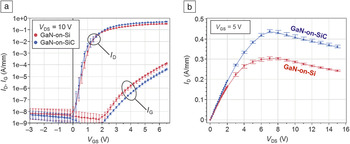
Fabricated p-GaN gate transistors based on an Al0.05Ga0.95N buffer, carbon-doped GaN buffer (GaN:C), and an iron-doped buffer (GaN:Fe) have demonstrated that the predicted normally OFF characteristics are valid for the different buffer compositions.Reference Hilt, Bahat-Treidel, Brunner, Knauer, Zhytnytska, Kotara and Würfl16 The logarithmic representation of the transfer characteristics (Figure 3a) show that a secure normally OFF characteristic can be realized on both SiC and Si substrates. These results are from devices with a 3.2 mm gate width that originates from the same wafers as the transistor presented earlier with 70 mΩ ON resistance (Figure 2). Threshold voltage (V th = 1.1 V), sub-threshold drain current, OFF-state drain leakage (10 nA/mm for 0 V gate bias), and ON-state gate current (4–10 µA/mm for 5 V gate bias) are almost identical for both substrate types. In the ON-state, the gate bias can be driven up to 6 V and higher, but the gate current increases due to the pin-diode-like nature of the gate module. The gate bias for the ON-state condition should be V GS = 5 V in order to limit the ON-state gate current to approximately 10 µA/mm.
(a) Transfer characteristics and gate current (I G) and (b) ON-state I-V curve of p-GaN gate heterostructure field-effect transistors realized in GaN-on-SiC (blue) or GaN-on-Si (red) technology. The median currents with quantiles of 30 devices spread over a 3-inch (75 mm) wafer are shown. Device gate width is 3.2 mm; gate-drain separation is 15 µm. Threshold voltage OFF-state leakage and ON-state gate current and ON-state resistance are similar for both substrate types but maximum drain current differs significantly. Note: I D, drain current; V DS, drain bias; V GS, gate bias. Adapted from Reference 5.

Significant differences between the substrate types can be found for high power operation. The 2DEG sheet resistance of the GaN-on-Si wafer is 20% higher than that for the GaN-on-SiC wafer. A proportional ratio is thus expected for the transistor ON-state resistance and the inverse of the maximum drain current in-between these wafers. From Figure 3b, R ON (measured at low power dissipation) is 18% higher for the GaN-on-Si devices as compared to the GaN-on-SiC devices, but the maximum drain current of the GaN-on-Si devices (I DSmax = 0.3 A/mm at V DS = 7.5 V) is only 68% of the current of the GaN-on-SiC devices. The low I DSmax of the GaN-on-Si devices can be understood by the increased channel temperature of GaN-on-Si transistor cells when an electric power of 7 W or greater is dissipated on an active device area of 0.1 mm.Reference De Jaeger, Van Hove, Wellekens, Kang, Liang, Mannaert, Geens and Decoutere2 Here, SiC, with its three times higher thermal conductivity compared to Si, has better potential to remove heat from the active device region.
Transistor blocking voltage
High electrical breakdown strength of the semiconductor material is of double benefit for lateral switching transistors since it allows a reduced gate-drain separation for a given transistor blocking voltage. R ON for a given chip size is then reduced due to the shorter source-drain distance and due to the larger gate width on the chip area. The breakdown strength of GaN (∼3.3 MV/cm) is approximately 10 times higher than for silicon.
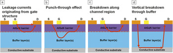
Careful design of the electrical field distribution inside the semiconductor layers is required to fully benefit from these material properties. Figure 4 compiles some possible leakage scenarios, where versions (a), (b), and (c) limit lateral blocking voltage, while the leakage path (d) limits vertical blocking.
Collection of four mechanisms limiting high-voltage capability of GaN heterostructure field-effect transistors. (a) Leakage currents originating from gate structure; (b) punch through effect; (c) breakdown along the channel region; and (d) vertical breakdown through the buffer. The red arrows show the principal path of electron leakage current through the device that limits the transistor blocking voltage. Adapted from Reference 21. Note: D, drain; G, gate; S, source.

Lateral blocking
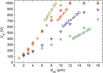
The breakdown voltage of GaN HFETs should ideally increase with the gate-drain separation d GD according to leakage path (c) in Figure 4. This breakdown voltage scaling is reduced or lost when gate leakage becomes significant (Figure 4a) or the electrons from the transistor channel bypass the gate control region via deep layers in the buffer (Figure 4b). The major cause for case (b) is the limited barrier height of the GaN buffer beneath the transistor channel with the 2DEG.Reference Bahat-Treidel, Hilt, Brunner, Würfl and Tränkle15 Better electron confinement to the channel to suppress the leakage path (b) can be realized by either an AlGaN back barrier or by p-type compensation doping of the buffer beneath the GaN channel, as shown by the buffer conduction band rising in Figure 1 (red and blue lines).Reference Hilt, Bahat-Treidel, Brunner, Knauer, Zhytnytska, Kotara and Würfl16
Several GaN buffer compositions grown on n-type (conductive) SiC substrates have been examined to yield sufficient transistor blocking with a magnitude of up to one-third of the material breakdown strength (Figure 5).Reference Hilt, Bahat-Treidel, Brunner, Knauer, Zhytnytska, Kotara and Würfl16 A breakdown voltage scaling of ∼40 V/µm gate-drain separation was measured for Al0.05Ga0.95N back-barrier based p-GaN gate devices, and a 700 V breakdown voltage was obtained. GaN-buffer compensation doping was realized with carbon (GaN:C) or iron (GaN:Fe). More than a 1000 V breakdown strength with 110 V/µm scaling has been obtained for GaN:C-based p-GaN gate transistors. Transistors based on a GaN:Fe buffer yield 50–60 V/µm breakdown strength scaling. A GaN buffer grown on a silicon substrate from an external vendor (GaN-on-Si) also shows a high breakdown strength of 80–90 V/µm, with a characteristic similar to the carbon-doped GaN buffer grown on SiC substrate.Reference Hilt, Zhytnytska, Böcker, Bahat-Treidel, Brunner, Knauer, Dieckerhoff and Würfl5,Reference Hilt, Bahat-Treidel, Brunner, Knauer, Zhytnytska, Kotara and Würfl16
Transistor breakdown voltage (V Br) as a function of gate-drain separation (d GD) for different buffer compositions. The substrate backside was kept electrically isolated (floating). Symbols are wafer medians. The upper drain bias (V DS) limit of the setup was 1000 V; some structures have in fact a higher breakdown voltage. Adapted from Reference 16.

Vertical blocking
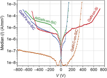
Sufficient vertical isolation of the GaN-based layers is required for a high transistor blocking voltage when conductive substrates are used. Compared to semi-insulating SiC, conductive substrates such as n-type SiC or Si offer a considerable cost advantage. Vertical leakage currents from a drain- or source-contact with a 300 µm diameter from the top of the GaN-based layers toward the grounded substrate are shown in Figure 6 for the same wafers as in Figure 5. There are particularly high vertical leakage currents for the AlGaN-buffer and GaN:Fe-buffer devices that would limit transistor blocking voltage to approximately 120 V only if the substrate is at source potential. A blocking voltage of 600 V can be achieved for a configuration with the substrate at drain potential or for a floating (electrically isolated) substrate. However, a source-connected substrate is preferred for many applications, since a drain-connected substrate would introduce an additional capacitance between the substrate and the (grounded) heat sink and generate additional switching losses.
Vertical leakage current (I) from a circular drain pad with a 300-µm diameter to the grounded conductive substrate as a function of vertical bias (V) for four different buffer types. The vertical leakage limits the transistor blocking voltage to ∼150 V for the GaN:Fe and AlGaN buffer structures, to ∼350 V for the GaN:C structure and to ∼700 for the GaN-on-Si structure if the substrate is kept at source potential. Wafer medians are shown. Adapted from Reference 16.

Approximately two orders of magnitude lower vertical leakage currents were measured for the structures based on a GaN:C buffer, and a 400 V blocking voltage can be obtained for the source-connected substrate. With a 700 V vertical blocking voltage, the GaN-on-Si structure shows the best isolation for the source-connected substrate configuration. Transistor switching operation in the source-connected substrate configuration was demonstrated up to 500 V.Reference Hilt, Zhytnytska, Böcker, Bahat-Treidel, Brunner, Knauer, Dieckerhoff and Würfl5 In conclusion, carbon-doped GaN buffer structures give significant advantages in terms of lateral and vertical blocking voltage as compared to the GaN:Fe and AlGaN buffer compositions.
Increased dynamic ON-state resistance
Besides the transistor OFF-state properties, the switching dynamics are also strongly determined by the buffer composition. An increase in the dynamic R ON immediately after switching from high-bias OFF-state condition is often observed in GaN-HFETs. Trap states in the (Al)GaN-based semiconductor stack or on the semiconductor surface are considered as the root cause for this effect.Reference Jin and del Alamo17 Electron traps inside the buffer or passivation layer may get filled under high-bias OFF-state conditions and deplete the transistor channel after switching the transistor to the ON-state since electron detrapping time constants are longer than the switching cycle time.
To analyze the increase of dynamic R ON pulsed ON-state, I-V curves have been measured with 65 V OFF-state drain voltage.Reference Hilt, Bahat-Treidel, Brunner, Knauer, Zhytnytska, Kotara and Würfl16 The pulse time in ON-state was 0.2 µs, and the time in OFF-state in between pulses was 2.5 ms. For all buffer compositions, a reduced current was obtained when switching from 65 V drain bias, as compared to switching from the non-stressed condition with 0 V drain bias.
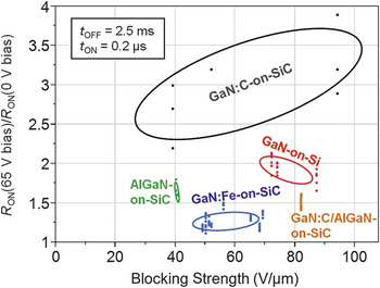
Figure 7 plots the increase in dynamic R ON, as measured from 65 V OFF-state bias in relation to the device blocking strength (V Br/d GD), as determined from Figure 5 and other wafers.Reference Hilt, Bahat-Treidel, Brunner, Knauer, Zhytnytska, Kotara and Würfl16,Reference Hilt, Bahat-Treidel, Cho, Singwald and Würfl18 It highlights the trade-offs between dispersion and blocking strength of different buffer compositions. Data were collected for GaN:C buffer devices with different carbon concentrations ranging from 1 × 1018 cm–3 to 4 × 1018 cm–3. Both blocking strength and dynamic R ON increase with carbon concentration. Even for the lowest carbon concentration, the increase in dynamic R ON (factor 2.5–3) is still unacceptably high when compared to other similar devices.Reference Hilt, Bahat-Treidel, Cho, Singwald and Würfl18
Increase in dynamic ON-state resistance (R ON) for t ON = 0.2 µs long pulses into ON-state from 65 V OFF-state bias (applied for t OFF = 2.5 ms) with respect to the non-stressed dynamic R ON (0 V gate bias) in relation to the device blocking strength scaling (see Figure 5). Test transistors with buffer types from Figures 5 and 6 with 0.25-mm gate width are compared. For the GaN:C buffer devices the carbon concentration is 1 × 1018 cm−3 to 4 × 1018 cm−3. The lowest dispersion was obtained for the GaN:Fe-on-SiC structure, but this buffer structure has a trade-off in blocking strength. The GaN-on-Si structure shows a very high blocking strength but some increased dispersion. Adapted from References 6 and 16.

The GaN:C/AlGaN-on-SiC structure gives the best combined performance with low dispersion and high blocking strength and demonstrates that strong dispersion due to buffer carbon doping can be avoided.Reference Hilt, Bahat-Treidel, Brunner, Knauer, Zhytnytska, Kotara and Würfl16,Reference Uren, Silvestri, Cäsar, Hurkx, Croon, Šonský and Kuball19 The lowest dispersion was obtained for the GaN:Fe-on-SiC structure, but this buffer structure has a trade-off in blocking strength. The GaN-on-Si structure shows a very high blocking strength but some increased dispersion.
The dynamic R ON of the packaged GaN-on-SiC transistor with 214 mm gate width for higher OFF-state voltages (Figure 2c) was determined from pulsed I-V curves where the OFF-state bias was applied for 1 ms and the I-V data were taken after 2 µs in ON-state (Figure 2c).The dynamic R ON for the GaN-on-SiC device continuously increases with the OFF-state bias up to a factor of 1.25 for 600 V switching (Figure 2c). This transistor uses the same iron-doped GaN buffer structure as the GaN:Fe samples shown in Figure 7. Different data for the dynamic R ON increase are obtained due to differences in the OFF-state voltage, the OFF-state time (t OFF) and the ON-state time (t ON).Reference Jin and del Alamo17,Reference Tanaka, Ishida, Ueda and Tanaka20
Summary
A normally OFF 70 mΩ/600 V GaN switching power transistor with high pulse currents on a small footprint combined with low gate charge and low capacitances was described. The device outperforms Si-based superjunction MOSFETs in terms of gate charge and switching energy. The p-GaN gate module for the normally OFF characteristic can be used on devices based on SiC substrates as well as on Si substrates.
The GaN buffer composition has a strong impact on several key parameters, such as the threshold voltage, the lateral and vertical blocking voltage, and the device dispersion. Suitable buffer structures are able to overcome the often observed trade-off between either high-blocking voltage or low dynamic ON-state resistance.
Using a Si substrate yields big challenges for the vertical blocking voltage and minor trade-offs in the static and the dynamic ON-state resistance. The high thermal impedance of devices on silicon can further increase the effective R ON under high-power conditions.
Acknowledgments
We are grateful to J. Böcker and S. Dieckerhoff from Technical University Berlin for discussions regarding high-current device characterization, support from the German BMBF (LES project PowerGaNPlus, contract no. 13N10908), and from EU FP7 project HipoSwitch (Grant no. 287602).