Introduction
Atomistic materials modeling has become a valuable tool in contemporary materials science. The accelerated characterization of known materials and the assessment of hypothetical systems are being supported by developments in software and hardware, including an international supercomputing infrastructure and a growing number of reliable simulation packages. Reference Lejaeghere, Björkman, Blaha, Blügel, Blum, Caliste, Castelli, Clark, Dal Corso, de Gironcoli, Deutsch, Dewhurst, Di Marco, Draxl, Dułak, Eriksson, Flores-Livas, Garrity, Genovese, Giannozzi, Giantomassi, Goedecker, Gonze, Grånäs, Gross, Gulans, Gygi, Hamann, Hasnip, Holzwarth, Iuşan, Jochym, Jollet, Jones, Kresse, Koepernik, Küçükbenli, Kvashnin, Locht, Lubeck, Marsman, Marzari, Nitzsche, Nordström, Ozaki, Paulatto, Pickard, Poelmans, Probert, Refson, Richter, Rignanese, Saha, Scheffler, Schlipf, Schwarz, Sharma, Tavazza, Thunström, Tkatchenko, Torrent, Vanderbilt, van Setten, Van Speybroeck, Wills, Yates, Zhang and Cottenier1 The predictive power of numerical simulation approaches, based on quantum mechanical description of solids, underpins the emerging field of computational materials design. Reference Butler, Frost, Skelton, Svane and Walsh2
While first-principles methodologies, for example, those based on density functional theory (DFT), were once limited to simple structures and compositions with tens of atoms in a crystallographic unit cell, modern computer architectures can support the direct simulation of thousands of atoms. The chemical and physical properties of metal–organic frameworks (MOFs) are now accessible to high-quality quantum mechanical simulations. In the past, simple empirical potentials proved useful for screening compositions and topologies in the context of gas storage. Reference Wilmer, Leaf, Lee, Farha, Hauser, Hupp and Snurr3 As interest in MOFs extends toward their physical properties and chemical reactivity, knowledge of the electronic structure becomes essential and crucial.
In this article, following a brief description of the common workflow for calculating the physical response functions of hybrid solids, we review recent progress in our understanding of the chemical bonding underpinning the electronic structure of MOFs. This includes the atomic and molecular orbitals that overlap to form the valence and conduction bands, the electron addition and removal energies, and a set of design principles for tailoring the electronic and optical activity for functional devices.
From computer to properties
Input: Crystal structure
A reliable structure is an essential starting point for quantum mechanical calculations of crystalline solids. The ground-state distribution of electrons is determined for a particular arrangement of ions in a lattice that extends infinitely across three spatial dimensions. The crystallography of MOFs is challenging: many reported structures contain solvent molecules, lattice sites with partial occupancy, or missing hydrogen atoms. In addition, high-symmetry space groups are usually assigned in the absence of hydrogen (due to their low electron density and weak diffraction intensity). The symmetry is often lowered when hydrogens are included, for example, when carbon atoms are replaced by the appropriate CH, CH2, or CH3 groups. One useful resource is the CoRE-MOF (computation-ready, experimental MOF) database 4 that provides “simulation ready” structures and has been employed in high-throughput screening projects. Reference Chung, Camp, Haranczyk, Sikora, Bury, Krungleviciute, Yildirim, Farha, Sholl and Snurr5
A further concern, which has not been fully explored for MOFs, is that Bragg diffraction provides insights into the (spatial and temporal) average crystal structure, but the local environment may be quite different. Reference Dove6 For organic–inorganic solids, there is the possibility of vibrations, librations, and rotations of atoms or molecular units. Reference Kieslich, Forse, Sun, Butler, Kumagai, Wu, Warren, Walsh, Grey and Cheetham7–Reference Brivio, Frost, Skelton, Jackson, Weber, Weller, Goñi, Leguy, Barnes and Walsh10 Structural disorder has been recognized as a potentially useful trait in framework materials, Reference Cairns and Goodwin11 but from the point of view of atomistic simulation of MOFs, it has been largely neglected up to this point.
Output: Physical properties
The crystal structures obtained from experiments are usually subject to local optimization for a chosen description of the interatomic interactions. The three lattice vectors and all lattice sites are minimized with respect to the external pressure and internal forces on the system. For a modern DFT exchange-correlation functional (e.g., PBEsol Reference Perdew, Ruzsinszky, Csonka, Vydrov, Scuseria, Constantin, Zhou and Burke12 ), experimental and measured structural parameters usually agree to within several percent.
On the United Kingdom supercomputer ARCHER (advanced research computing high-end resource), which is representative of the current generation of national systems, a high-quality electronic structure calculation of a MOF with several hundred atoms in the unit cell will require up to 48 h on 24 compute nodes (1152 cores). The high computational cost of performing a quantum mechanical calculation is balanced by the wealth of information that can be accessed, including structural, mechanical, magnetic, and optical properties. For example, heats of formation can be used to screen hypothetical compositions, Reference Hendon, Tiana, Vaid and Walsh13 the strength of electron-exchange interactions can be used to predict magnetic critical temperatures, Reference Svane, Saines and Walsh14 and the composition of frontier orbitals can be used to explain catalytic activity. Reference Nasalevich, Hendon, Santaclara, Svane, van der Linden, Veber, Fedin, Houtepen, van der Veen, Kapteijn, Walsh and Gascon15
Electronic structure: More than a sum of parts
A wide variety of MOFs have been reported with organic and inorganic networks ranging from zero to three dimensions of connectivity. Reference Cheetham, Rao and Feller16 For example, the hybrid halide perovskites that are being intensively studied for applications in solar-energy conversion can be considered as the combination of a three-dimensional (3D) anionic inorganic framework with a zero-dimensional (0D) cationic molecular sublattice. Reference Frost, Butler, Brivio, Hendon, van Schilfgaarde and Walsh17 For conciseness, we restrict our present discussion to standard porous MOFs with 3D inorganic–organic–inorganic connectivity (as found in the ubiquitous MOF-5 that combines a cationic zinc oxide subunit connected by anionic benzene dicarboxylate linkers to form a 3D porous framework [see Figure 1a, center]).
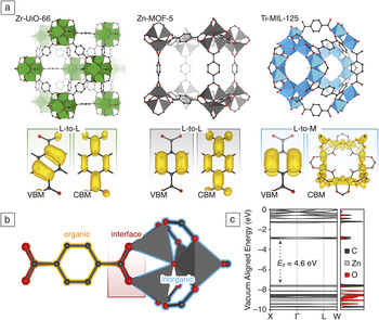
(a) Zr-UiO-66, Zn-MOF-5, and Ti-MIL-125 are metal–organic frameworks (MOFs) composed of closed-shell metal oxide clusters (M) linked by benzene dicarboxylate (L). Their topologies are varied and are determined by the geometry of the inorganic nodes (polyhedra colored green, black, and blue). (b) The electronic properties and frontier orbital compositions are determined by the interface of the inorganic and organic regions. The electron density isosurfaces are colored yellow. Most MOFs have poor electronic communication between neighboring motifs, resulting in electronic band structures with low dispersion, with charge-carrier localization. (c) The electronic band structure (density functional theory with HSE06 exchange and correlation) along the high symmetry lines of Zn-MOF-5 is presented with the atom-projected electronic density of states. Note: E g, bandgap energy; VBM, valence-band maximum; CBM, conduction-band minimum; MIL, Materials Institut Lavoisier; UiO, University of Oslo; X, Γ, and W refer to special k-points in the electronic Brillouin zone. Reference Butler, Hendon and Walsh46

The orbital composition and spatial location of the valence and conduction bands determines most equilibrium properties of materials. The electronic structure of most MOFs can be described in a manner similar to molecular orbital diagrams common to organometallic chemistry. However, the diverse chemistry of both the organic linkers and the inorganic nodes—for example, whether the node includes an inorganic cation like the Zn4O6+ cluster of the isoreticular (IRMOF) series—can require more detailed considerations. In particular, interesting chemistry occurs at the inorganic–organic interface. While studied in detail in the context of surface science and molecular catalysis, the concepts of matching electronic energy levels and orbital symmetry are rarely invoked in MOF chemistry.
An electronic structure calculation can provide insights into the composition, energy, and distribution of the frontier extended orbitals (electronic band edges) of any compound. Consider three of the most widely studied MOFs: Zr-UiO-66 (University of Oslo), Reference Cavka, Jakobsen, Olsbye, Guillou, Lamberti, Bordiga and Lillerud18 Zn-MOF-5, Reference Li, Eddaoudi, O’Keeffe and Yaghi19 and Ti-MIL-125 (Materials Institut Lavoisier). Reference Dan-Hardi, Serre, Frot, Rozes, Maurin, Sanchez and Férey20 Each framework features a closed-shell s 0 or d 0 metal connected by benzene dicarboxylate linkers. The band edges, however, are the product of the chemistry involving the ligand, metal, and their interface as shown in Figure 1. In the case of Zr-UiO-66 and Zn-MOF-5, both the valence and conduction bands are defined by organic orbitals. Thus, organic functionalization can be used to modify the chemistry of the band edges Reference Nasalevich, Hendon, Santaclara, Svane, van der Linden, Veber, Fedin, Houtepen, van der Veen, Kapteijn, Walsh and Gascon15,Reference Shen, Liang, Luo, Jing and Wu21 and the physical properties of the material. Reference Allen and Cohen22 Alternatively, the chemically inert ZrO2-based node found in UiO-66 and compositionally similar analogues, such as NU-1000 Reference Mondloch, Bury, Fairen-Jimenez, Kwon, DeMarco, Weston, Sarjeant, Nguyen, Stair, Snurr, Farha and Hupp23 (Northwestern University), can be used to anchor catalytically active metals, providing access to heterogeneous catalysts. Reference Yang, Odoh, Wang, Farha, Hupp, Cramer, Gagliardi and Gates24 Similar metal anchoring is possible through ligand substitutions that enhance coordinating functionality (e.g., amines, thiols, and alcohols). Reference Fei and Cohen25
Owing to its wide optical bandgap in the UV range (E g ∼ 4.6 eV) and high binding energy Zn4O6+-derived bands (–8.1 eV below vacuum level—significantly deeper than the valence-band edge), Zn-MOF-5 offers a further level of chemical modularity allowing for band tuning through both organic functionalization, as well as through metal exchange at the Zn sites. Substitutions for other d-block metals can install mid-gap metal-centered states that result in the MOF featuring a metal-to-ligand transition. Reference Brozek and Dincă26 Such cationic substitutions have been proposed in the UiO-type materials, although it remains an open question whether the metals exchange or are anchored to the node.
Ti-MIL-125 provides interesting avenues for chemical functionalization because the excitation from the ligand to metal cluster creates a transient Ti(III) center, which is stable for up to 900 ps. Reference Nasalevich, Hendon, Santaclara, Svane, van der Linden, Veber, Fedin, Houtepen, van der Veen, Kapteijn, Walsh and Gascon15 Moreover, unmodified Ti-MIL-125 features a bandgap (E g ∼ 3.8 eV) that is tunable with simple organic functionalization. Reference Hendon, Tiana, Fontecave, Sanchez, D’arras, Sassoye, Rozes, Mellot-Draznieks and Walsh27
The chemical modularity of these frameworks reflects their metastability and the chemical softness of the ligand–metal interface. The downside is that many frameworks decompose in the presence of nucleophiles. Furthermore, weak electronic interaction at their interface results in flat electronic bands (large effective masses for electrons and holes) that are localized in real space.
From electron energies to band diagrams
Knowing the electronic structure of a material can provide useful guidelines for design. The next step, in order to be able to consider a material in a device context, is to place the electron energies on an absolute scale, thus facilitating the construction of energy-band diagrams ( Figure 2 ). Reference Butler, Hendon and Walsh28 The construction of band diagrams is a cornerstone of semiconductor device design, as one of the pioneers of heterojunction design H. Kroemer famously stated that “If, in discussing a semiconductor problem, you cannot draw an energy-band diagram, this shows that you don’t know what you are talking about.” Reference Kroemer29
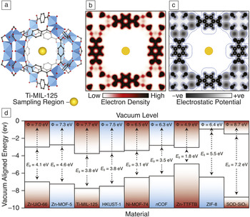
Alignment of the electronic energy levels of metal–organic frameworks (MOFs). (a) Illustration of the internal vacuum-level sampling procedure for Ti-MIL-125 along with 2D slices of the (b) electron density and (c) electrostatic potential that plateau to a constant value inside the pore, giving a well-defined reference point. (d) The calculated valence- and conduction-band positions for a range of frameworks that are discussed in the main text. Adapted with permission from Reference Reference Butler, Hendon and Walsh28. © 2014 ACS Publications. Note: E g, bandgap energy; ϕ, ionization potential; UiO, University of Oslo; MIL, Materials Institut Lavoisier; HKUST, Hong Kong University of Science and Technology; COF, covalent organic framework; ZIF, zeolitic imidazolate framework; TTFTB, tetrathiafulvalene tetrabenzoate; SOD, sodalite.

While ionization potential (electron removal energy) and electron affinity (electron addition energy) are properties that are easily defined for solids, they are difficult to quantify. It was recognized as early as the 1930s that the photoelectric threshold of solids is influenced by two factors: the bulk band energies and the surface electrostatic double layer. Reference Bardeen30 Due to the sensitivity of the surface term to the processing history, environment, and morphology of a particular sample, there is a large variation in reported values for a given compound.
Similarly, for theorists, the use of periodic boundary conditions introduces problems in predicting reliable electron energies. While periodic boundaries offer a convenient and elegant route to representing an infinite crystal from a finite repeating unit, the solution of the Coulomb interactions introduces an arbitrary reference point for the electrostatic potential, meaning that band energies cannot be compared directly between systems. Reference Walsh and Butler31–Reference Ihm, Zunger and Cohen33 In another approach, the crystal can be modeled by considering a representative cluster of finite size, which provides an external vacuum level and facilitates comparison of band energies between systems; Reference Buckeridge, Butler, Catlow, Logsdail, Scanlon, Shevlin, Woodley, Sokol and Walsh34,Reference Scanlon, Dunnill, Buckeridge, Shevlin, Logsdail, Woodley, Catlow, Powell, Palgrave, Parkin, Watson, Keal, Sherwood, Walsh and Sokol35 however, in practice, the models are challenging to construct for multicomponent systems.
In this context, we formulated a new procedure to calculate the bulk band energies of porous solids. Reference Butler, Hendon and Walsh28 The method is based on a periodic DFT approach and samples the electrostatic potential at the center of a pore where the electron density has decayed to zero and the electrostatic potential has a plateau (see Figure 2). The procedure, which is applicable to porous solids, is analogous to the use of the external vacuum level above a surface slab as a reference in solid-state calculations. The center of large pores is also a vacuum that provides a reference level for alignment between different materials.
Practically, the alignment is achieved by performing a periodic electronic structure calculation at a given level of theory. The level of theory will affect the reliability of the results, and a hybrid exchange-correlational functional (or beyond) is recommended for quantitative insights. The electrostatic (Hartree) potential at the center of the largest pore is then evaluated; this can be achieved using the MacroDensity 36 package, which we have developed for this purpose. One must ensure that the integrated value of the potential has reached a reliable convergence, which is achieved by sampling a large enough area (a sphere of radius > 2 Å) and ensuring that the variance within the sampling volume is small (< 0.01 V). The Hartree potential obtained is now referred to as the vacuum potential (V vac). The ionization potential is simply determined by subtracting the highest occupied band eigenvalue (E VB): IP = V vac – E VB. Similarly, the electron affinity is determined using the lowest unoccupied band eigenvalue (E CB). The resultant ionization potentials and electron affinities can be compared across all materials.
Access to absolute band energies allows for the design of a range of physical applications for MOFs. Recently, Cheng et al. found that using a newly designed ligand, they could obtain a material, which electronic structure calculations predict to have band energies suitable for hydrolysis and degradation of organic pollutants. Reference Wu, Wang, Zhao, Dong, Lu, Wang, Wang, Wu, Cui and Cheng37 Moreover, they experimentally demonstrated the strong photocatalytic activity of the resulting material. The alignment of energy levels has also been applied to explain the differences in photocatalytic activity in d 0 MOFs. Reference Nasalevich, Hendon, Santaclara, Svane, van der Linden, Veber, Fedin, Houtepen, van der Veen, Kapteijn, Walsh and Gascon15 Grau-Crespo and co-workers demonstrated control of frontier orbital positions by metal substitution in porphyrin-containing MOFs, allowing crystal engineering for solar-fuel production. Reference Hamad, Hernandez, Aziz, Ruiz-Salvador, Calero and Grau-Crespo38 In the context of device design, access to absolute energy levels, as well as lattice parameters from sources such as the CoRE-MOF database, will allow for the application of design strategies such as the recently developed electronic-lattice-site (ELS) metric Reference Butler, Kumagai, Oba and Walsh39 —which measures the quality of heterostructure interfaces—to fulfill the conditions of Kroemer’s lemma. These developments open the field for the design of heterojunctions featuring MOFs.
Principles for electroactivation
We now collate design principles for tailoring the physical properties. The critical criterion for realizing semiconducting MOFs is that the frontier electronic bands are delocalized (low-carrier effective masses), which requires effective communication between the organic and inorganic building blocks. However, long-range transport is not always essential, and short-range electron transfer (e.g., to an electrolyte at the surface or penetrating the pore) can be sufficient to support a wide range of redox processes.
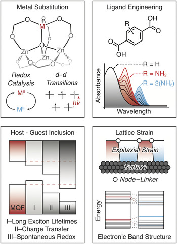
A set of four chemical principles for electroactivation of MOFs is outlined in Figure 3 . Reference Ozin40 These range from modifying the organic and inorganic building blocks that form the framework to post-synthetic modification and the application of lattice and chemical strain.
Four avenues for engineering the electronic structure and optoelectronic activity of metal–organic frameworks (MOFs) are shown. By modifying the inorganic (metal substitution) and organic (ligand engineering) units, redox processes and optical absorption can be modified. By incorporating extrinsic chemical moieties (host–guest inclusion) and mechanical effects from interfaces or embedding (lattice strain), the band offsets with respect to the valence- and conduction-band energies of the unperturbed MOF (dashed red line) can be used to control charge transport. Based on information from Reference Reference Ozin40. © 1992 Wiley. Note: h, Planck’s constant; ν, frequency; M, metal.

Metal substitution
Depending on the chemical identity and charge state, the orbitals of the metal may form the upper valence or lower conduction band of the MOF. Therefore, metal substitution has the potential to influence both oxidation (hole injection) and reduction (electron injection) processes. For example, in HKUST-1 (Hong Kong University of Science and Technology), the Cu 3d orbitals are found at the valence-band maximum, Reference Hendon and Walsh41 while in MIL-125, the Ti 3d orbitals are found at the conduction-band minimum. Beyond complete metal substitution, the formation of mixed-metal systems offers a promising route to tune redox activity. Brozek and Dincă demonstrated this for MOF-5 with Ti, V, Cr, Mn, and Fe incorporation. Reference Brozek and Dincă26
Ligand engineering
The choice of ligand can be used to tune the electronic structure directly by modifying the orbital composition or indirectly by changing the framework topology. Many MOFs have at least one frontier band centered on an organic conjugated region. The electron energies of the organic regions are therefore tunable using conventional “push-pull” principles, where the band energies are influenced by the electron-donating or withdrawing capability of additional substituents. For example, the introduction of an electron-donating primary amine to a benzene ring will result in an enhancement of electron density and a lowering of the ionization potential. Amination has been effective at introducing visible light photoactivity in a range of simple MOFs by raising the valence-band energy (e.g., modification of benzene dicarboxylate in MIL-12527 and UiO-66). Reference Nasalevich, Hendon, Santaclara, Svane, van der Linden, Veber, Fedin, Houtepen, van der Veen, Kapteijn, Walsh and Gascon15 As an alternative to ligand modification, different types of ligands are being explored (e.g., linear conjugated carboxylates have been shown to exhibit extended helical orbitals Reference Hendon, Tiana, Murray, Carbery and Walsh42 with the potential for long-range magnetic coupling). Reference Tiana, Hendon and Walsh43
Host-guest inclusion
The introduction of redox active molecular guests into a framework is one method to change the electronic properties, either through spontaneous or through light-activated charge transfer. A related process is the ability to “rewire” an insulating MOF though an auxiliary electroactive linker. The champion system in this regard is HKUST-1 modified with the molecule TCNQ (7,7,8,8-tetracyanoquinodimethane) that provided a route to tunable conductivity. Reference Talin, Centrone, Ford, Foster, Stavila, Haney, Kinney, Szalai, El Gabaly, Yoon, Léonard and Allendorf44 Allen and Cohen recently demonstrated cross-linking in a series of isoreticular MOFs, Reference Allen and Cohen22 which could be extended to install conductive pathways for a wider range of MOF topologies.
Lattice strain
A feature of porous frameworks is that they are mechanically soft and flexible in comparison to close-packed materials, which provides another route to engineer their properties. Stress and strain can be introduced in MOFs in several ways, such as by epitaxial growth on a rigid substrate, solid-state embedding of MOF particles in a host, and the application of pressure, either mechanically or chemically (e.g., defects such as missing ligands are sensitive to the growth conditions and reagents). Reference Bristow, Svane, Tiana, Skelton, Gale and Walsh45 The electronic structure response is described by the deformation potential: the change in ionization potential, electronic affinity, or bandgap with respect to a volume (pressure) change. It has been shown that the volume deformation potential is comparable to inorganic semiconductors; Reference Butler, Hendon and Walsh46 however, critically, due to smaller bulk moduli, the effects of pressure on the band gap is much larger. In the compound nCOF-1 (nCOF, noncovalent framework), the bandgap change of –2.2 eV/GPa is 20× larger than for bulk Si. Reference Hendon, Wittering, Chen, Kaveevivitchai, Popov, Butler, Wilson, Cruickshank, Miljanić and Walsh47 For these materials, a small external stimulus can result in a large change in the electronic structure.
Summary and outlook
Our discussion has focused on the successes of modern simulation techniques in describing the chemical bonding and physical properties of MOFs. While recent progress has been substantial, the a priori design of functional hybrid solids remains a daunting challenge. We have outlined fertile avenues for the pursuit of materials where the injection, extraction, excitation, and transport of charge carriers are controllable, which build on the hybrid compounds reported in the articles in this issue. Not only can the composition of the framework itself be engineered, the porosity can also be exploited for absorbate interactions that activate optical or electronic activity.
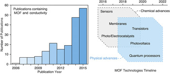
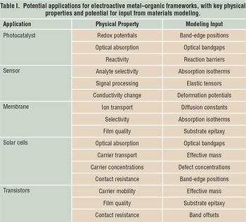
The approaches we have outlined for engineering physical properties can be exploited for the use of MOFs in a range of devices where the hybrid advantage offers the prospect of disruptive technologies. With the number of peer-reviewed papers on conductive MOFs rapidly increasing, a roadmap for future progress is illustrated in Figure 4 , 48 drawing from an earlier perspective of Allendorf et al. Reference Allendorf, Schwartzberg, Stavila and Talin49 In Table I we list several possibilities that highlight the potential role for materials modeling. Referring back to the Nobel lecture of H. Kroemer: “The principal applications of any sufficiently new and innovative technology have always been—and will continue to be—applications created by that technology.”
The increase in the number of publications on conductive metal–organic frameworks (MOFs), 48 with a projected timeline for future progress for MOF devices building on chemical and physical functionality.

Potential applications for electroactive metal–organic frameworks, with key physical properties and potential for input from materials modeling.

Acknowledgments
We thank W. Kohn and H. Kroto for the development of density functional theory and physical properties of MOF chemistry, respectively, as well as for stimulating lectures and discussions on these topics. The research discussed here has benefited from collaboration with J.K. Bristow, D. Tiana, and K.L. Svane. We acknowledge support from The Royal Society, the European Research Council (Grant No. 27757) and the EPSRC (Grant No. EP/M009580/1 and EP/K016288/1). This work used the Extreme Science and Engineering Discovery Environment (XSEDE), which is supported by the National Science Foundation Grant Number ACI-1053575.

Aron Walsh is a professor of materials design at Imperial College London. He received his BA and PhD degrees in chemistry from Trinity College, Dublin, and held positions at the National Renewable Energy Laboratory, University College London, and the University of Bath. In 2015, he was awarded the EU-40 Materials Prize from the European Materials Research Society for his work on perovskite solar cells. His research focuses on the theory and simulation of functional materials. Walsh can be reached by email at a.walsh@imperial.ac.uk.

Keith T. Butler is in the Department of Chemistry at the University of Bath. He received his BA degree in medicinal chemistry from Trinity College, Dublin and PhD degree in computational chemistry from University College London. Following postdoctoral research at the University of Sheffield on silicon solar cells, Butler joined the UK SUPERSOLAR Project at Bath to focus on next-generation materials for solar-energy conversion. Butler can be reached by phone at +44 1225384913 or by email at k.t.butler@bath.ac.uk.

Christopher H. Hendon is a postdoctoral researcher at the Massachusetts Institute of Technology. He received his BSc degree in chemistry from Monash University, Australia, and his PhD degree from the University of Bath. His research interests include the physical chemistry of metal–organic frameworks. Hendon can be reached by phone at 617-324-2161 or by email at hendon@mit.edu.