


I. INTRODUCTION
Thin films of nanocrystalline silicon (nc-Si) are considered among the most attractive materials for the third- and next-generations of solar cells and other optoelectronic devices.Reference Beard, Luther and Nozik1 Such properties of nc-Si as direct band gap (E g) optical transitions, E g dependence on the nanocrystals' size, absence of accumulation of the light-induced defects found for the case of amorphous Si (the so called Staebler–Wronski effectReference Staebler and Wronski2), and accessibility of volume processing on flexible substrates allows creating of highly efficient photovoltaic devices based on quantum dots cascade heterostructuresReference Alferov, Andreev and Rumyantsev3,Reference Yan, Yue, Xu, Yang and Guha4 and reducing processing costs due to advantages of the thin-film and roll-to-roll fabrication technologies.Reference Lewis5,Reference Søndergaard, Hösel, Angmo, Larsen-Olsen and Krebs6 Among the problems for a wide-scale commercialization of nc-Si is the lack of methods to efficiently control the size and concentration of formed Si nanocrystals. This facilitated considerable research efforts to improve existing and to develop advanced nc-Si technologies.Reference Birkholz, Selle, Conrad, Lips and Fuhs7–Reference Ro14 One of the possible approaches uses metal-induced crystallization (MIC) of amorphous Si (α-Si).Reference Nast and Wenham15–Reference van Gestel, Gordon and Poortmans17
Tin (Sn) proved to be one of the most promising metals suitable for MIC. Because Sn does not create energy levels within the crystalline Si band gap, doping of Si with Sn within the solubility levels does not affect electrical, optical, and carrier recombination properties of the crystalline Si. At the same time, doping with Sn increases resistance of Si to potentially harmful effects of the thermal treatmentReference Neimash, Kraitchinskii, Kras’ko, Puzenko, Claeys, Simoen, Svensson and Kuznetsov18 and ionizing radiation.Reference Claeys, Simoen, Neimash, Kraitchinskii, Kras’ko, Puzenko, Blondeel and Clauws19
Sn creates the eutectic alloy with SiReference Olesinski and Abbaschian20 allowing the transformation of amorphous Si into a crystalline phase through e.g., the layer exchange mechanism as was reported recently for the bi-layer structures of Sn and Si films deposited on glass substrates and annealed after the deposition.Reference Mohiddon and Krishna21,Reference Jeon, Jeong and Kamisako22 Early works on Sn-induced crystallization of α-Si showed that in the deposited from the gas phase Si–Sn mixtures, α-Si crystallization occurs when Sn concentration exceeds a certain threshold value (∼2 at.%)Reference Thornton, Elliman and Williams23 and crystal formation proceeds within the eutectic Si:Sn melt propagating ahead of the crystallization front into an α-Si region.Reference Lin and Hatalis24 Exceeding the threshold concentration of Sn entails creation of the droplets of metallic Sn, which may indicate surpassing of the solubility limit of Sn in amorphous Si, explaining also the previously reported effect of conductivity switching from the activation to hopping mechanism upon reaching exactly the same concentration of Sn in Si.Reference Parsons, Cook, Lucovsky, Lin and Mantini25,Reference Ragan, Min and Atwater26 Such coincidence of the threshold values for the three different effects (crystallization of α-Si, creation of Sn droplets, and switching of the conductivity mechanism) suggests a prime role of the metallic droplets of Sn in initiating crystallization in the α-Si:Sn system. This idea agrees well with the experimental data on α-Si crystallization upon thermal anneal of the planar bi-layered Si–Sn structures.Reference Mohiddon and Krishna21
Recent studies on Sn-induced crystallization of α-Si demonstrated transformation of up to 90% of α-Si volume into a nanocrystalline phase with crystal sizes of 2–5 nm.Reference Voitovych, Neimash, Krasko, Kolosiuk, Povarchuk, Rudenko, Makara, Petrunya, Juhimchuk and Strelchuk27–Reference Neimash, Poroshin, Shepeliavyi, Yukhymchuk, Melnyk, Kuzmich, Makara and Goushcha29 The experimental results were treated using an approach that was essentially different from the conventional MIC mechanisms. In particular, Si crystallization was shown to occur within molten eutectic regions around the droplets of liquid Sn, and the size of formed nanocrystals decreased with distance from the droplets, evidencing that crystallization is limited by the width of the molten eutectic region, controlled by Sn supply to the Si:Sn alloy. These observations allowed proposing the crystallization mechanism that involves self-sustained, cyclic transitions between the super-saturated and under-saturated states of the Si:Sn eutectic formed at the interface with microscopic droplets of molten Sn. The current work focuses on verification of the suggested in Ref. Reference Neimash, Poroshin, Shepeliavyi, Yukhymchuk, Melnyk, Kuzmich, Makara and Goushcha29 mechanism by applying experimental and theoretical modeling.
II. SAMPLES AND EXPERIMENTAL METHODS
We studied engineered macroscopic-size films of Sn embedded in α-Si matrix. The planar structures shown schematically in Fig. 1 were fabricated using thermal evaporation of electronic-grade (99.99%) Si and Sn (99.92%). The structures were formed in three steps. First, an amorphous Si layer (X in Fig. 1) of 100 nm thickness was deposited on a borosilicate glass substrate (BSG in Fig. 1) at 150 °С. During the second step, a 100 nm thickness layer of metallic Sn (Y in Fig. 1) was formed in the same vacuum chamber using deposition through the mask. The second layer of amorphous Si (Z in Fig. 1) of 100 nm thickness was deposited during the third processing step. Each of the three deposition steps was performed during a single load in a vacuum chamber at a residual pressure of 10−3 Pa by a sequential use of the three different evaporators. The structures created using the method described above can be considered as an analog of Sn microdroplets seeded inside the amorphous Si matrix. The samples were annealed for 30 min at 300 and 400 °С and the effects of anneal on the film micro structure as well as distribution of the formed components were studied.
Schematic representation of a planar structure used to study the crystallization mechanism of α-Si/Sn alloys. BSG is a substrate; X—first deposited layer of α-Si; Y—metallic Sn; Z—second deposited layer of α-Si. The thickness of the deposited layers was X = Y = Z = 100 nm. A and B indicate the locations of laser beam incidence for Raman spectra measurements.

The amorphous versus crystalline phase composition of the films was analyzed using room temperature Raman spectroscopy (RS, JobinYvon Т-64000) activated with Ar+-laser at the wave length of 514.5 nm. The laser spot diameter varied from 3 to 300 μm. The impurity distribution profiles across the structures were characterized with the Auger electron spectroscopy (Riber Las 2000) during ion etching (RIE) of films using 3 keV energy Ar+ ions with the etch rate of 12–14 nm/min. A typical surface area exposed to the ion beam was a ∼1 mm diameter spot. The surface topology and structure were studied by scanning electron microscopy (SEM, JSM-840, Peabody, MA).
III. EXPERIMENTAL RESULTS
Figure 2 shows Raman spectra of the engineered structure Si/Sn/Si, recorded right after deposition (spectra 1 and 2) and following 30 min of anneal in vacuum at 300 °С (spectra 3 and 4) and 400 °С (spectrum 5). Spectra 1 and 4 were recorded from the region outside the deposited Sn layer, which is shown schematically as locations B in Fig. 1. Spectra 2, 3, and 5 were measured in the locations A (see Fig. 1) within the central portion of the film, above the deposited Sn layer. The characteristic feature of the spectra 1 and 4 is a broad band with a maximum centered around 470 cm−1, typical for the amorphous Si.Reference Richter, Wang and Ley30 No signature of crystalline Si (c-Si) was revealed in the spectra 1 and 4. In contrast, spectra 2, 3, and 5 contained signatures of a Si crystalline phase—the additional sharp peaks at 505, 512, and 515 cm−1, respectively.Reference Richter, Wang and Ley30–Reference Bustarret, Hachicha and Brunel32 Evidently, the crystalline phase in the center portion of the sample was formed during the deposition of the film (see spectrum 2). Applying analysis described in Ref. Reference Neimash, Poroshin, Shepeliavyi, Yukhymchuk, Melnyk, Kuzmich, Makara and Goushcha29, the average size of the crystals increased from 2.7 nm right after the film deposition to 3.2 nm after thermal annealing at 300 °С and to 4.5 nm after further annealing at 400 °С. At the same time, the partial volume of the crystalline phase increased more than twofold.
The concentration distribution of chemical elements across the center portion of the as-grown Si/Sn/Si structure studied with the Auger spectroscopy is shown in Fig. 3(a). The left-hand side of the distribution corresponds to the top surface of a sample; the right-hand side corresponds to the BSG substrate. A relatively high concentration of technological impurities oxygen and carbon was due to a rather low vacuum level in the deposition chamber.
(a) Concentration profiles of the as-grown Si/Sn/Si structure taken from the center portion of the sample (location A in Fig. 1) using the etch rate of 12–14 nm/min; (b) SEM image of the center portion of the sample.
The top surface of the deposited Si/Sn/Si stack reveals microscopic-size spheres with the diameter ranging from 120 to 470 nm [Fig. 3(b)]. Obviously, Fig. 3(a) reflects distributions averaged across multiple spheres imaged in Fig. 3(b) (the ion beam diameter in Auger measurements was ∼1 mm). The depth of a broad maximum of Sn concentration at ∼45 at.% in Fig. 3(a) corresponds to the spheres' average radius, whereas two maximums of Si concentration (one at ∼60 at.%, close to the top surface and the other at ∼90 at.%, close to the substrate) correspond to the predominant locations of Si around the periphery of an average sphere. This suggests a metallic Sn core covered with Si shell for a composition of each sphere. Most probably, metallic cores in the form of molten droplets of Sn were formed during the deposition of Sn on the first layer of α-Si due to heating of this layer to above 229 °C caused by the flux of atomic Sn and radiation from the evaporator. When depositing the second layer of α-Si, the metallic cores were covered with α-Si shells that partially crystallized while Sn cores remained molten. The spheres exhibit venation patterns at the surface, which resembles the ornament on the surface of microscopic metallic Sn droplets formed within the alloyed Si:Sn films studied in Ref. Reference Neimash, Poroshin, Shepeliavyi, Yukhymchuk, Melnyk, Kuzmich, Makara and Goushcha29. These patterns are most probably the cracks created in the Si shell due to mismatch in the temperature expansion coefficients of the Sn core and Si shell.
Thermal anneal of the as-grown samples changes their structure. Sn distribution across the sample after 30 min of annealing at 300 °C became nearly uniform [Fig. 4(a)]. Si also appeared to be distributed considerably more uniformly after anneal. Evidently, upon thermal anneal the components (Si and Sn) mixed up, facilitating formation of the crystalline phase of Si (recall a two-fold increase in the portion of the crystalline phase after anneal as evidenced by Fig. 2). Since the Si:Sn eutectic point temperature is low (231.9 °C),Reference Olesinski and Abbaschian20 this mixing proves that crystallization occurs due to eutectic formation, supporting the mechanism proposed in Ref. Reference Neimash, Poroshin, Shepeliavyi, Yukhymchuk, Melnyk, Kuzmich, Makara and Goushcha29. An increase in oxygen content was due to additional exposure to an ambient atmosphere. As is known, oxygen in the observed concentrations does not affect crystallization.Reference Neimash, Poroshin, Kabaldin, Yukhymchuk, Shepelyavyi, Makara and Larkin28,Reference Neimash, Poroshin, Shepeliavyi, Yukhymchuk, Melnyk, Kuzmich, Makara and Goushcha29 A venation pattern at the surface of the spheres was replaced with the light convexities (c-Si phase) and the bright spherical features appeared in-between the spheres [Fig. 3(b)]. Energy dispersive x-ray spectroscopy studies proved that these bright spherical features are the droplets of the metallic Sn (not shown on the figure), suggesting that during crystallization the excessive Sn atoms leave silicon shell and collect into metallic droplets, revealing bright spherical features in SEM images.
(a) Concentration profiles in a center portion of the Si/Sn/Si sample (location A in Fig. 1) after anneal at 300 °C; (b) SEM-image of the same sample.
Experimental results presented above evidenced that the macroscopic-size film of metallic Sn sandwiched between α-Si layers (exemplified by the schematic representation of Fig. 1) disintegrated into multiple nanometer-size droplets during the deposition of the metallic film and top α-Si layer. The top α-Si layer covered liquid Sn droplets thus forming their shells and producing the elements distribution in Auger analysis concurring with Fig. 3(a). A distinct peak at 505 cm−1 in the Raman spectrum of Fig. 2 (curve 2) proves that a partial crystallization of Si occurred during the sample growth. Crystallization of Si continued upon further thermal anneal of the samples when Sn droplets melted again (spectra 3 and 5 in Fig. 2), facilitating an ultimate quasi-uniform distribution of Sn across the thickness of the whole structure as was detected by the Auger analysis [Fig. 4(a)]. All experimentally observed features of the formed crystalline phase, like nanocrystals formation around Sn droplets, dominant sizes of nanocrystals and their dependence upon anneal conditions, squeezing the excess Sn off the crystalline phase, etc. were similar to those reported recently for the case of crystallization around the isolated microscopic droplets of molten Sn embedded in α-Si matrix.Reference Neimash, Poroshin, Shepeliavyi, Yukhymchuk, Melnyk, Kuzmich, Makara and Goushcha29 In accordance with the mechanism suggested in Ref. Reference Neimash, Poroshin, Shepeliavyi, Yukhymchuk, Melnyk, Kuzmich, Makara and Goushcha29, Si crystallization may be considered as a process occurring cyclically within the molten regions of liquid Sn saturated with Si.
IV. THEORETICAL MODEL
Consider a simple kinetic model that allows analyzing a cyclic propagation of the crystallization front in the system α-Si/eutectic Si:Sn/c-Si. Consider a one-dimensional case and assume that at the instant t = 0 the Si:Sn eutectic occupies the space 0 ≤ x ≤ x 0, the crystalline phase fills the half-space x < 0, and the α-Si matrix extends over x > x 0. Let us assume that there is no replenishment of Sn from outside of the eutectic and the excessive Sn atoms are squeezed out of the region 0 ≤ x ≤ x 0. In contrast, Si can be supplied to the eutectic from the region x > x 0.
Let us further assume no chemical reactions in the system and a complete diffusion control of the system's composition and dynamics. Let the Si diffusion constant D Si be independent of the volume fraction  $\phi$ of the crystalline phase formed within the eutectic region. Assume also that D Si is the same for α-Si and eutectic regions. Consider a constant bath temperature outside of the eutectic. For this simplified case, the evolution of heat and volume concentration (N Si) of Si atoms in the eutectic region can be written using the following governing equations:
 $${{\partial T} \over {\partial t}} = \kappa {{{\partial ^2}T} \over {\partial {x^2}}} + {{{H_{\rm{c}}}} \over {\rho C}}{{\partial \phi } \over {\partial t}} - {{{H_{\rm{a}}}} \over {\rho C}}{{\partial {N_{\rm{a}}}} \over {\partial t}}\delta \left( {x - {x_0}} \right)\quad ,$$
 $${{\partial {N_{{\rm{Si}}}}} \over {\partial t}} = {D_{{\rm{Si}}}}{{{\partial ^2}{N_{{\rm{Si}}}}} \over {\partial {x^2}}} - {1 \over {\left( {1 - \phi } \right)}}\left( {{N_{{\rm{Sn}}}}{{\partial \phi } \over {\partial t}}} \right) + {{\partial {N_{\rm{a}}}} \over {\partial t}}\delta \left( {x - {x_0}} \right)\quad .$$
Equation (1) describes changes of the absolute temperature T due to (i) thermal transfer with the thermal diffusivity κ, (ii) latent heat H c release during crystallization, and (iii) latent heat H a consumption during the dissolution of amorphous Si. ρ and C are the solid phase (both crystalline and amorphous) volumetric mass density and specific heat capacity, respectively. The Dirac delta factor δ(x − x 0) accounts for the fact that heat consumption due to α-Si dissolution and related changes in the volume concentration N a of α-Si occur at the eutectic region boundary.
Equation (2) describes the changes in Si atoms volume concentration within the eutectic region due to mass diffusion (the first term) and crystallization (the second term). The expression  $\left( {{N_{{\rm{Sn}}}}{{\partial \phi } \over {\partial t}}} \right)$ accounts for Si consumption caused by crystallization and the factor
 ${1 \mathord{\left/ {\vphantom {1 {\left( {1 - \phi } \right)}}} \right. \kern-\nulldelimiterspace} {\left( {1 - \phi } \right)}}$ is the correction for the partial volume change on the concentration change.Reference Hort and Spohn33 The third term in the right-hand side of Eq. (2) accounts for a steady supply of Si atoms from the amorphous phase at the eutectic region boundary. The time evolution of the Sn volume concentration N Sn may be formalized similarly to Eq. (2); however, such formalization will not be used in this work since our analysis is focused on evolution of the crystalline Si phase.
To allow solution of governing Eqs. (1) and (2), the mechanism of crystals formation has to be chosen and the function  ${{\partial \phi } \mathord{\left/ {\vphantom {{\partial \phi } {\partial t}}} \right. \kern-\nulldelimiterspace} {\partial t}}$ defined. Assuming crystallization by nucleation processReference Becker and Döring34 and using a simple phenomenological approach, the steady-state rate J of nuclei formation per unit volume can be modeled asReference Tavare35:
 $$J\left( T \right) = {k_{\rm{n}}}{\left[ {{N_{{\rm{Si}}}} - N_{Si}^{\rm{e}}\left( T \right)} \right]^m}\quad ,$$
where k n is the temperature-independent rate constant,  $N_{{\rm{Si}}}^{\rm{e}}\left( T \right)$ the temperature-dependent Si monomers' equilibrium concentration at saturation, and m an empirical exponent. The difference
 $\left[ {{N_{{\rm{Si}}}} - N_{{\rm{Si}}}^{\rm{e}}\left( T \right)} \right]$ describes the alloy super-saturation. The values of k n and m are considered as tuning parameters for numeric modeling of the results. Assuming that the crystalline phase consists of nuclei of the critical size only (no crystal growth is allowed), the master equation that describes evolution of the volume fraction
 $\phi$ of the crystalline phase reads:
 $${{\partial \phi } \over {\partial t}} = {\upsilon _{\rm{c}}}J\left( T \right)\quad ,$$
in which υc = 4/3πvR c3 is the fractional volume of a critical nucleus with the radius R c and v the dimension scaling factor. Combining Eqs. (3) and (4) yields the final version of the master equation for  $\phi$:
 $${{\partial \phi } \over {\partial t}} = {4 \over 3}\pi vR_{\rm{c}}^3{k_{\rm{n}}}{\left[ {{N_{{\rm{Si}}}} - N_{{\rm{Si}}}^{\rm{e}}\left( T \right)} \right]^m}\quad .$$
Alternatively,  $\phi \left( t \right)$ may be defined using a classical nucleation theory for R c and J(T) like it was made recently to describe aluminum-induce α-Si crystallizationReference Sarikov, Schneider, Muske, Gall and Fuhs36 Among the other alternatives is using the Johnson–Mehl–Avrami–Kolmogorov (JMAK) equation for the rate of the crystalline phase growthReference Avrami37 or advanced crystallization theories described elsewhere.Reference Clouet, Furrer and Semiatin38 However, the JMAK equation as well as the classical nucleation theory and other advanced theories include growth of the formed nuclei, which adds complexity to our consideration not changing the results qualitatively.
Let us consider a stationary-state solution  ${{\partial T} \mathord{\left/ {\vphantom {{\partial T} {\partial t}}} \right. \kern-\nulldelimiterspace} {\partial t}} = 0$, imposing no temperature change within the eutectic region. Equalizing to zero the right-hand side of Eq. (1) and integrating it over x from x = 0 to x = x 0, obtain:
 $$\kappa {\left. {{{\partial T} \over {\partial x}}} \right|_{x = {x_0}}} - \kappa {\left. {{{\partial T} \over {\partial x}}} \right|_{x = 0}} = - {x_0}{{{H_{\rm{c}}}} \over {\rho C}}{{\partial \phi } \over {\partial t}} + {1 \over 2}{{{H_a}} \over {\rho C}}{{\partial {N_{\rm{a}}}} \over {\partial t}}\quad ,$$
which represents the energy balance of the system. The left hand side of Eq. (6), 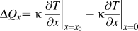 $\Delta {Q_x} \equiv \;\kappa\; {\left. {{{\partial T} \over {\partial x}}} \right|_{x = {x_0}}} - \kappa {\left. {{{\partial T} \over {\partial x}}} \right|_{x = 0}}$, describes the heat transfer from or into the eutectic region under the conditions of unchanged temperature:
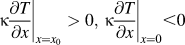
(i) If ΔQ x < 0, the heat is transferred from the bath to within the eutectic region (0; x 0), valid when the temperature at the boundaries inside the region (0; x 0) is lower than outside it:
 $\kappa {\left. {{{\partial T} \over {\partial x}}} \right|_{x = {x_0}}} > 0,\,\kappa {\left. {{{\partial T} \over {\partial x}}} \right|_{x = 0}} \lt 0$.
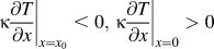
(ii) If ΔQ x > 0, the heat is transferred from the eutectic region (0; x 0) to the bath, valid when the temperature at the boundaries inside the region (0; x 0) is higher than outside it:
$\kappa {\left. {{{\partial T} \over {\partial x}}} \right|_{x = {x_0}}} \;\lt\; 0,\,\kappa {\left. {{{\partial T} \over {\partial x}}} \right|_{x = 0}} > 0$.
The occurrence of either of the two cases above depends on the sign of the expression  ${A_x} \;\equiv\; - {x_0}{{{H_{\rm{c}}}} \over {\rho C}}{{\partial \phi } \over {\partial t}} + {1 \over 2}{{{H_{\rm{a}}}} \over {\rho C}}{{\partial {N_{\rm{a}}}} \over {\partial t}}$.
The condition A x = 0 defines a critical point, at which the eutectic region is triggered between the two states—either consumption of heat from the surrounding bath or release of excessive heat to the outside regions. The sign of A x is controlled by the magnitude of  ${{\partial \phi } \mathord{\left/ {\vphantom {{\partial \phi } {\partial t}}} \right. \kern-\nulldelimiterspace} {\partial t}}$ defined by the master Eq. (5). If, for example, at a given instant the rate of nuclei formation increases, causing
 ${{\partial \phi } \mathord{\left/ {\vphantom {{\partial \phi } {\partial t}}} \right. \kern-\nulldelimiterspace} {\partial t}} > 0$, then A x becomes negative and the eutectic starts consuming heat from the surrounding regions. Such heat consumption breaks eventually the stationary-state condition
 ${{\partial T} \mathord{\left/ {\vphantom {{\partial T} {\partial t}}} \right. \kern-\nulldelimiterspace} {\partial t}} = 0$, and the temperature starts raising, pushing the eutectic below the saturation level. This causes decrease in the rate of nuclei formation, slowing the crystallization and switching the rate of the volume fraction
 $\phi$ change to
 ${{\partial \phi } \mathord{\left/ {\vphantom {{\partial \phi } {\partial t}}} \right. \kern-\nulldelimiterspace} {\partial t}} \;\lt \;0$. The rise in the eutectic temperature slows down, facilitating attaining the stationary-state condition
 ${{\partial T} \mathord{\left/ {\vphantom {{\partial T} {\partial t}}} \right. \kern-\nulldelimiterspace} {\partial t}} = 0$.
Further decrease of  ${{\partial \phi } \mathord{\left/ {\vphantom {{\partial \phi } {\partial t}}} \right. \kern-\nulldelimiterspace} {\partial t}}$ causes the A x increase. When A x becomes positive, the eutectic starts releasing the heat to outside regions, which eventually breaks the stationary-state condition
 ${{\partial T} \mathord{\left/ {\vphantom {{\partial T} {\partial t}}} \right. \kern-\nulldelimiterspace} {\partial t}} = 0$, at which point the temperature starts decreasing, pushing the eutectic into a super-saturation mode with
 ${{\partial \phi } \mathord{\left/ {\vphantom {{\partial \phi } {\partial t}}} \right. \kern-\nulldelimiterspace} {\partial t}} > 0$. Such periodic changes of the crystalline phase formation rate and related changes in the eutectic temperature will persist until
 $\phi$ → 1 (which also means a complete exhaust of Sn supply). Alternatively, a cyclic crystallization may stop upon consumption of all α-Si and squeezing of Sn outside a newly formed phase.
V. DISCUSSION
Experimental results of this work support the mechanism of α-Si crystallization proposed recently,Reference Neimash, Poroshin, Shepeliavyi, Yukhymchuk, Melnyk, Kuzmich, Makara and Goushcha29 in which the nucleation of nc-Si occurs within the droplets of liquid Sn saturated with atoms of Si (eutectic solution of Si in Sn). Due to electron screening effectReference Hiraki39 and diffusion, atoms of Si and Sn cross the Si/Sn interface and mix partially with each other, creating molten eutectic Si:Sn regions composed of Si dissolved in Sn. Dissolution of α-Si proceeds with absorption of heat, causing a gradual decrease in temperature upon saturating the eutectic regions with Si. When the Si:Sn melt becomes super-saturated, crystallization of Si begins either through the spinodal decomposition or nucleation process. The number of created nanocrystals increases with time and they become larger that can be detected with RS (Fig. 2, spectra 2,3,5). Concurrently, Si crystallization initiates two processes tending to revert the alloy into an under-saturated state. First process is Sn segregation on the surface of growing Si crystals. Since the solubility of Sn in crystalline Si is very low (∼5 × 1019 cm−3),Reference Olesinski and Abbaschian20 the excess Sn atoms are squeezed out of the formed nanocrystals, thereby lowering the saturation level of the surrounding eutectic regions. The second process is crystallization (latent) heat release upon formation and growth of nanocrystals, which causes a local temperature increase and, consequently pushes the system below the saturation level. These two processes trigger restoring of α-Si dissolution within the eutectic regions, which in turn forces the eutectic toward super-saturation. Repeated cyclically, the two processes that push the eutectic into the under-saturation mode, on the one hand, and the process that facilitates super-saturation of the eutectic, on the other hand, cause a cyclic formation of nanocrystals and expansion of the crystalline phase into the α-Si matrix that surrounds Sn droplets.
Accumulation of crystalline phase with time during the amorphous phase dissolution is predetermined by a significantly lower solubility of the crystalline Si in Sn compared to the solubility of α-Si in Sn. Apparently, prevailing dissolution of α-Si is facilitated by multiple dangling bonds in α-Si and absence of the crystallographic symmetry, which leads to a significant reduction of the interatomic binding energy in amorphous Si compared to that in the crystalline Si. Sn–Si phase diagram shows that the eutectic point (the lowest temperature of co-existence of Si and Sn in liquid phases, 231.9 °C) approaches closely the melting point of Sn.Reference Olesinski and Abbaschian20 Close to the eutectic point, a solubility of Si in Sn decreases to very small values. At the temperatures of 300–400 °C, even a tiny amount of α-Si dissolved in Sn could create super-saturation and trigger crystallization. On the other hand, any small drop in Si concentration, caused by crystallization within the eutectic layer, leads to a considerable increase of the local temperature and, hence, resumes dissolution of α-Si ceasing therefore crystallization. As was discussed above, each of the two processes—Si crystallization and dissolution—leads to temperature change within the eutectic regions in the direction opposite to the one that triggered these processes, thereby providing the necessary feedback that pushes the system back to equilibrium and supports a cyclic character of α-Si dissolving in Sn and formation of Si nanocrystals within the eutectic regions. The role of metallic Sn is to constantly supply Sn to the eutectic through mass diffusion to support α-Si dissolution. However, as crystallization progresses, the eutectic layer moves further away from the metallic Sn and becomes thinner, causing a gradual exhaust of Sn supply.
Similar effects of low temperature, Sn-induced crystallization of germanium (Ge) within the eutectic layer were reported recently suggesting higher than the equilibrium solid solubility of Sn in Ge.Reference Chikita, Matsumura, Kai, Sadoh and Miyao40,Reference Toko, Oya, Saitoh, Yoshizawa and Suemasu41 For the case of MIC of Si, the estimations of Sn content in a solid phase of Sn1−x Six could also be done by analyzing spectral distributions of the vibrational modes Sn–Sn, Sn–Si, and Si–Si. However, an accurate analysis could be made only under conditions of a complete transformation of the amorphous Si into a nanocrystalline phase. If a portion of the amorphous phase (α-Si) still remains not crystallized, the low-intensity vibrational modes Sn–Sn and Sn–Si overlap with the dominant TO-, LA-, LO, and TA-bands of α-Si. In addition, Raman band of the nanocrystalline phase also contributes within the same frequency range. The spectral position of this band depends on the average size of nanocrystals and some other factors (stress and components composition), making an accurate quantitative analysis even more difficult if not impossible.
Sn-induced crystallization of α-Si proved to proceed with very high efficiency. A transformation of up to 90% of the amorphous phase into nanocrystalline Si was reported in our previous works.Reference Voitovych, Neimash, Krasko, Kolosiuk, Povarchuk, Rudenko, Makara, Petrunya, Juhimchuk and Strelchuk27–Reference Neimash, Poroshin, Shepeliavyi, Yukhymchuk, Melnyk, Kuzmich, Makara and Goushcha29 Even higher conversion rates (up to 99%) were reported for aluminum-induced crystallization of Si,Reference Toko, Numata, Saitoh, Yoshizawa, Usami and Suemasu42,Reference Numata, Toko, Saitoh, Yoshizawa, Usami and Suemasu43 although the mechanism of Al-induced crystallization is known to be different from the mechanism discussed here. A complete crystallization in the Sn:Si mixture could be achieved at higher temperatures and longer anneal time. The possibility and conditions of such conversion will be explored in our further works.
The engineered quasi-2D structures (Fig. 1) studied in this work resemble the layered Sn–Si structures, in which Si crystallization via the layer exchange mechanism was reported.Reference Mohiddon, Krishna and Marcello16 However, despite a partial similarity of the engineered structures, we did not observe Si crystallization through an exchange of Si and Sn layers. Most probably, a few distinct differences in the stack formation and deposition conditions facilitated the formation of Sn droplets surrounded with the eutectic shell, creating thereby conditions for Si crystallization within those shells in our experiments. In fact, the crystallization occurs inside these eutectic shells due to consumption of material from the neighboring α-Si regions and Sn droplets. At the same time, saturation of Sn droplets with Si atoms through consumption of α-Si and squeezing of metallic Sn out of formed Si nanocrystals could be considered as a kind of exchange events, resembling thereby the features of crystallization via the layer exchange mechanism.
The theoretical model [Eqs. (1), (2), and (5)] used to describe the crystallization phase propagation belongs to the formalism of nonlinear dynamics,Reference Nicolis and Prigogine44,Reference Haken45 widely used to describe instabilities of the eutectic temperature and phase composition upon crystals formation and the crystallization front propagation.Reference Toramaru46–Reference Kurtze, van Saarloos and Weeks49 The instability modes usually reveal oscillating solutions, indicating that under certain conditions, controlled by various parameters including the rate of components supply to the eutectic via diffusion, the crystallization front propagates cyclically within the eutectic region and the partial volume of the crystalline phase may exhibit oscillating behaviors.Reference Toramaru and Matsumoto47,Reference Kurtze, van Saarloos and Weeks49–Reference Smagin and Nepomnyashchy51 The presented model takes into account main features suggested from the experimental observations, showing qualitatively that the partial volume of the crystalline phase may reveal a cyclic growth/decay until either Sn supply or α-Si is completely exhausted. The other variables of the system, such as the eutectic temperature and the rate of critical nuclei formation may also exhibit oscillatory behaviors. The driving force for such cyclic (oscillating) behavior is the difference in internal energies of the amorphous and crystalline Si phases as well as the Gibbs free energy difference of Si in the all Si matrix and Si:Sn molten alloy. The ultimate result of such oscillations is a complete transformation of α-Si into a crystalline state. To determine specific conditions and parameters' domains for self-sustained oscillating behavior of the system, separate studies featuring numerical solution of Eqs. (1), (2), and (5) are required.
A molten alloy of Si with Sn is used for purification of metallurgical Si during its re-crystallization.Reference Wakefield and Setty52,Reference Maronchuk, Kulyutkina and Maronchuk53 This is usually achieved at high temperatures to provide high solubility of Si in Sn and allow formation of crystals with dominant size much larger than that of the nanocrystals in our studies. As an example, in a recent study, the metallurgical Si was dissolved in molten Sn at 1200 °C, at which temperature the Si solubility is ∼15 at.%.Reference Maronchuk, Kulyutkina and Maronchuk53 Then the temperature was decreased to 700 °C to create super-saturation of the solution with Si that triggered crystallization (Si solubility in Sn at 700 °C is ∼1 at.%). The sizes of crystallites formed using this method were within the range of 100–200 µm. For low-temperature conditions (300–500 °С), the dominant size of the crystallites is much smaller, typically within the range of several nanometers.Reference Mohiddon, Krishna and Marcello16 The nanocrystals having a dominant size of 2–5 nm were observed recently within the eutectic layer surrounding micro droplets of Sn at 300 °С.Reference Neimash, Poroshin, Shepeliavyi, Yukhymchuk, Melnyk, Kuzmich, Makara and Goushcha29 The nanocrystals of the same size were formed in the current study using the engineered quazi-2D droplet of Sn to mimic crystallization process reported in Ref. Reference Neimash, Poroshin, Shepeliavyi, Yukhymchuk, Melnyk, Kuzmich, Makara and Goushcha29.
Note an important advantage of Si crystallization using the gas-phase deposition of α-Si on molten Sn over high-temperature dissolving of amorphous Si in Sn. During the gas-phase deposition, the eutectic layer formation does not require breaking Si interatomic bonds, thereby favoring nearly instantaneous creation of nanocrystals within the eutectic layer at relatively low temperatures. This conclusion correlates with the high rate of Si nanocrystals formation in the deposited films of Si:Sn alloysReference Voitovych, Neimash, Krasko, Kolosiuk, Povarchuk, Rudenko, Makara, Petrunya, Juhimchuk and Strelchuk27–Reference Neimash, Poroshin, Shepeliavyi, Yukhymchuk, Melnyk, Kuzmich, Makara and Goushcha29 and explains highly efficient growth of nanocrystals during the second Si layer deposition on top of Sn layer observed in the present study.
Smooth dependence of the nanocrystals size and concentration on the temperature and anneal time demonstrated in this work allows development of new nc-Si technologies based on the discussed mechanism. The low temperature of nanometer-size crystals formation, high rate of films deposition, as well as simplicity of the applied processing methods may facilitate utilization of not expensive polymer-based substrates and roll-to-roll technologies in solar cells fabrication. Our experimental results demonstrated the formation of nc-Si phase with ∼10% of the metallic Sn content. Removal of this residual Sn from the regions between nanocrystals could be achieved using known in the industry methods, tuned for volume production. At the same time, small amounts of Sn dissolved in nc-Si should not create problems related to charge trapping or other unwanted processes since Sn as a dopant does not create energy levels in the Si band gap.
VI. CONCLUSIONS
Results reported in this work support the model describing the mechanisms of Sn-induced α-Si crystallization proposed in our recent work.Reference Neimash, Poroshin, Shepeliavyi, Yukhymchuk, Melnyk, Kuzmich, Makara and Goushcha29 Among the important features of the model are (i) formation of microscopic droplets of metallic Sn within the α-Si matrix; (ii) dissolving of Si in molten Sn at temperatures higher than the Sn melting temperature followed by formation of Si:Sn eutectic layers, in which Si crystallization occurs facilitated by an efficient exchange (diffusion) of Si and Sn atoms with the adjacent α-Si matrix and molten Sn droplets; (iii) cyclic character of both Si atoms supply to the Si:Sn eutectic and Si atoms exit from the eutectic to precipitations, resulting in complete dissolution of α-Si and formation of nc-Si. Obviously, the features (ii) and (iii) are the common characteristics of the mechanism of Sn-induced transformation of Si from its amorphous state into crystalline state. Such transformation does not depend on the shape and scale of the interfacial layer between α-Si and metallic Sn—whether it is the macroscopic bi-layer Si/Sn structure,Reference Mohiddon and Krishna21,Reference Jeon, Jeong and Kamisako22 microscopic Sn droplets within a Si film,Reference Neimash, Poroshin, Shepeliavyi, Yukhymchuk, Melnyk, Kuzmich, Makara and Goushcha29 or Si spheres with Sn cores like those discussed in this work. The same mechanism, with some modifications, can be successfully applied to describe metal-induced Si crystallization by other eutectic-forming metals.



