I. INTRODUCTION
Flexible, stretchable pressure sensors with high sensitivity show promise in applications including touch screens, biomedical diagnostic technologies such as wearable heart rate monitors, and artificial “electronic skin” for robots or prosthetic devices. Reference Zhao, Hua, Yu, Zhang and Pan1–Reference Wagner, Lacour, Jones, Hsu, Sturm, Li and Suo8 To mimic the full range of human skin pressure sensitivity, there exists a need for low-cost and scalable methods for producing pressure-sensing pixels that sense both medium-pressures (10–100 kPa) and low-pressures (<10 kPa). Reference Pan, Chortos, Yu, Wang, Issacson, Allen, Shi, Dauskardt and Bao9,Reference Sergio, Manaresi, Campi, Canegallo, Tartagni and Guerrieri10
Capacitive pressure sensors have demonstrated high accuracy in detecting static loads, reproducible performance over many cycles of use, and robust function under a variety of conditions. Reference Sergio, Manaresi, Campi, Canegallo, Tartagni and Guerrieri10–Reference Lipomi, Vosgueritchian, Tee, Hellstrom, Lee, Fox and Bao12 The dielectric layer controls the capacitance (C) of the device by the relation
 $$C = {\varepsilon _{\rm{r}}}{\varepsilon _0}{A \over d}\quad ,$$
where εr is the dielectric constant, ε0 is the permittivity of free space, A is the surface area of the parallel plates, and d is the distance between them. Thus, a capacitive pressure sensor can respond to applied mechanical force via a change in capacitance due to (i) a change in the dielectric constant of the material between the electrodes (εr), or (ii) a change in the distance between the electrodes (d).
Capacitive sensors therefore require a dielectric material that is easily compressed and responds quickly to application and release of pressure. In addition to the use of foams as dielectric materials for sensing moderate-pressures, Reference Metzger, Gleisch, Meyer, Dansachmüller, Graz, Kaltenbrunner, Keplinger, Schwödiauer and Bauer11 elastomers have been incorporated into capacitive pressure sensors. In particular, polydimethylsiloxane (PDMS) shows promise as a flexible, biocompatible material for dielectric films. Reference Hammock, Chortos, Tee, Tok and Bao6,Reference Ramuz, Tee, Tok and Bao7,Reference Lipomi, Vosgueritchian, Tee, Hellstrom, Lee, Fox and Bao12–Reference Woo, Kong, Kim and Kim17 However, unstructured PDMS thin films possess high viscoelasticity, which prevents rapid response and relaxation and leads to poor sensitivity. As a result, our group pursued a strategy of microstructuring the PDMS to introduce air into the dielectric layer and enable elastic deformation of the material. Dielectrics with microstructured lines or pyramid patterns were fabricated using silicon molds that had been photolithographically patterned and etched in potassium hydroxide. Reference Mannsfeld, Tee, Stoltenberg, Chen, Barman, Muir, Sokolov, Reese and Bao13 However, the pressure sensors produced exhibited high sensitivities (up to 0.55 kPa−1) only within the narrow range of 0–7 kPa. Reference Mannsfeld, Tee, Stoltenberg, Chen, Barman, Muir, Sokolov, Reese and Bao13,Reference Tee, Chortos, Dunn, Schwartz, Eason and Bao15 We subsequently found that the sizes of and spacing between pyramids could be adjusted, but the methods used possessed similar limitations. Reference Tee, Chortos, Dunn, Schwartz, Eason and Bao15 For the large-scale fabrication of such sensors, it is desirable to have a simple, low-cost, tunable method for producing microstructured compressible layers with the desired sensitivity over a wide range of pressures.
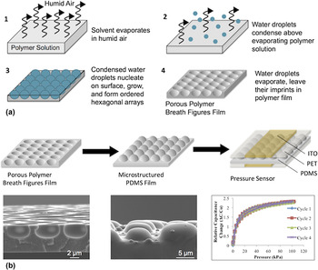
The breath figures (BFs) patterning technique represents a simple, robust method for producing microstructured honeycomb-patterned porous polymer films. Reference Hernández-Guerrero and Stenzel18,Reference Bunz19 “Breath figures,” discovered as early as 1892, refer to the organized arrays of water droplets that form when humid air comes in contact with cold solid or liquid surfaces. Reference Hernández-Guerrero and Stenzel18,Reference Croft20,Reference Sun, Shao and Ji21 In the BFs method [Fig. 1(a)], water droplets from a flow of humid air condense above the surface of a polymer solution, cooled by the evaporating solvent. This results in a highly ordered, monodisperse array of water droplets that leave their imprints in the form of microscale honeycomb-arranged cavities on the polymer film after the solvent and water droplets evaporate.
Schematic depiction of the pressure sensor fabrication process using BFs to microstructure the dielectric. (a) Mechanism of BFs formation. (1) Evaporating solvent from polymer solution cools humid air above its surface, which (2) causes water droplets to condense. (3) The droplets nucleate on the surface and grow, forming ordered hexagonal arrays that, (4) upon complete evaporation, leave honeycomb structured pores in the remaining polymer film. (Adapted from Ref. Reference Bunz19.) (b) Pressure sensor fabrication. BFs films were used as molds to microstructure PDMS films for use as dielectric layers in capacitive pressure sensors with flexible ITO/PET electrodes. Shown below are SEM images of a porous PS BFs film and of molded microstructured PDMS, and pressure–response curves of a representative pressure sensor.

BFs have been used to fabricate ordered, honeycomb-patterned porous films for applications including electronic films, Reference Heng, Zhai, Zhao, Xu, Sheng and Jiang22–Reference Song, Bly, Wilson, Bakbak, Park, Srinivasarao and Bunz25 biomimetic materials, Reference Chen, Lu, Hu and Lu26–Reference Saito, Shimomura and Yabu28 picoliter beakers, Reference Erdogan, Song, Wilson, Park, Srinivasarao and Bunz29 protein immobilization and cell culturing, Reference Zhang and Wang30,Reference Galeotti, Chiusa, Morello, Giani, Breviario, Hatz, Damin, Chiari and Bolognesi31 and catalysis. Reference Böker, Lin, Chiapperini, Horowitz, Thompson, Carreon, Xu, Abetz, Skaff, Dinsmore, Emrick and Russell32 They have also served as inverse molds for microstructuring PDMS films used to print biomolecules and fabricate organic light emitting diode arrays. Reference Vohra, Yunus, Attout, Giovanella, Scavia, Tubino, Botta and Bolognesi33,Reference Bolognesi, Botta and Yunus34
Several variables can be adjusted to influence the properties of porous BFs films, including humidity, Reference Hernández-Guerrero and Stenzel18,Reference Maruyama, Koito, Nishida, Sawadaishi, Cieren, Ijiro, Karthaus and Shimomura35 temperature, Reference Ferrari, Fabbri and Pilati36 solvent, Reference Song, Bly, Wilson, Bakbak, Park, Srinivasarao and Bunz25 polymer, Reference Stenzel-Rosenbaum, Davis, Fane and Chen37 polymer solution concentration, Reference Hernández-Guerrero and Stenzel18,Reference Pitois and Francois38–Reference Peng, Han, Yang and Li40 substrate, Reference Ferrari, Fabbri and Pilati36,Reference Cheng, Tian, Shi, Tang and Xi41 and additives to the polymer solution, such as nanoparticles or surfactants. Reference Böker, Lin, Chiapperini, Horowitz, Thompson, Carreon, Xu, Abetz, Skaff, Dinsmore, Emrick and Russell32,Reference Sun, Ji and Shen42–Reference Jiang, Zhang, Xu, Wang, Zhou and Gu44 The sensitivity of the BFs method to the specific conditions under which it is performed allows for precise tuning of the polymer film structure, including the pore size, depth, and polydispersity, to achieve the desired properties for a given application.
Given the expensive, time-consuming methods that exist for fabricating the mold used for microstructuring PDMS dielectrics for ultra-sensitive capacitive pressure sensors, it is highly desirable to develop a simple, low-cost, rapid alternative for eventual scaling and widespread use in “electronic skin” applications. Herein, the BFs method is pursued as a simple method for microstructuring PDMS dielectrics via the process depicted in Fig. 1(b). First, the BFs method is used to create porous polymeric BFs films. These films are then used as inverse molds to microstructure compressible PDMS films. After confirming the successful inverse replication of the BFs structures in PDMS, the microstructured PDMS films are incorporated into flexible pressure sensors for testing of performance and sensitivity.
The successful implementation of the BFs method in the fabrication of flexible pressure sensors represents progress toward the higher throughput fabrication of such devices for “electronic skin,” as well as for a variety of other applications given the easy tuning of the process for the desired pressure sensitivity. Furthermore, the adjustment of BFs conditions to give a wide variety of microstructure heights and geometries contributes to the understanding of the relationship between the dielectric structure and sensor performance to help guide the design of improved sensors.
II. EXPERIMENTAL
A. Materials
Polystyrene (PS) (MW ∼ 192,000 g/mol), monocarboxy-terminated PS (MW ∼ 200,000 g/mol), zinc powder, dodecylbenzenesulfonic acid (DBSA) (sodium salt), and carbon disulfide were sourced from Sigma-Aldrich (St. Louis, Missouri). Poly(styrene-butadiene-styrene) was purchased from Kraton Polymers, LLC. (Belpre, Ohio). Poly(styrene-ethylene oxide-b-styrene) was obtained from Polymer Source, Inc. (Dorval, Canada). Chloroform, dichloromethane, toluene, PS Petri dishes (100 and 150 mm diameters), and plain glass microscope slides (3″ × 2″ × 1.2 mm, as well as 3″ × 1″ × 1 mm) were purchased from Fisher Scientific (Waltham, Massachusetts). Hydrochloric acid (HCl, 12.1 M) was sourced from EMD Chemicals (Billerica, Massachusetts). Dioctyl sodium sulfosuccinate (96%) was obtained from Acros (Pittsburgh, Pennsylvania). Phenyltrimethoxysilane and n-octadecyltrimethoxysilane (OTS, 95%) were both purchased from Gelest, Inc. (Morrisville, Pennsylvania). PDMS was made from Sylgard 184 Silicone Elastomer Kit, which contains an elastomer base and a curing agent.
B. Procedure
1. BFs molds for micropatterned dielectrics
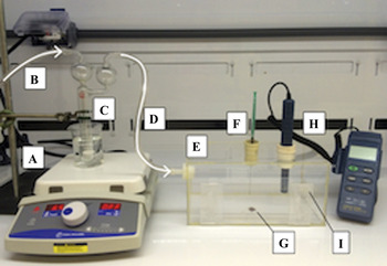
A humidity controlled acrylic chamber, shown in Fig. 2, was constructed for the formation of BFs films (Fig. 2). A 15 mg/mL solution of PS in chloroform, containing 0, 0.02, or 0.1% w/v DBSA, was prepared. Using a plastic syringe, 0.1 mL solution was applied to a 2 cm × 2 cm silicon substrate with a 300 nm thermally grown oxide and an OTS monolayer, formed using the procedure used by Ito et al. Reference Ito, Virkar, Mannsfeld, Oh, Toney and Locklin45 The relative humidity (RH) in the chamber was maintained between 78 and 82%, and the temperature was kept at room temperature (RT) (23 °C), as measured by using a TECPEL DTM-321 Humidity Temperature Meter (Taipei City, Taiwan). Upon evaporation of the solvent, the substrate with the resulting BFs film was removed from the chamber.
BFs chamber set-up for formation of BFs under static conditions. (A) Hot plate, (B) dry N2 flow into the bubbler, (C) bubbler with water submerged in beaker containing warm water, (D) humid N2 flow out of the bubbler and into the chamber, (E) acrylic chamber for BFs formation, equipped with a sliding door for sample insertion and removal, (F) septum for applying solution to the substrate with a needle, (G) silicon substrate on which the BFs film is formed in the chamber, (H) humidity probe and meter, (I) outlet for the humid air from chamber.

2. Micropatterning of PDMS dielectrics
A 10:1 mixture of PDMS elastomer to cross-linker, mixed for 2 min at 3000 rpm, was spin coated onto the BFs film at 5000 rpm for 5 min at an acceleration of 5000 rpm2 (Laurell Technologies Model WS-650MZ-23NPPB/OND, North Wales, Pennsylvania) to achieve a film thickness between 4 and 5 µm. The film was then placed in a vacuum desiccator to remove any air bubbles from the PDMS. For scanning electron microscopy (SEM) imaging with an FEI XL30 Sirion SEM (FEI Company, Hillsboro, Oregon), porous BFs films on silicon substrates and micropatterned PDMS films on polyethylene terephthalate (PET) were coated with a 14 nm layer of gold. The accelerating voltage was 5 kV.
3. Pressure sensor fabrication
A 1-cm-thick strip of PET with conductive indium tin oxide (ITO) was treated with oxygen plasma (Technics Micro-RIE Series 800, Pleasanton, California) for 45 s at 150 mW power and 200 mTorr oxygen and laminated on the top of the degassed PDMS film. The PDMS film was then peeled off of the silicon substrate and transferred to the flexible electrode. After using chloroform to rinse any PS that may have transferred along with the PDMS, a second identical electrode was laminated over the micropatterned area of the PDMS, perpendicular to the first one.
Thin copper strips (0.25 cm wide), to which wires were soldered, were adhered to the ends of the flexible electrodes using a conductive tape. The fully assembled pressure sensor was immobilized on a rigid glass slide and placed beneath a motorized metal probe. A small glass square (0.4 cm × 0.5 cm) was placed on the top of the overlapping ITO region of the electrodes to allow for even application of force over that area. Capacitance was measured by using an Agilent E4980A Precision LCR Meter (Santa Clara, California), and the force applied to the pressure sensor by the metal probe was measured using a force gauge (Mark-10 Model BG05, Copiague, New York). Five cycles of pressure were applied, from 0 to 100 kPa, with the four latter cycles used for analysis of sensor performance.
III. RESULTS AND DISCUSSION
A. BFs fabrication of microporous molds for dielectrics
The first step in the fabrication of the microstructured pressure sensor dielectrics is the formation of porous films to be used as negative templates for molding the dielectric films via soft lithography. The BFs method presents a simple, self-assembly-based process for producing porous films. Since the resulting film morphology is strongly dependent on experimental conditions, several variables can be adjusted to give the optimal conditions for reliably producing porous films with the desired geometrical and physical properties for dielectric molds.
A unique chamber was constructed for the formation of BFs films (Fig. 2). Holes on opposite sides of the chamber provide an inlet and an outlet for humid airflow (D and I), and one on the top is used to insert a hygrometer for monitoring humidity (H). Polymer solution is applied to the substrate via a syringe inserted through a rubber septum on the top of the chamber (F). Humidity is provided to the chamber by flowing nitrogen or air through a bubbler containing water (B–D). Submerging the bubbler in a beaker of warm water increases the vapor pressure of the water inside, allowing the humidity in the chamber to reach values above 80% RH.
As described above, the polymer, solvent, solution concentration, humidity, and additives used in the BFs method affect the formation of porous structures.
Linear PS (MW ∼ 192,000 g/mol) was selected as the polymer for producing honeycomb-structured molds for PDMS dielectrics, as it is inexpensive and has been widely used in the literature to form BFs films. Reference Peng, Han, Yang and Li40,Reference Thong, Lim, Ahsan, Goh, Xu and Chin46–Reference Zheng, Kubowaki, Kashiwagi and Miyazaki48 Research over the last decade has produced ordered structures in linear PS by adjusting the solvent and substrate, and by adding nanoparticles or surfactants to stabilize the templating water droplets. Reference Sun, Shao and Ji21,Reference Stenzel, Barner-Kowollik and Davis49
Chloroform (CHCl3) proved to be the most reliable solvent for the formation of PS BFs, agreeing with several prior studies which found it to be the most robust for forming ordered porous structures on a variety of substrates and over a range of conditions. Reference Xu, Wang, Bian, Wang, Wang, Luo and Dong4,Reference Ferrari, Fabbri and Pilati36,Reference Peng, Han, Yang and Li40,Reference Escalé, Rubatat, Billon and Save50
Increased polymer concentration results in smaller pores due to the increased rate of polymer precipitation and the ability of a greater quantity of polymer molecules to stabilize a larger surface area of water droplets. Reference Hernández-Guerrero and Stenzel18,Reference Pitois and Francois38–Reference Peng, Han, Yang and Li40,Reference Stenzel, Barner-Kowollik and Davis49,Reference Han, Tian, Wang and Xiao51,Reference Huh, Jung, Park, Kang, Nah, Russell, Holden and Yun52 A concentration of 15 mg/mL was used herein for the fabrication of honeycomb-structured dielectric molds, as lower concentrations led to greater droplet coalescence and irregularity in pore size, and higher concentrations produced regions with very small or no pores due to rapid film formation and greater viscosity.
Films were formed at humidities ranging from 70 to 90% RH. A RH of approximately 80% consistently produced close-packed, ordered BFs arrays. Lower humidities often resulted in smaller, more spread out pores, while higher humidities resulted in significant water droplet coalescence and adjoined pores, agreeing with past findings. Reference Hernández-Guerrero and Stenzel18,Reference Maruyama, Koito, Nishida, Sawadaishi, Cieren, Ijiro, Karthaus and Shimomura35 Films were formed at humidities ranging from 70% RH to 90% RH. A RH of approximately 80% consistently produced close-packed, ordered BFs arrays. Lower humidities often resulted in smaller, more spread out pores, while higher humidities resulted in significant water droplet coalescence and adjoined pores, agreeing with past findings. Reference Hernández-Guerrero and Stenzel18,Reference Maruyama, Koito, Nishida, Sawadaishi, Cieren, Ijiro, Karthaus and Shimomura35 Temperature influences BFs formation by affecting the rates of solvent evaporation and water condensation; for example, at a higher temperature, faster solvent evaporation and slower water droplet condensation results in smaller pores. Reference Hernández-Guerrero and Stenzel18,Reference Muñoz-Bonilla, Fernández-García and Rodríguez-Hernández53 Additionally, temperature affects solution viscosity, solubility, and polymer precipitation. Reference Hernández-Guerrero and Stenzel18,Reference Muñoz-Bonilla, Fernández-García and Rodríguez-Hernández53 All BFs experiments herein were conducted at RT (23 °C), as the desired structures could be fabricated and tuned using the various other parameters.
Varying the amount of polymer solution applied to the substrate also affects the resulting porous structures. There is an observed trade-off between achieving structures over a larger area by using a greater volume of solution, and having regular close-packed structures, since more solvent takes more time to evaporate, resulting in larger pores and more irregular structures. Reference Bunz19 While larger patterned areas are desirable for eventual scale-up and for selecting a successfully patterned region for pressure sensor fabrication, they also show greater variation in pore size. Thus, most of the films fabricated were cast from a solution volume of 0.1 mL and had a final diameter of between 1 and 2 cm, depending on the surface wettability of the solvent and the exact amount of solution applied.
To mediate BFs formation, the surfactant was added in small quantities to the PS/CHCl3 solution. Amphiphilic molecules stabilize the templating water droplets through associations between the hydrophilic portion and the water droplets, and between the hydrophobic portion and the CHCl3. Reference Sun, Li and Wu43,Reference Jiang, Zhang, Xu, Wang, Zhou and Gu44 By reducing surface tension between the two phases, less energy is required to maintain a high interfacial surface area between the water and CHCl3, favoring many close-packed pores. Reference Maruyama, Koito, Nishida, Sawadaishi, Cieren, Ijiro, Karthaus and Shimomura35
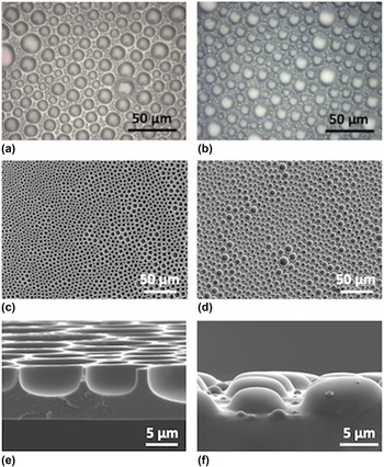
The most reliable formulation for the fabrication of ordered, regular porous structures was found to be a 15 mg/mL PS solution in CHCl3 with the addition of 0.1% w/v DBSA. DBSA was also added at a concentration of 0.02% w/v, but the resulting structures were less consistent within individual films, as well as from film to film. 0.1% DBSA consistently produces what are herein referred to as “interspersed” patterns, with smaller pores filling the areas between larger pores [Fig. 3(a)]. Such interspersed structures, which have not, to our knowledge, been previously reported, likely result from the coalescence of some water droplets and the stabilization of several smaller ones in between by surfactant molecules. While the films are polydisperse, the pores had two distinct length scales, with larger ones ranging in diameter from 10 to 20 μm and smaller ones ranging from 2 to 5 μm.
BFs films and their PDMS replicas. (a) Optical microscopy image of the PS BFs film cast from solution containing 0.1% w/v DBSA, sodium salt (500×). (b) Optical microscopy image of the PDMS film molded from the PS film shown in (a) (500×). (c) Top-view SEM image of the BFs film cast from 15 mg/mL PS in chloroform with 0.1% w/v DBSA (1000×). (d) Top-view SEM image of PDMS molded from the PS film cast under the same conditions as in (c) (1000×). (e) Cross-sectional SEM image of the same film as (c) (10,000×). (f) Cross-sectional SEM image of the same PDMS film as (d) (12,000×).

B. Replication of porous structures in PDMS
The porous BFs films were used as molds to microstructure PDMS via soft lithography to pattern dielectric layers for capacitive pressure sensors. After spin coating a thin film of PDMS onto the BFs film, a flexible PET electrode with a thin strip of conductive ITO was laminated onto the PDMS, and, after curing, peeled off of the substrate to transfer the PDMS.
In addition to influencing the geometry of porous structures, the choice of the substrate for BFs films also affects the adhesion of the polymer film to the surface, which is crucial for proper PDMS spin-coating, molding, and transfer. While ordered BFs structures form on hydrophilic surfaces such as silicon dioxide, the hydrophobic PS films delaminate from them. To ensure adhesion of the PS film onto the substrate, BFs were made on hydrophobic OTS-treated silicon wafers. OTS's hydrophobicity is such that the PS film remains on the substrate prior to PDMS molding, but peels off with PDMS during subsequent transfer. By transferring the film along with PDMS, it is ensured that the microstructures are completely intact on the electrode, and the remaining PS film can be easily rinsed off with CHCl3 without affecting the PDMS. The OTS treatment furthermore improves wetting of the polymer solution on the substrate during BFs formation, which aids in the formation of ordered BFs. Reference Ferrari, Fabbri and Pilati36,Reference Cheng, Tian, Shi, Tang and Xi41,Reference Muñoz-Bonilla, Fernández-García and Rodríguez-Hernández53,Reference Li, Wang, Zhang, Tan, Yu, Zhao, Chen and Xu54 Even though the above process does not allow for repeated use of the PS mold, we found it much more reproducible, and the simple fabrication of the PS mold makes it feasible. Alternatively, further investigation on a suitable substrate treatment should allow for reuse of the PS mold.
Before placing another flexible electrode above the microstructured PDMS and testing the resulting pressure sensor, successful PDMS molding and film transfer had to be confirmed. To better determine the structure of the PDMS films, the extent to which they truly replicate their BFs inverses, and the quality of their transfer, microstructured PDMS films on ITO/PET, as well as their mater PS films, were imaged via optical and SEM (Fig. 3). Figure 3(b) shows a PDMS film molded from the PS film in Fig. 3(a). Comparison of the two films confirms that the integrity of the microstructure geometries has been preserved, with both larger and smaller interspersed structures replicated in the PDMS.
Figures 3(c) and 3(e) show top-view and cross-sectional SEM images of a PS BFs film. In Fig. 3(c), long-range order can be observed in the BFs film, whose pores range from 5 to 10 μm in diameter. Only a few small, interspersed pores formed between these relatively larger ones. It is noted, however, that other areas of the same film closer to its center did contain interspersed pores such as those shown in Fig. 3(a).
Cross-sectional images of the PS film with an angled view of its surface show some of these interspersed pores and confirm the desired pore geometry [Fig. 3(e)]. The pores are roughly hemispherical, suggesting that templating water droplets during BFs formation were approximately half submerged. Solution concentration, polymer, and solvent could have been adjusted to make pores shallower and more open, or deeper and more closed at the top. Reference Escalé, Rubatat, Billon and Save50,Reference Wang, Mao, Wang, Qu, Yang and Hu55,Reference Li, Zhong, Li, Gong, Ben, Xu, Chen and Ma56 The pore depths measured across various BFs are comparable to the sizes of pyramidal microstructures previously used in pressure sensors, which had heights of 6 (Ref. Reference Mannsfeld, Tee, Stoltenberg, Chen, Barman, Muir, Sokolov, Reese and Bao13) and 34 μm. Reference Tee, Chortos, Dunn, Schwartz, Eason and Bao15 Assuming that the radius of BFs pores from top-view optical microscopy images is equal to their depth and the height of the corresponding PDMS microstructures, the heights of the fabricated PDMS microstructures range from 2 to 15 μm.
Top-view SEM images confirm high fidelity of replication of the porous structures, with the PS and PDMS films showing identical microstructure geometries [Figs. 3(c) and 3(d), respectively] and no defects from the transfer. The cross-sectional image in Fig. 3(f) also confirms successful PDMS molding, as the domed microstructures have the same shapes as their PS inverses. Their somewhat flattened tops match the flattened bottoms of the pores shown in Fig. 3(e), indicating that PDMS completely filled the pores following spin-coating. Additionally, the uniform heights of the larger PDMS microstructures imply that the BFs pores were similarly uniform in size and depth.
The presence of smaller domes between the larger ones indicates that PDMS also filled the interspersed pores in the PS film. Such regular multi-length-scale microstructures would be more challenging to produce in a single-step process using the photolithographic and etching methods previously used to create inverse pyramids in silicon, presenting a significant improvement in PDMS dielectric microfabrication.
C. Pressure sensors with BFs-molded microstructured dielectrics
Microstructured dielectric films on ITO/PET electrodes were incorporated into capacitive pressure sensors. Pressure–response curves were obtained by plotting the relative capacitance (ΔC/C 0) versus applied pressure (in kPa). Four of five cycles of application and release of pressure are shown in the graphs, since the first cycle was required to ensure proper lamination of the upper electrode. While testing more cycles would be important in ensuring the long-term stability of the pressure sensors, their reproducibility depends mainly on the mechanical properties of the elastomeric dielectric layer, which can be readily tuned with the use of different materials or cross-linking densities. The “lower” curve in the graphs shows the relative capacitance during application of pressure, and the “upper” during release, with the difference between the two resulting from hysteresis in the PDMS film. As such, hysteresis can be quantified by calculating the greatest difference in pressure, or separation, observed between the pressure application and release curves.
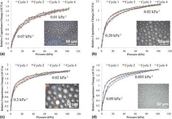
Figure 4 shows the pressure–response curves obtained for four representative pressure sensors, along with optical microscopy images of their PDMS dielectrics. The sensitivities in the low-pressure and medium-pressure regimes are shown on the graphs, and are given by the slope of the curve in those regions, which indicates how rapidly the relative capacitance responds to an incremental increase in pressure. The devices are presented and discussed in order of the most linear pressure response to the least linear response over the entire 100 kPa range, with higher linearity corresponding to a lower loss in sensitivity as pressure is increased (Table I).
Pressure–response curves of sensors with microstructured PDMS dielectrics. Four capacitive pressure sensors containing different microstructured PDMS dielectric films, shown in the inlaid images (500× magnification), were each tested over five cycles, with results for the latter four shown. The pressure sensors are arranged from most linear to least linear, with sensitivity losses of 86% (a), 90% (b), 90% (c), and 99% (d) over the entire 100 kPa range, and from least to greatest amount of hysteresis in the pressure response (see Table I for numerical values). Sensitivities in the low-pressure (<20 kPa) and medium-pressure (>20 kPa) ranges are shown in the graph, and are equal to the slope of the relative capacitance versus pressure curve.

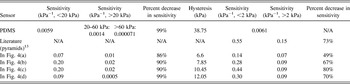
Sensitivities in the medium-pressure range (10–100 kPa, left hand side) and low-pressure range (below 10 kPa, with sensitivities below and above 2 kPa shown, right hand side) for a control pressure sensor (unstructured PDMS dielectric), a sensor with a pyramidal microstructured dielectric (from Ref. Reference Mannsfeld, Tee, Stoltenberg, Chen, Barman, Muir, Sokolov, Reese and Bao13), and for the four pressure sensors in Fig. 4, presented in order of increased losses in sensitivity and increased hysteresis over the entire 100 kPa range. Sensitivities are calculated from the slope of the pressure–response curve during application of pressure for one of the four cycles. The percent decrease in sensitivity in each pressure range is also given. This value was not calculated for the unstructured PDMS sensor since the sensitivity quickly achieved a constant value over the entire range of 0–7 kPa. Hysteresis is calculated by determining the greatest difference in pressure, or separation, observed between the pressure application and release curves.

The pressure sensor in Fig. 4(a) had the most linear response to applied pressure of those shown. Sensitivity decreased from 0.07 kPa−1 below 20 kPa to 0.01 kPa−1 at higher pressures. Below 7 kPa, the pressure sensor showed only 49% decrease in sensitivity, a third less than sensors with pyramidal microstructured PDMS dielectrics reported in the literature, which showed a 73% loss in this range (Table I). Reference Mannsfeld, Tee, Stoltenberg, Chen, Barman, Muir, Sokolov, Reese and Bao13 This greater linearity may be attributed to the highly irregular microstructures in the film, which here range from 3 to 16 μm in diameter (Fig. S2). We previously reported that incorporating differently sized pyramidal microstructures resulted in a longer initial linear range, and that pressure sensor sensitivity can be tuned by incorporating microstructures of varying sizes. Reference Tee, Chortos, Dunn, Schwartz, Eason and Bao15 It is possible that when dielectrics contain less uniform microstructures, only the tallest are initially compressed, and gradually, as they are flattened, other smaller ones begin to compress, leading to greater sensitivity at these higher pressures relative to dielectrics whose structures are compressed simultaneously.
The improved performance of the fabricated sensors relative to those with pyramid-patterned dielectrics may also be due to the hemispherical geometry of the PDMS microstructures. Pyramids are much more sensitive at their tips, where there is minimal contact area with the top electrode, whereas domes would be less sensitive initially, given their rounded structure, and flatten more gradually. In both, as contact area increases, the pressure exerted on the microstructures is reduced, and they being to respond more like a sensor with an unpatterned PDMS dielectric. Reference Tee, Chortos, Dunn, Schwartz, Eason and Bao15 This can explain why most of the pressure sensors approach a similar value for sensitivity at higher pressures: Already at 7 kPa, the sensitivities of the sensors in Fig. 4 fall between 0.07 and 0.09 kPa−1, and as applied pressure nears 100 kPa, the sensitivities approach values of 0.01–0.02 kPa−1 as the structures are more fully compressed [with the exception of the sensor in Fig. 4(d)].
The sensor in Fig. 4(a) showed high reproducibility of pressure sensitivity and the least hysteresis of the sensors discussed here. It is expected that the aspect ratio, or height-to-width ratio, of the microstructures is related to the extent of hysteresis in the pressure response. The results obtained suggest that domes with higher aspect ratios, as indicated by lighting and focus in optical microscopy images, lead to less hysteresis than flatter, low-aspect-ratio structures, which more quickly approach the behavior of bulk, and unpatterned PDMS, resulting in significantly greater hysteresis (Table I).
The structures in Fig. 4(a) appear to have higher aspect ratios, indicated by shadows at the bases of the domes and by the difference in focus between the smaller and larger domes. Higher aspect ratio structures would result from deeper pores in the original PS BFs film. The addition of some surfactant (0.02% w/v DBSA) in the formation of the mold for this film helped stabilize the template water droplets, reducing surface tension and allowing them to submerge deeper into the polymer solution. This amount of DBSA was not enough, however, to produce the interspersed pores that form with 0.1% w/v DBSA.
More significantly, the film contains mostly smaller structures with spread-out clusters of larger domes. As a result, there is a greater amount of air in between the electrodes that the PDMS structures can displace upon compression. Less PDMS results in less hysteresis, and more air leads to relatively higher sensitivity at lower pressures, where the smaller domes have not come into contact with the electrode.
The pressure sensor in Fig. 4(b) is closer in linearity to the pyramidal microstructured dielectrics. Below 7 kPa, it has a 67% decrease in sensitivity from 0.28 to 0.09 kPa−1. Over the entire 100 kPa range, average sensitivity decreases an order of magnitude from 0.20 to 0.02 kPa−1 (Table I).
Optical microscopy images show that the structures in the sensor in Fig. 4(b) are also very irregular, ranging from 10 to 26 μm in diameter (or 5–13 μm tall, assuming that dome height is approximately half of the diameter). A histogram showing the distribution of microstructure sizes in the film reveals a relatively even distribution of structures across that size range, similar to the sensor in Fig. 4(a), which would contribute to its having a more linear pressure response compared to that of sensors with more uniform domes or pyramids (Fig. S2). The gradual compression of increasingly smaller domes causes the relative capacitance to change at a more constant rate. This sensor's greater loss in sensitivity than the one in Fig. 4(a) can be attributed to the denser packing of the microstructures in the film, which will more rapidly approach the behavior of bulk PDMS as they are compressed in closer proximity to one another and make contact.
Sensor in Fig. 4(b) also exhibits very little hysteresis, performing nearly identically over all four cycles. The structures appear to have relatively high aspect ratios, from the lighting and focus of the image, supporting the proposed correlation between the aspect ratio and hysteresis in pressure response. The high aspect ratio of the domes is once again a result of their BFs mold having been cast from a solution containing 0.1% w/v DBSA surfactant. Slightly higher hysteresis at intermediate pressures compared to the sensor in Fig. 4(a) could be due to the close packing of structures, which may come into contact upon compression and behave more like unpatterned PDMS.
The pressure sensor in Fig. 4(c) had the same 90% decrease in sensitivity as the one in Fig. 4(b) over the entire 100 kPa range. However, it has the least linear response in the low-pressure regime: at pressures below 7 kPa, the sensitivity decreasing 80% from 0.44 to 0.09 kPa−1. The actual sensitivity values were not far from those of the pyramidal microstructures, though, whose sensitivity dropped from 0.55 to 0.15 kPa−1 over the same range (Table I). Reference Mannsfeld, Tee, Stoltenberg, Chen, Barman, Muir, Sokolov, Reese and Bao13
The dielectric film of the sensor in Fig. 4(c) contains smaller domes (2–10 μm diameter) regularly interspersed between larger ones (19–33 μm diameter) (Fig. S2). This pressure sensor is actually made from a different area of the same PDMS film used in the pressure sensor in Fig. 4(b); however, that other area of the film has smaller pores and no interspersed microstructures since it was molded from a region closer to the edge of the BFs film, where water droplets had less time to grow and coalesce to form larger pores.
The even, bimodal distribution of these microstructures may contribute to the rapid decrease in sensitivity, as the larger domes are all simultaneously compressed, followed by the smaller ones. As the larger ones are compressed, they fill more of the space between the electrodes, which could prevent the top electrode from contacting the smaller domes. That would cause the structures to behave even more like monodisperse, larger domes that, at higher pressures, approach the properties of unpatterned PDMS.
Similar to the microstructures in Fig. 4(b), the domes in Fig. 4(c) also appear to have a high aspect ratio. There are noticeable shadows along the edges of the large domes, and the smaller interspersed structures are in good focus while the larger domes are not. However, it has slightly greater hysteresis than the sensor in Fig. 4(b). This could be due to the presence of unpatterned patches in the PDMS film, which can be seen at lower magnifications (Fig. S1), and would lead to behavior slightly more similar to an unpatterned dielectric. This suggests that hysteresis can be diminished by improving PDMS molding and transfer, or by forming deeper BFs pores with the use of a surfactant, while still maintaining irregularity in porous structures to promote a more linear pressure response.
Finally, Fig. 4(d) shows the pressure–response curves for the least sensitive sensor discussed herein. Its sensitivity starts at 0.09 kPa−1 below 20 kPa, dropping 99% to 0.0005 kPa−1 between 40 and 100 kPa. This larger decrease in sensitivity can once again be explained by the highly uniform microstructures throughout the film (mostly between 7 and 9 μm in diameter, though ranging from 5 to 13 μm), which would all be compressed at once, resulting in a rapid loss in sensitivity (Fig. S2).
In the low-pressure regime, the sensor exhibits a 70% decrease in sensitivity, which is actually less than the sensor in Fig. 4(c) (Table I). This is probably because its microstructures are smaller and less densely packed. At low pressures, the larger structures of the sensor in Fig. 4(d) that are initially compressed appear to be more varied in size, which would lead to a more linear response. At higher pressures, however, the highly uniform structures will behave more like unstructured PDMS, whereas the two distinct length scales of domes in the sensor in Fig. 4(c) will lend it greater linearity over the entire 100 kPa range.
The sensor in Fig. 4(d) shows more hysteresis than the other sensors, which could be explained in two ways. First, unpatterned regions in the film may contain unmoved PDMS, which would result in greater hysteresis. Second, the structures seem to have lower aspect ratios, with less noticeable shadows and more even focus, which would result in film properties more similar to bulk PDMS. The shorter microstructures can be explained by the lack of surfactant in the polymer solution used to fabricate the BFs mold for this film, which as a result had shallower pores. These same factors can also explain the sensor's lower sensitivity values.
IV. CONCLUSIONS
The results presented here demonstrate the successful application of the BFs technique as a simple, fast, low-cost, and tunable method for fabricating porous molds for flexible, microstructured dielectrics. Capacitive pressure sensors containing these dielectrics show, for the most part, high sensitivities in the low-pressure regime comparable to previous similar devices. Reference Mannsfeld, Tee, Stoltenberg, Chen, Barman, Muir, Sokolov, Reese and Bao13,Reference Tee, Chortos, Dunn, Schwartz, Eason and Bao15 At both low pressures and higher pressures up to 100 kPa, the BFs-patterned dielectrics produce greater linearity in pressure response, which is important for pressure sensors that mimic the ability of skin to sense a wide range of applied pressures. While the sensors experienced sensitivity losses of 86% or more over the 100 kPa range, previous studies on similar capacitive sensors did not report any pressure sensitivities over such a wide range, and the ability of these devices to sense both low and medium pressures is significant.
Analysis of various sensors' pressure–response curves suggests that less regular PDMS microstructures may lead to a more linear pressure response, as domes are gradually compressed in order of decreasing size, as opposed to the concurrent compression of uniform microstructures that rapidly assume the properties of bulk, unpatterned PDMS films. Thus, the self-assembled structures produced via the BFs method provide ideal templates for improved capacitive pressure sensor dielectrics.
The fabricated pressure sensors have reproducible response to pressure over successive cycles with little hysteresis. By comparing optical microscopy images of the microstructured dielectrics to the pressure–response curves obtained, it is observed that dielectrics with higher-aspect-ratio structures produce less hysteresis. On the other hand, the lower-aspect-ratio or more densely packed structures behave more similarly to unstructured PDMS, and therefore result in greater hysteresis.
Future experiments include optimizing the conditions of BFs formation to produce porous structures that are more polydisperse to promote a more linear pressure response, less densely packed and with high aspect ratios to reduce hysteresis, and that have more consistent geometries over a larger area for eventual scale-up.
Finally, quantitative analyses of images of PS and PDMS films will confirm the suggested qualitative correlations between the dielectric structure and pressure response. Mathematically modeling the compression of domed structures and accurately measuring their sizes and polydispersity will furthermore provide useful insights for improving the process developed herein for fabricating pressure-sensing devices for electronic skin applications.
Supplementary Material
To view supplementary material for this article, please visit http://dx.doi.org/jmr.2015.334.
ACKNOWLEDGMENTS
S.M. acknowledges Stanford Undergraduate Advising and Research (UAR) and the Barry Goldwater Scholarship and Excellence in Education Foundation for support through funding. S.M. acknowledges Alex Chortos, as well as other members of the Bao Group, for sharing useful knowledge and advice.