I. INTRODUCTION
The carrier saturation velocity in silicon carbide (SiC), being higher than that in silicon (Si), has enabled the fabrication of SiC devices that are more energy efficient at high operating voltages than their Si counterparts. Also, the wider band gap of SiC extends the extrinsic behavior range allowing operation at higher temperatures, which, together with the better thermal conductivity, reduces cooling requirements.
However, implementing metal-oxide-semiconductor field-effect transistors (MOSFETs), thereby extending switching capabilities to high frequencies, has proven to be a challenge because of major issues at the oxide/SiC interface. In particular, the high density of charged defect states induces coulombic interactions with the minority carriers and is a major contribution to the scattering mechanisms limiting the channel mobility.Reference Rozen, Ahyi, Zhu, Williams and Feldman1–Reference Arnold and Alok3 Consequently, this region can dominate the ON resistance of oxide-based devices, which prevents SiC MOSFETs from achieving their full potential in terms of energy efficiency.
While it is often pointed out that SiC is the only wide band-gap semiconductor to grow silicon dioxide (SiO2) as a stable thermal oxide, favoring its processing with Si-compatible technology, it turns out that it also yields a large density of interface traps (DIT). Indeed, the complex oxidation process, which involves the release of carbon, makes for an intricate oxide/semiconductor interface.Reference Wang, Dhar, Wang, Ahyi, Franceschetti, Williams, Feldman and Pantelides4–Reference Hijikata, Yaguchi and Yoshida6 To avoid these drawbacks, a lot of effort has been put into either depositing gate dielectrics and/or passivating the interface before/after its formation.
The deposition of a gate dielectric, including alternate materials such as aluminum (III) oxide (Al2O3), has shown promising results, but the presence of a thin thermally grown interface has remained necessary to achieve better performance.Reference Noborio, Suda and Kimoto7–Reference Lichtenwalner, Misra, Dhar, Ryu and Agarwal9 Thus, the same method as for thermal oxides is often employed to reduce DIT with passivating nitrogen atoms (N) at the interface. Several techniques can be used to introduce N, such as implantation, radical nitridation, and annealing in nitrous oxide (N2O) or nitric oxide (NO).Reference Li, Dimitrijev, Harrison and Sweatman10–Reference Zhu, Ahyi, Li, Chen, Rozen, Feldman and Williams13 Of all these techniques, NO annealing has become a reference for the past decade as it minimizes the DIT, which inversely scales with the N amount incorporated. NO yields up to a half monolayer of N at the interface.Reference Rozen, Dhar, Zvanut, Williams and Feldman14 However, this number remains limited by interface regrowth during nitridation and the nitrogen profile extends into the oxide, which generates a large amount of hole traps and jeopardizes the stability of the devices.Reference Rozen, Dhar, Zvanut, Williams and Feldman14
Shirasawa et al.Reference Shirasawa, Hayashi, Yoshida, Mizuno, Tanaka, Muro, Tamenori, Harada, Tokushima, Horikawa, Kobayashi, Kinoshita, Shin, Takahashi, Ando, Akagi, Tsuneyuki and Tochihara15 obtained a silicon nitride (SiN) and silicon oxide (SiO) bilayer on 6H–SiC, that can theoretically exist without dangling bonds, by slightly etching the substrate with hydrogen at high temperature, followed by N2 exposure (a process here called “N2 conditioning”). The 4H-polytype surface chemistry being similar, we expect to form a highly localized N layer, without the need for thermal oxidation, that can be used as a seed for gate oxide deposition if it remains stable during device processing.
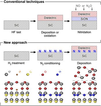
In this article, we propose a route to confine nitrogen to the interface by submitting a 4H–SiC bare surface to N2 conditioning, followed by the deposition of a gate dielectric, as illustrated in Fig. 1. We demonstrate the potential of this new approach by showing that the DIT, from metal-oxide-semiconductor capacitors (MOSCAPs) so fabricated, is reduced to a level that can be even lower than in devices formed with direct oxidation. The nitrogen in the gate stack is characterized by secondary ion mass spectroscopy (SIMS) and x-ray photoelectron spectroscopy (XPS).
Schematic of oxide-semiconductor stacks formed by a conventional process with gate dielectric deposition or oxidation followed by nitridation using NO or N2O annealing, and by a new surface nitridation approach using N2 conditioning followed by the gate dielectric deposition. The bottom drawings are corresponding atomic configurations previously proposed.Reference Shirasawa, Hayashi, Yoshida, Mizuno, Tanaka, Muro, Tamenori, Harada, Tokushima, Horikawa, Kobayashi, Kinoshita, Shin, Takahashi, Ando, Akagi, Tsuneyuki and Tochihara15, Reference Bernhardt, Schardt, Starke and Heinz20

II. EXPERIMENTAL
MOSCAPs were fabricated on chemically cleaned n-type epi-SiC (N doping ≈ 5 × 1015 cm−3) grown along the (0001) direction on commercially available highly doped substrates. The devices were made with either a standard thermal oxide, a standard deposited oxide, a control-deposited oxide on a H2-treated surface, or a deposited oxide on a N2-conditioned surface. Prior to oxide formation, all samples were dipped in buffered hydrofluoric acid (HF). Thermal SiO2 was obtained by oxidation in dry oxygen at 1200 °C. High-temperature deposited oxides (HTO) result from a 4.5 min low-pressure chemical-vapor deposition process (LPCVD) at 0.75 Torr and 900 °C, using a mixture of silane (SiH4) (15 sccm) and nitrous oxide (N2O) (500 sccm). Standard HTO films were deposited on a HF-etched surface. On one hand, for control capacitors, SiO2 was deposited on SiC surfaces, which had been exposed to a high-temperature H2 treatment (10 slm hydrogen for 15 min at 700 Torr). On the other hand, N2-conditioned surfaces were obtained by introducing N2 in the chamber (10 slm nitrogen for 15 min at 700 Torr) following the H2 treatment. The temperature in the reactor was set between 1050 and 1450 °C, remaining constant during H2 treatment and N2 conditioning. The approximate thickness of all oxides was around 50 nm. Top aluminum (Al) electrodes were formed and the back of the substrates were coated with gold (Au).
High-frequency capacitance-voltage (CV) curves, taken at room temperature from accumulation to depletion at 100 kHz, yield DIT via the Terman method.Reference Nicollian and Brews16 In these conditions, the accurate energy window relative to the conduction band edge is expected to be between 0.2 eV, shallower states being able to respond to the AC signal, and 0.6 eV, deeper states being too slow to emit and reach equilibrium with the DC component (0.5 V/s).Reference Dhar, Pantelides, Williams, Feldman, Fleetwood, Pantelides and Schrimpf17 SIMS was performed to track elemental profiles in the gate stacks and detect the presence of nitrogen at the SiO2/SiC interface. XPS measurements used a monochromatic Al kα beam (1486.6 eV) to probe atomic binding energies and signal intensity. To maximize sensitivity, HTO oxides deposited on XPS samples were scaled down to about 2 nm.
III. MATERIALS ANALYSIS
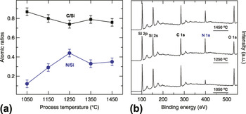
The impact of process temperature on N2 conditioning of bare SiC surfaces can be characterized from the integrated C and N XPS signals relative to Si, as shown in Fig. 2. First, it can be seen that N is indeed incorporated using this method. Second, there is a correlation between the two signals as the amount of nitrogen present at the surface scales with the removal of carbon. This phenomenon will be further discussed later in this section. From these results, we also conclude that N incorporation is thermally activated and is most effective at process temperatures above 1250 °C. Therefore, we have chosen to fix the temperature of this step at 1350 °C during the fabrication of all samples discussed beyond this point.
(a) C to Si and N to Si ratios, resulting from H2 and N2 exposures of clean SiC surfaces at different temperatures. (b) Sample XPS signals used for integration.

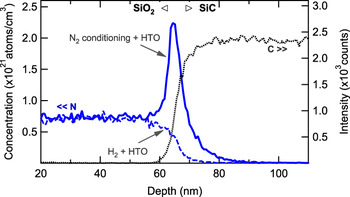
To confirm that N remains at the interface following oxide deposition in the devices fabricated on a nitrogen-conditioned SiC surface, SIMS profiles are plotted in Fig. 3. Note that the background nitrogen in the oxide bulk is identical to what is observed in both the standard and control HTO samples, and is attributed to the deposition process involving N2O. However, a N interface peak is unique to the samples exposed to N2 prior to oxide deposition. From the integration of that peak, the amount of interfacial nitrogen is estimated to be in the 1014–1015 cm−2 range, as observed following other nitridation techniques.Reference Poggi, Moscatelli, Solmi and Nipoti12–Reference Rozen, Dhar, Zvanut, Williams and Feldman14
SIMS profiles showing the accumulation of nitrogen (left axis) at the interface in devices fabricated with a deposited oxide on a SiC surface that has been exposed either exclusively to H2 or to both H2 and N2. The background signal in the dielectric bulk is related to the deposition technique. The carbon profile (right axis) indicates the position of the interface.

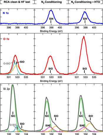
From the scaled XPS spectra shown in Fig. 4, it is found that the N 1s signal forms a single symmetric peak at 397.96 eV, corresponding to Si–N bonds. So the nitrogen resulting from N2 conditioning is exclusively attached to Si atoms, as in trisilicon tetranitride (Si3N4) and silicon oxynitride (SiN2O2), both before and after HTO deposition. This contrasts with observations made in NO-annealed thermal oxides, where C–N bonds are also detected.Reference Li, Dimitrijev, Sweatman, Harrison, Tanner and Feil18 Note that the slight reduction in signal following oxide deposition could be explained by a smaller XPS yield, implying that significant N desorption or migration in the dielectric does not occur. The interfacial N density detected by XPS agrees well with the aforementioned SIMS data. The O 1s spectra show that in all cases oxygen is bonded exclusively to silicon. The peak at 532.79 eV results from Si atoms in SiO2, while the peak at 532.4 eV, observed only in HF-last samples, can be attributed to adsorption of oxygen atoms and hydroxyl groups forming a substoichiometric oxide layer on the surface.Reference Amy, Soukiassian, Hwu and Brylinski19 Other configurations, such as C–O and N–O bonds, can be excluded because they would result in a signal at higher energy. Finally, the Si 2p spectra can be deconvoluted into three components, which include the bulk SiC and oxide signals at 100.96 and 103.00 eV, respectively. The third peak at 101.94 eV observed after HF dip is attributed to lower Si oxidation states from the substoichiometric surface layer. After N2 conditioning, the nitride component (Si–N bonds) is found at 101.66 eV.
XPS spectra (a.u) from three sample types: cleaned surface dipped in HF (left), N2-conditioned surface (center), and HTO on a N2-conditioned surface (right). The N 1s (top), O 1s (middle), and Si 2p(bottom) signal intensities are plotted, on the same scale, as a function of binding energies.

The origin of oxygen atoms seen in comparable amounts after H2 treatment and N2 conditioning remains to be determined. It could be related to residual oxygen in the chamber or to ex situ characterization. In any case, the intensity and components of the XPS signal suggest that neither significant oxidation nor formation of additional defects occur. The density of oxygen atoms observed is consistent with monolayer SiO coverage implied by previous studies.Reference Shirasawa, Hayashi, Yoshida, Mizuno, Tanaka, Muro, Tamenori, Harada, Tokushima, Horikawa, Kobayashi, Kinoshita, Shin, Takahashi, Ando, Akagi, Tsuneyuki and Tochihara15, Reference Bernhardt, Schardt, Starke and Heinz20 The presence of a top oxide layer, which forms without compromising the nitrided interface, yields however an appealing seed layer for subsequent deposition.
In Fig. 1, epitaxial structures compatible with our observations were drawn. They were proposed by Bernhard et al. and Shirasawa et al.Reference Shirasawa, Hayashi, Yoshida, Mizuno, Tanaka, Muro, Tamenori, Harada, Tokushima, Horikawa, Kobayashi, Kinoshita, Shin, Takahashi, Ando, Akagi, Tsuneyuki and Tochihara15, Reference Bernhardt, Schardt, Starke and Heinz20 Following the H2 treatment, Si–O–Si bridges are thought to form a hexagonal lattice, leaving a silicon atom terminated by hydrogen at the center of each hexagon.Reference Tsuchida, Kamata and Izumi21 The structure remains similar following N2 conditioning but each upper most carbon atom is replaced by 3-fold coordinated nitrogen, while the lone silicon is removed. This substitution of C by N is consistent with the trend showed in Fig. 2(a) as the N2 conditioning process temperature was progressively increased. A larger change in the N/Si ratio can be explained by the sensitivity of the XPS signal to the top surface where N atoms are incorporated, while the C/Si ratio also contains a large bulk component. To characterize the transition from a H2-treated surface to a N2-conditioned surface, the evolution of atomic ratios, extracted from XPS data taken on samples processed at 1350 °C, was tracked. We conclude that if the oxygen signal taken as a reference is constant, the ratios of C removed per N incorporated |ΔC/ΔN| = 0.97 and of Si removed per N incorporated |ΔSi/ΔN| = 0.41. These values are close to the ratios 1/1 and 1/3, respectively, expected if there is indeed a transition between the two atomic structures illustrated in Fig. 1 in which all top C atoms are replaced by N, while only the central substrate Si atom below each hexagonal oxide cell is emitted.
IV. ELECTRICAL PROPERTIES
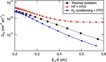
Figure 5 shows typical normalized CV curves measured on three types of MOSCAPs. The relative shift of the curves depends both on the effective positive fixed charge and on the density of electrically active defects in the upper part of the semiconductor band gap. The DIT contribution between 0.2 and 0.6 eV from the SiC conduction band edge is shown in Fig. 6. As expected, the defect density at the SiO2/SiC interface is higher in the standard deposited oxide when compared with the standard thermal oxide. However, the quality of the interface of capacitors with a deposited oxide on a N2-conditioned surface is greatly improved, and even slightly better than the one of the thermal oxide. This trend is confirmed by the peak values of the conductance, also plotted in Fig. 5. Because the DIT of the control deposited oxides on H2-etched surfaces (not shown) is identical to the DIT of the standard deposited oxides on HF-etched surfaces, the DIT reduction is clearly associated with the high-temperature N2 exposure.
Normalized capacitance and conductance curves as a function of bias from devices with a standard thermal oxide, a deposited oxide on a standard HF-etched surface, and a deposited oxide on a N2-conditioned surface. The latter configuration yields an improved interface. The conductance data corresponding only to the depletion regime, where leakage is negligible, is shown to highlight peak values proportional to DIT.

Density of interface states, as a function of energy relative to the conduction band edge, extracted from the data shown in Fig. 5, confirming the improvement induced by the N2 conditioning process.

The introduction of nitrogen at the interface indeed correlates with the observed reduction of electrically active defects. The novelty of the nitridation technique employed here is that a nitrided interface of comparable or even better quality than in the case of thermal SiO2 can be obtained without the need for oxidation, therefore avoiding the formation of induced oxide and SiC bulk defects. It is however important to recognize that although the DIT shown here hints at an improvement, it still does not reach NO-like levels under the studied conditions. But again, unlike other passivation processes, N2 conditioning offers the perspective to maximize and localize incorporated nitrogen without generating electrically active defects. It should accordingly be further explored by tweaking the nitridation step and the oxide deposition temperature that needs to be low enough to prevent depassivation or thermal oxidation, and high enough to obtain a quality dielectric. Indeed, the integrity of the oxide itself do weigh in heavily on the density of states at the interface formed on the 4H-polytype, which likely limits the DIT reduction reported here. Oxide and interface quality should be optimized in parallel to maximize the benefits of the conditioning technique over post-oxidation annealing. Therefore, other deposition techniques and alternate materials should be considered, so that the impact on the integrity of the interface and the oxide is minimized. The nitrided interface will then be expected to translate into higher inversion mobility. Not only because of a reduction of coulombic scattering, but also because gentle passivation yields a smoother oxide/semiconductor interface, as surface-roughness scattering dominates at high transversal fields.Reference Bernhardt, Schardt, Starke and Heinz20, Reference Sieber, Seyller, Ley, James, Riley, Leckey and Polcik22, Reference Tilak, Matocha and Dunne23
V. CONCLUSIONS
To conclude, we observe the reduction of electrically active defects following N2 conditioning of the SiC surface, which generates Si–N bonds prior to oxide deposition, using a combination of H2 and N2 exposure at 1350 °C. The DIT reduction, a smoother interface, and the deposition of a quality dielectric are expected to notably increase the mobility if the process can be optimized so that a maximum of N atoms are present at, and confined to, the dielectric/semiconductor interface formed without any oxidation.