
Introduction
Since Fujishima and Honda discovered photoelectrochemical water splitting with n-type TiO2 electrodes in 1972,[Reference Fujishima and Honda1] overwhelming attention has been focused on photoelectrolysis of water to oxygen and hydrogen in the past decades[Reference Bolton2–Reference Song, Kim, Lee, Cho, Cha, Jeong, An, Kim, Jung, Park, Jung, Kim, Jo, Bu, Jang and Lee10] due to the increasing demand on sustainable energy supply and environmental protection.[Reference Wang, Tadé and Shao11, Reference Seh, Kibsgaard, Dickens, Chorkendorff, Nørskov and Jaramillo12] The solar energy-based water splitting is one of the attractive technologies to prevent environmental pollution and overcome the global energy crisis[Reference Dunn13–Reference Kwon, Choi, Hong, Andoshe, Suh, Kim, Choi, Oh, Kim and Jang16] owing to its non-toxicity and sustainability. Photoelectrochemical water splitting is a carbon-free reaction that reduces water to hydrogen in photocathode and oxidizes water to oxygen in photoanode. Among the two cathodic and anodic reactions that take place in each electrode, photoanodic water oxidation is particularly challenging and requires high overpotentials due to the slow kinetics with multi-electron transfer.[Reference Lewis and Nocera17, Reference Kanan and Nocera18] Thus, research on photoanode that can oxidize water to oxygen in a stable way is crucial for commercially available photoelectrochemical cells (PECs).
Water oxidation in photoanode involves multiple steps including light absorption, charge separation, transportation, and charge injection to water.[Reference Henderson19–Reference Ma, Wang, Jia, Chen, Han and Li22] Therefore, desirable photoanodes should have a properly small band gap to absorb sunlight and generate electron–hole pair, sufficient carrier lifetime and efficient charge separation to suppress recombination, and thermodynamically favorable valence band edge position that provides sufficient overpotential for charge injection to water.[Reference Park, McDonald and Choi23] In principle, TiO2 can only utilize <5% of the solar energy due to the wide bandgap (3–3.2 eV), which restricts its potential application. Thus, as an alternative, various n-type semiconductors have been investigated with these requirements.[Reference Khan and Akikusa3, Reference Akikusa and Khan5, Reference Song, Cha, Lee, Jeong, Seo, Yoo, Kim, Lee, No, Kim, Jeong, An, Lee, Bark, Park, Jang and Lee9, Reference Song, Kim, Lee, Cho, Cha, Jeong, An, Kim, Jung, Park, Jung, Kim, Jo, Bu, Jang and Lee10, Reference Kanan and Nocera18, Reference Zou, Ye, Sayama and Arakawa24] Among them, bismuth vanadate (BiVO4) has been known as one of the promising materials for water oxidation with the proper valence band edge position located at near 2.4 eV versus reversible hydrogen electrode (RHE).[Reference Xie, Zhang, Cai, Qiu and Xiong25] In addition, BiVO4 has many advantages for water oxidation such as appropriate band gap (2.4 eV) for visible light absorption, earth abundance, low cost, and good photostability.[Reference Prévot and Sivula26–Reference Abdi, Han, Smets, Zeman, Dam and van de Krol28] The effective masses of charge carriers in BiVO4 are also calculated to be much lighter than those of other photoactive materials such as TiO2 and In2O3.[Reference Zhao, Li and Zou29, Reference Walsh, Yan, Huda, Al-Jassim and Wei30] The theoretic maximum photocurrent density of BiVO4 is evaluated to be 7.5 mA/cm2 under standard sunlight and the corresponding solar-to-hydrogen conversion efficiency reaches up to 9.2%.[Reference Prévot and Sivula26] To date, however, practical conversion efficiency of BiVO4 materials is far below than the expected value, because of the excessive electron–hole recombination, slow charge transportation, and poor water oxidation kinetics. Therefore, numerous strategies have been progressed to overcome the drawbacks and limitations for commercial use of BiVO4 in solar water splitting.
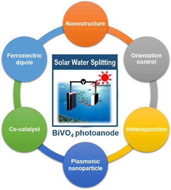
Herein, we focus on the strategies to design and fabricate highly efficient BiVO4 photoelectrodes for water oxidation. Various approaches such as morphology control, orientation control, constructing heterostructures, utilizing plasmonic effects, co-catalyst loading, and control of interface band bending with ferroelectrics are introduced. The most up-to-date techniques, ideas, concepts, and insights to increase the water-splitting performance of the photoanode material are contained in this article that are applicable to other photoelectrodes.
Strategies for highly efficient bismuth vanadate photoanode
The major limiting factors of BiVO4 are (1) significant recombination of electron and holes, (2) poor electrical conductivity, and (3) a slow hole injection rate of water for water oxidation.[Reference Zhong, Choi and Gamelin31–Reference Su, Guo, Bao and Grimes34] Following strategies are to address one or more limitations of BiVO4 and how these attempts affect the photoelectrochemical performance of BiVO4 is discussed.
Morphology control
Nanostructured materials can provide large surface areas, abundant surface states, and diverse reaction sites compared with the bulk materials.[Reference Tong, Ouyang, Bi, Umezawa, Oshikiri and Ye20] Various attempts have been made to develop novel nanomaterials in recent years.[Reference Kamat35–Reference Chen and Mao38] However, increasing surface area-to-volume ratio is not always the result in the higher efficiency but gives rise to adverse effects since extra defect sites which can act as recombination sites are also created in the surface.[Reference Berglund, Flaherty, Hahn, Bard and Mullins39] Therefore, fine control to optimize photoelectrochemical property of nanostructured BiVO4 is needed.[Reference Choi40]
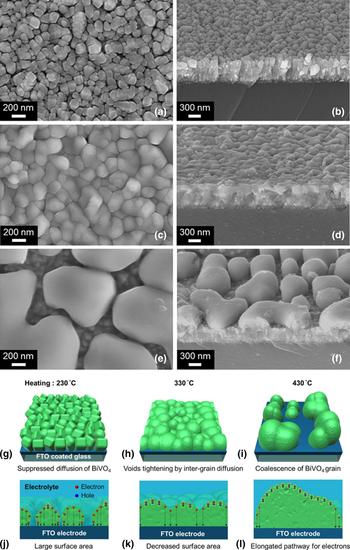
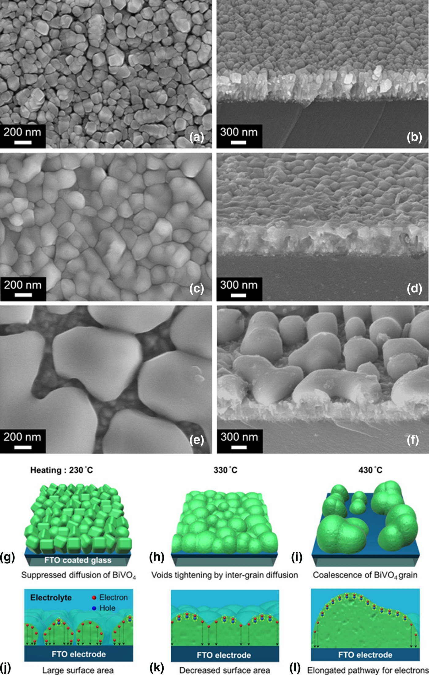
Nanostructured BiVO4 can be grown by various methods such as metal–organic decomposition,[Reference Zhong, Choi and Gamelin31, Reference Chen, Manser and Kamat41] electrodeposition,[Reference Seabold and Choi42, Reference Xiao, Chen, Yang, Long, Wang, Zhu, Qu and Yang43] chemical vapor deposition,[Reference Alarcón-Lladó, Chen, Hettick, Mashouf, Lin, Javey and Ager44] molecular beam epitaxy,[Reference Stoughton, Showak, Mao, Koirala, Hillsberry, Sallis, Kourkoutis, Nguyen, Piper, Tenne, Podraza, Muller, Adamo and Schlom45] and pulsed laser deposition.[Reference Rettie, Mozaffari, McDaniel, Pearson, Ekerdt, Markert and Mullins46, Reference Van, Chang, Chen, Tsai, Tzeng, Lin, Kuo, Liu, Der Chang, Chou, Wu, Chen, Luo, Hsu and Chu47] Jeong et al. prepared high-quality and porous BiVO4 thin film by a pulsed laser deposition method.[Reference Jeong, Choi, Shin, Kim, Song, Yoon, Jang, Yoon, Jeon, Lee and Lee48] Low-temperature growth of pulsed laser deposition would bring about a three-dimensional island growth (the Volmer–Weber growth).[Reference Ashfold, Claeyssens, Fuge and Henley49] Three different films with different surface morphologies are synthesized by controlling the deposition temperature as shown in Fig. 1. The substrate was heated to 230, 330, and 430 °C. Microstructures of the BiVO4 grains show significant change with the deposition temperature. As grain size increases with increasing the deposition temperature, surface area decreases. Vertically arranged BiVO4 grains are individually separated in Figs. 1(a) and 1(b), which is deposited at 230 °C. In Figs. 1(c) and 1(d), the film has larger grain size and smooth surface morphology since diffusion of BiVO4 is promoted while deposition at 330 °C. When the film is deposited at 430 °C, grains are coalesced and result in the formation of largest grain and the exposure of underlying F-doped tin oxide glass layer, which is shown in Figs. 1(e) and 1(f). The thickness of the film deposited at 430 °C is about 400 nm. Photocurrent density of the film deposited at 230 °C is substantially enhanced to have 3.0 mA/cm2 at 1.23 V versus RHE with a hole scavenger where the film deposited at 430 °C exhibited 0.72 mA/cm2 at 1.23 V.[Reference Jeong, Choi, Shin, Kim, Song, Yoon, Jang, Yoon, Jeon, Lee and Lee48] Photogenerated electrons can easily travel to the bottom electrode as depicted in Fig. 1(j), which results in the increase of carrier lifetime of generated holes and thus the rise of the photocurrent density. With the higher process temperature, grains are getting larger, causing the decrease of surface area. In addition, photogenerated electrons cannot reach the bottom electrode and recombine with holes, giving rise to the decrease of photocurrent density.
Top and cross-sectional SEM images of BVO films deposited at (a, b) 230 °C, (c, d) 330 °C, and (e, f) 430 °C. Schematic diagram of process temperature effect on (g–i) morphology change and (j–l) its charge collection abilities. Reproduced with permission from Ref. Reference Jeong, Choi, Shin, Kim, Song, Yoon, Jang, Yoon, Jeon, Lee and Lee48. American Chemical Society Publications, 2017.
Kim and Choi demonstrated that electron–hole separation yield of nanoporous BiVO4 can effectively be increased without additional doping when the electrode is composed of nanoparticles (NPs) smaller than its hole diffusion length.[Reference Kim and Choi50] Mean particle size was about 76 ± 5 nm, which is smaller than reported hole diffusion length of BiVO4, 100 nm,[Reference Rettie, Lee, Marshall, Lin, Capan, Lindemuth, McCloy, Zhou, Bard and Mullins51] creating a three-dimensional nanoporous network as shown in Fig. S1. Onset potential of the nanoporous BiVO4 was 0.1 V versus RHE and photocurrent density at 1.23 V was about 4.5 mA/cm2 with a hole scavenger. Electron–hole separation yield has also been calculated by considering photocurrent density, photon absorption rate, and hole injection yield.[Reference Kim and Choi50] Calculated electron–hole separation yield was about 0.90 ± 0.03 at 1.23 V versus RHE, which is noteworthy as a typical value for BiVO4 electrodes is below 0.6 at 1.23 V versus RHE.[Reference Abdi, Han, Smets, Zeman, Dam and van de Krol28, Reference Zhong, Choi and Gamelin31, Reference Abdi and van de Krol32]
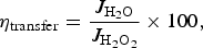
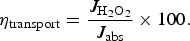
Kang et al. fabricated nanodome-structured BiVO4/GaON bilayer for photoanode.[Reference Kang, Han, Baek, Lee, Song, Bin Kwon, Cho, Jung and Yoon52] BiVO4/GaON forms type I heterojunction. The large energetic barrier of valence band minimum in the GaON would act as a hole mirror and blocks holes to be transferred from BiVO4 to GaON. Subsequently, holes will move to the surface of the BiVO4 layer and participate in oxidizing electrolyte,[Reference Alarcón-Lladó, Chen, Hettick, Mashouf, Lin, Javey and Ager44] while electrons recombine at the interface since GaON has large surface defects which can act as recombination sites.[Reference Iqbal, Khan, Yamani and Qurashi53] To fabricate the BiVO4/GaON nanodome structure, firstly, GaON nanospheres are deposited on the F-doped tin oxide glass substrate, and 50 nm-thick BiVO4 layer is coated on the surface of GaON nanospheres to form a nanodome-structured bilayer photoanode as shown in Fig. S2(e). Nanodome-structured BiVO4/GaON heterostructure (ND-BVO/GaON) has slightly enhanced the light absorption property (75%) compared with the planar BiVO4/GaON heterostructure (P-BVO/GaON, 71% light absorption) and bare BiVO4 photoanodes (62% light absorption). With these two features, type I junction and improved light absorbance, BiVO4/GaON bilayer photoanode has enhanced charge separation and increased photocurrent generation. It is obvious that nanostructured BiVO4 exhibits higher photocurrent density than planar BiVO4 by comparing P-BVO/GaON and ND-BVO/GaON [Fig. S2(a)]. The charge transfer efficiencies (η transfer) can be calculated by the ratio of the photocurrent densities with H2O and H2O2 electrolytes [Eq. (1)]. Charge transport efficiency (η transport) is evaluated with the current density in H2O2 solution and the total light absorption efficiency (J abs) under AM 1.5G solar spectrum [Eq. (2)].
 $$\eta _{{\rm transfer}} = \displaystyle{{J_{{\rm H}_{\rm 2}{\rm O}}} \over {J_{{\rm H}_{\rm 2}{\rm O}_{\rm 2}}}} \times 100,$$
 $$\eta _{{\rm transport}} = \displaystyle{{J_{{\rm H}_{\rm 2}{\rm O}_{\rm 2}}} \over {J_{{\rm abs}}}} \times 100.$$
Figures S2(b) and S2(c) represent the charge transfer efficiency and charge transport efficiency of bare GaON, BiVO4, P-BVO/GaON, and ND-BVO/GaON samples, respectively. Nanostructured BiVO4/GaON has better charge transport and transfer efficiencies since nanostructured BiVO4 provides short electron diffusion pathway.[Reference Alarcón-Lladó, Chen, Hettick, Mashouf, Lin, Javey and Ager44, Reference Xi, Tran, Chiam, Bassi, Mak, Mulmudi, Batabyal, Barber, Loo and Wong54] Incident photon-to-current conversion efficiencies (IPCEs) also indicate that ND-BVO/GaON has better value than planar heterostructure. The enhancement of photoanodic properties is attributed to the multiple synergistic effects such as large surface area, enhanced charge separation with type I heterojunction, and larger light absorption properties.
Orientation control
Crystal plane exposed at the interface plays an important role in the photoelectrochemical properties of single-crystal semiconducting photoelectrode.[Reference Choi40, Reference Morris Hotsenpiller, Bolt, Farneth, Lowekamp and Rohrer55, Reference Hugenschmidt, Gamble and Campbell56] Control of growth orientation and facet can improve the photoconversion efficiency because it affects both the kinetic (e.g., catalytic ability) and thermodynamic factors (e.g., band bending) of the photoelectrode reactions.[Reference Choi40, Reference Yang, Sun, Qiao, Zou, Liu, Smith, Cheng and Lu57–Reference Wang, Jiang, Zong, Xu, Ma, Li and Li60]
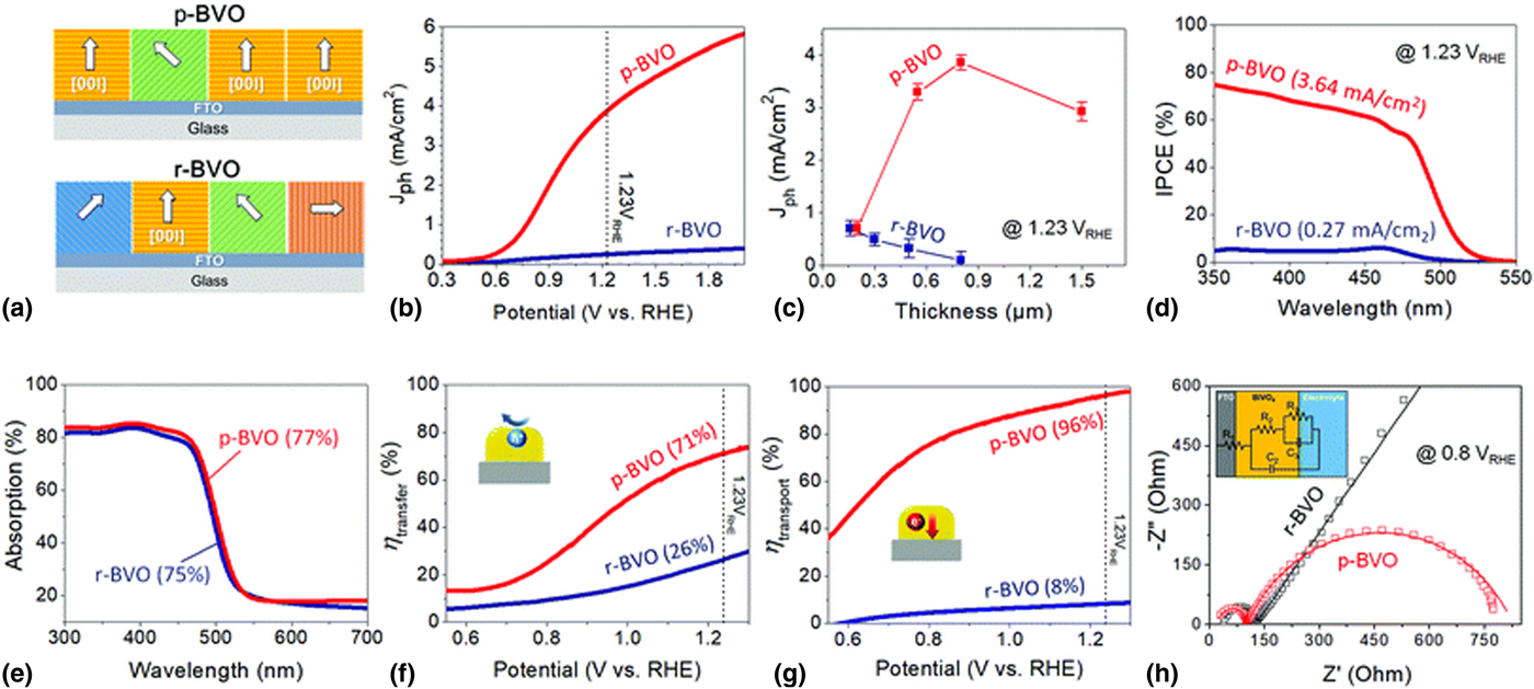
A few studies on facet engineering to enhance the intrinsic properties of BiVO4 photoelectrodes have been reported. Recently, Han et al. reported that pristine BiVO4 photoanodes with [001]-preferred orientation (p-BVO) were deposited by laser ablation method with a KrF excimer laser.[Reference Han, Shin, Kim, Park, Kim, Huang, Lee, Cho and Zheng61] The BiVO4 films composed of rounded-edge columnar grains were ~800 nm thick and about 41% of the grains were the preferred [001] growth orientation (space group: I2/b, a = 5.1935 Å, b = 5.0898 Å, c = 11.6972 Å, 90.3871°). For observation of orientation effects, they synthesized randomly oriented BiVO4 films (r-BVO) by sol–gel drop-casting method [Fig. 2(a)]. As shown in Fig. 4(b), the photocurrent density of p-BVO photoanodes reached 3.9 mA/cm2 (at 1.23 V versus RHE), which was ~16 times higher than that of r-BVO photoanodes (0.25 mA/cm2 at 1.23 V versus RHE). They showed the enhanced charge transport efficiency of p-BVO through the measurements of thickness-dependent J ph,1.23V [Fig. 2(c)]. Unlike r-BVO, the photocurrent density of p-BVO increased with increasing film thickness and remained high even at ~1.5 µm thickness. Improved PEC performance of p-BVO was confirmed by IPCEs [Fig. 2(d)]. The highest IPCE values of p-BVO and r-BVO (at 350 nm) were 74% and 7%. The photocurrent density (J ph) is determined by light absorption expressed in current density (J abs), charge transfer efficiency (η transfer) at the interface between the photoelectode and electrolyte, and charge transport efficiency (η transport).[Reference Dotan, Sivula, Grätzel, Rothschild and Warren62, Reference Chen, Jaramillo, Deutsch, Kleiman-Shwarsctein, Forman, Gaillard, Garland, Takanabe, Heske, Sunkara, McFarland, Domen, Milled and Dinh63]
 $$J_{{\rm ph}} = J_{{\rm abs}} \times \eta _{{\rm transfer}} \times \eta _{{\rm transport}}.$$
(a) Schematic diagram of the different grain orientation between p-BVO and r-BVO. (b) Photocurrent–potential (J–V) curves, (c) thickness-dependent photocurrent densities, (d) incident photon-to-current conversion efficiencies (IPCEs) measurement, (e) light absorption, (f) charge transfer efficiencies, (g) charge transport efficiencies, and (h) the results of electrochemical impedance spectroscopy. Reproduced with permission from Ref. Reference Han, Shin, Kim, Park, Kim, Huang, Lee, Cho and Zheng61. Royal Society of Chemistry, 2018.
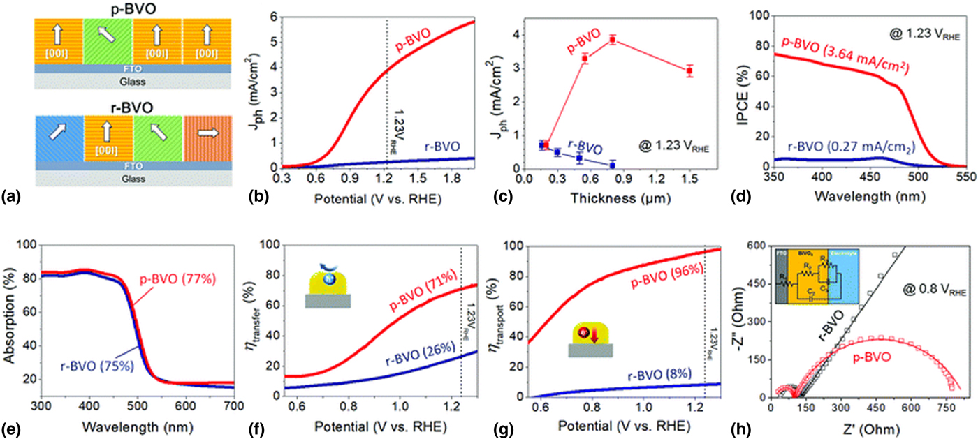
The preferred [001] orientation growth had little effect on light absorption [Fig. 2(e)]. In contrast, the increased η transfer [Fig. 2(f)] and η transport [Fig. 2(g)] contributed to significantly improved PEC performance of p-BVO [Fig. 2(d)]. The results of electrochemical impedance spectroscopy (EIS) measurements [Fig. 2(h)] showed smaller bulk and interface resistances of p-BVO, which was the reason of enhanced η transfer and η transport.
Kim et al. prepared (040)-crystal facet BiVO4 [(040)-BVO] photoanodes (space group: I2/a, a = 5.195 Å, b = 11.701 Å, c = 5.092 Å, β = 90.38°) by hydrothermal method.[Reference Kim, Son, Kang, Kim and Kang64] For investigating the relationship between the (040)-crystal facet and PEC performance, they compared the photoelectrochemical characteristic of (040)-BVO, BiVO4 seed layer, and BiVO4 plate film. The (040)-BVO photoanodes produced the photocurrent density of 0.94 mA/cm2, which was higher than that of BiVO4 seed layer (0.1 mA/cm2) and BiVO4 plate film (0.35 mA/cm2) at 1.23 V versus RHE under AM 1.5G illumination. They explained that (040)-crystal facet induces photogenerated charge flow and enhances charge transfer and charge separation. IPCE and the absorbed photon-to-current conversion efficiency (APCE) of (040)-BVO photoanodes were 37.5% and 42.1% at 1.23 V versus RHE. Based on the equation of IPCE (%) = charge transport efficiency (η trans) × charge separation efficiency (η sep) × charge transfer efficiency at the solid–liquid junction interface (η inter), these IPCE and APCE results were enhanced by using (040)-crystal planes that cause high light absorption and η sep, considering that interfacial charge transfer efficiency is considered when using co-catalysts.[Reference Chen, Dinh and Miller65–Reference Li, Yu, Low, Fang, Xiao and Chen67]
Heterojunction
Due to the broad range absorption of sunlight and enhanced photogenerated electron–hole pair separation with type II band alignment, heterostructures and heterojunctions are reported as promising photoelectrodes.[Reference Kang, Han, Baek, Lee, Song, Bin Kwon, Cho, Jung and Yoon52] Various combinations have been studied for the formation of type II heterojunctions.[Reference Zhao, Wang, Yang, Tang and Yang68–Reference Ju, Wang, Li, Fan, Ai, Zhang and Wang70] Among them, BiVO4/WO3 heterostructure is one of the most attractive combinations.[Reference Hong, Lee, Jang and Lee71]
Since WO3 is stable in aqueous solution under light illumination and can absorb blue light, WO3 has been reported as a good photoanode for PECs. However, theoretical solar-to-hydrogen efficiency is limited up to 4.5% with its wide band gap of 2.7 eV. A synergistic enhancement of the photoactivity can be expected when BiVO4 and WO3 are combined with their merits: good charge transport properties of WO3 and good optical absorption properties of BiVO4.[Reference Hong, Lee, Jang and Lee71] Hong et al. demonstrated BiVO4/WO3 heterojunction electrode for the advanced water oxidation property.[Reference Hong, Lee, Jang and Lee71] Energy band diagram of the heterostructure is depicted in Fig. S3(a). BiVO3 and WO3 construct type II junction; thus, conduction band minimum and valence band maximum of BiVO4 are more negatively located than the conduction band minimum and valence band maximum of WO3. This condition induces the electron injection from BiVO4 to the conduction band of WO3 and hole injection from WO3 to the valence band of BiVO4. Electrons generated in the WO3 layer and electrons migrated to WO3 from the BiVO4 layer are collected onto the F-doped tin oxide layer. This facile transfer of electrons would reduce the recombination rate. Holes, on the other hand, are transferred to the BiVO4 layer from WO3 and migrated to the semiconductor/electrolyte interface to oxidize water. Thus, the heterostructure with type II structure would have enhanced photoactivity and water oxidation property. Photoelectrochemical performance of the BiVO4/WO3 combined structure is measured as Fig. S3(b). Total thicknesses of the films are 3 µm and the portion of BiVO4 is 20%, 40%, 60%, and 80% in composite 1, 2, 3, and 4, respectively. The inset figure of Fig. S3(b) is the magnified view in 0–0.5 V versus Ag/AgCl. The onset potential of WO3 is about 0.25 V versus Ag/AgCl where onsets of composite films are negatively shifted to 0.05 V versus Ag/AgCl by combining with BiVO4 layer. Photocurrent density is also enhanced with composite 1 compared with bare BiVO4 and bare WO3. Photogenerated electrons in BiVO4 are migrated to the WO3 layer with good charge transport characteristics and stimulate the high photoactivity. Thus, fabrication of heterojunction of BiVO4/WO3 is an efficient method to improve the photoelectrochemical performance for water oxidation.
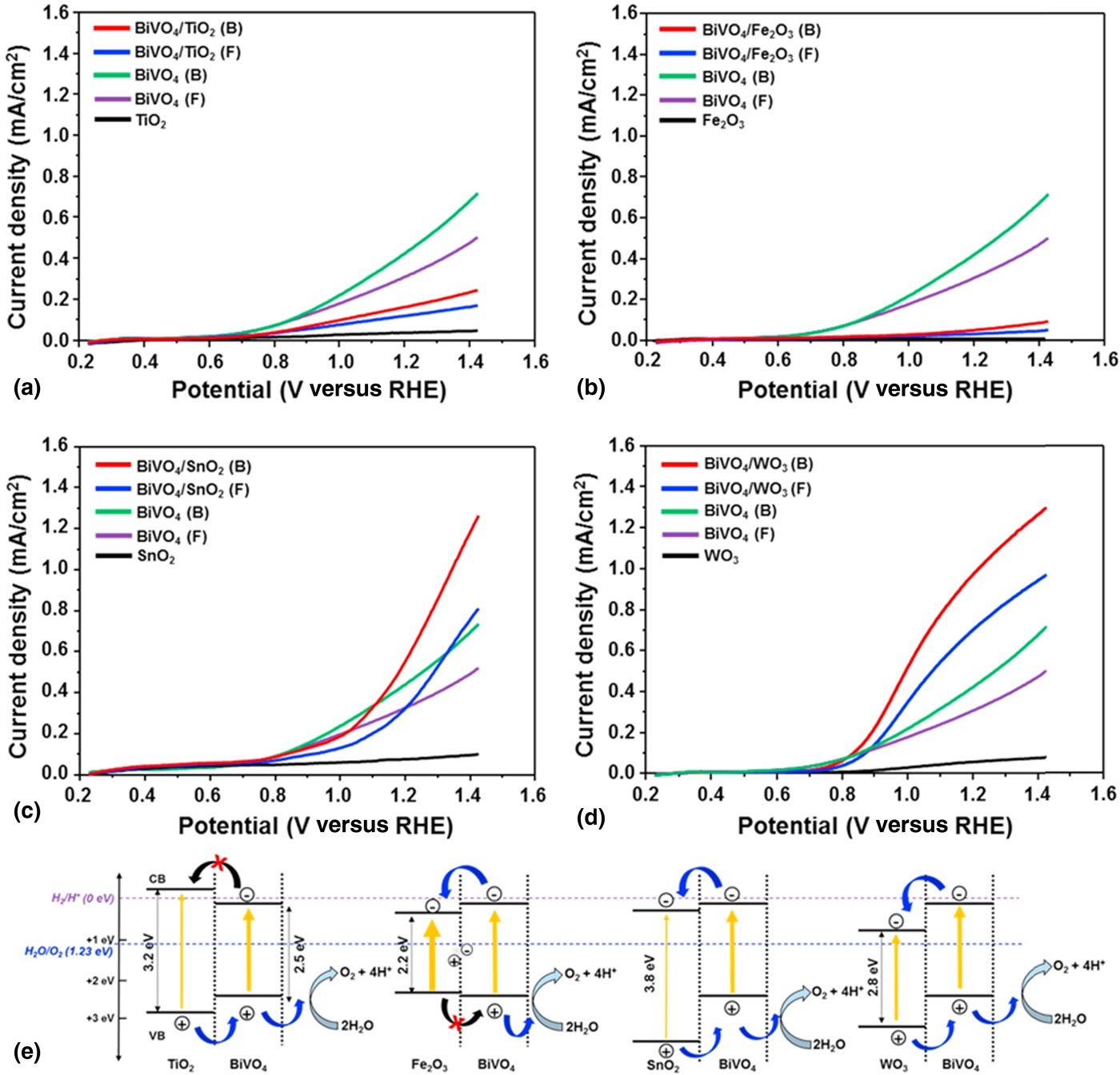
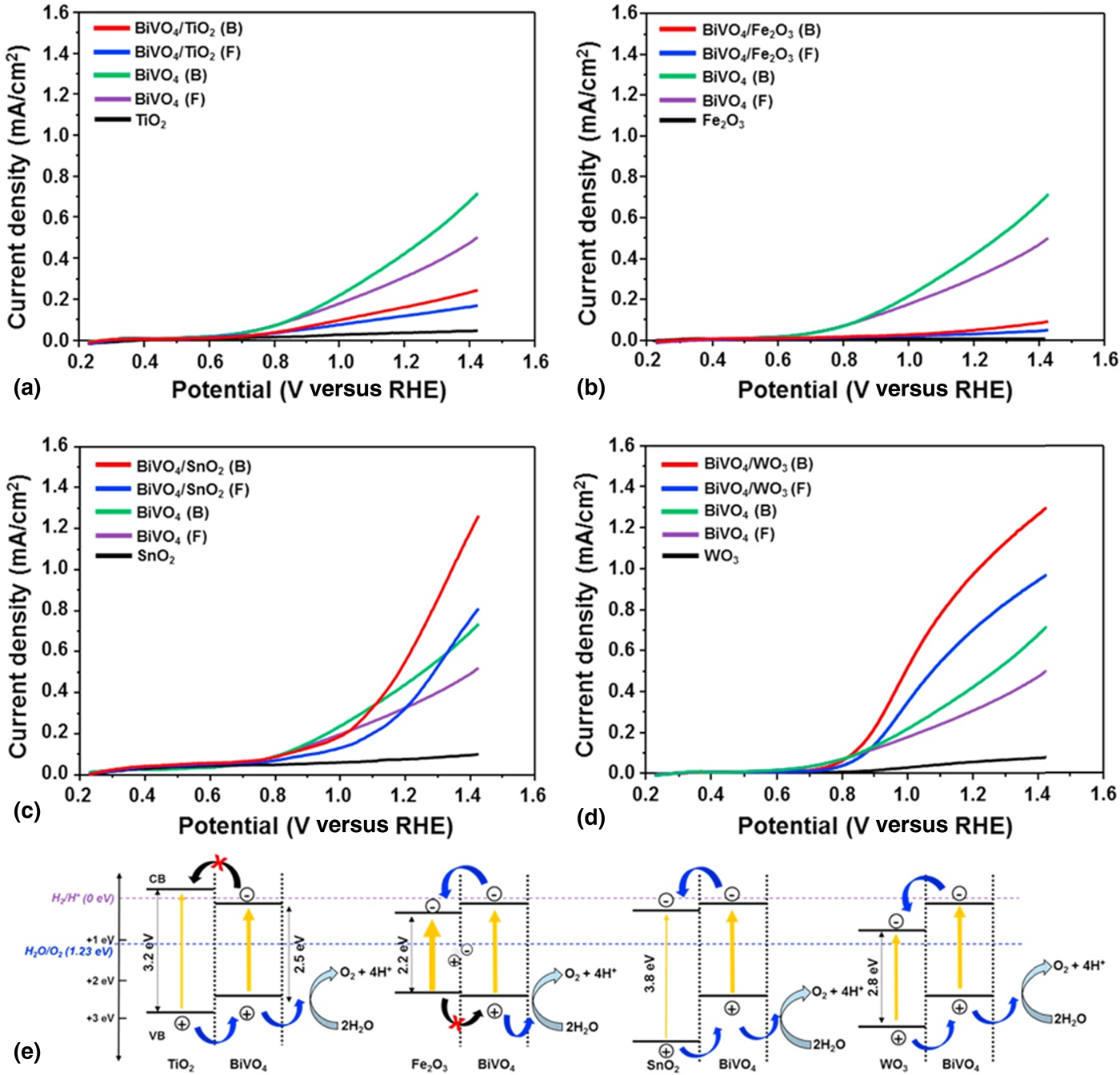
As shown in Fig. 3, various materials including WO3 have been tested to combine with BiVO4 for better water oxidation properties.[Reference Lee, Kim, Sohn, Moon, Park, Lee and Jang72] Linear sweep voltammetry curves of various heterostructures are displayed in Figs. 3(a)–3(d). When BiVO4 is combined with TiO2 and Fe2O3, inferior properties are exhibited (Figs. 3(a) and 3(b)]. The electron affinity of BiVO4 is larger than that of TiO2.[Reference Resasco, Zhang, Kornienko, Becknell, Lee, Guo, Briseno and Yang73] Thus, photogenerated electrons in the BiVO4 layer cannot be transferred to TiO2 as the conduction band minimum of TiO2 is located higher than that of BiVO4. On the other hand, despite the fact that the conduction band minimum of Fe2O3 is lower than that of BiVO4, valence band maximum of Fe2O3 is placed slightly higher than that of BiVO4. Holes generated in the Fe2O3 layer are blocked to be migrated to the BiVO4 layer and these excessive holes recombine with electrons, leading to the lower water oxidizing property of the heterostructure. Combining with SnO2 or WO3 leads to the enhanced water oxidizing performance compared with the bare BiVO4 [Figs. 3(c) and 3(d)]. Both the heterostructures form type II junction, which promotes charge separation and provide conduction pathways. Among these two heterostructures, BiVO4/WO3 shows superior photocurrent density than BiVO4/SnO2 since SnO2 has wide band gap (3.8 eV) where WO3 has smaller band gap (2.6 eV) compared with SnO2.
Photocurrent–potential (J–V) curves of (a) BVO/TiO2, (b) BVO/Fe2O3, (c) BVO/SnO2, and (d) BVO/WO3. (e) Illustrations of the band structures of BVO heterojunction photoanodes. Reproduced with permission from Ref. Reference Lee, Kim, Sohn, Moon, Park, Lee and Jang72. Elsevier, 2016.
Fabricating nanostructured heterojunction photoanode would have much enhanced property.[Reference Lee, Kim, Sohn, Moon, Park, Lee and Jang72, Reference Pihosh, Turkevych, Mawatari, Asai, Hisatomi, Uemura, Tosa, Shimamura, Kubota, Domen and Kitamori74] Porous WO3 nanorods can be deposited with glancing angle deposition method. Pihosh et al. demonstrated a nanostructured BiVO4/WO3 photoanode deposited on the indium tin oxide underlayer with a photocurrent of 3.2 mA/cm2 at 1.23 V versus RHE. With a glancing angle deposition of sputtering, WO3 nanorods are deposited and BiVO4 is deposited on the top of the nanorods.[Reference Pihosh, Turkevych, Mawatari, Asai, Hisatomi, Uemura, Tosa, Shimamura, Kubota, Domen and Kitamori74] The optimum thickness of WO3 and BiVO4 is 2.5 µm and 45 nm, respectively. Figure S4 shows the BiVO4/WO3 heterojunction synthesized by glancing angle deposition (WO3) and pulsed anodic electrodeposition (BiVO4).[Reference Lee, Kim, Sohn, Moon, Park, Lee and Jang72] BiVO4 nanodots are deposited on the entire surface of WO3 nanorods. Figures S4(a) and S4(b) indicate that the deposited BiVO4 nanodots are extremely small. X-ray diffraction data shown in Fig. S4(c) reveal that BiVO4/WO3 heterojunction is fabricated on the F-doped tin oxide substrate. Figures S4(d) and S4(e) designate that the size of the BiVO4 nanodots is about 30 nm. High-resolution images in Figures S4(f) and S4(g) and diffraction patterns of the selected area show that the d-spacing of 0.365 and 0.521 nm correspond to the (110) and (001) planes of monoclinic WO3 nanorods, respectively, and d-spacing of 0.238 nm corresponds to the (220) plane of BiVO4. This nanostructured heterojunction performed the enhancement of photocurrent density at 1.23 V versus RHE. The photocurrent density of nanostructured BiVO4/WO3 is about 4.55 mA/cm2, where the nanostructured WO3 without BiVO4 is about 2.1 mA/cm2. This suggests that the nanostructured heterojunction has all the advantages of BiVO4, WO3, and nanostructure.[Reference Lee, Kim, Sohn, Moon, Park, Lee and Jang72]
Fabricating p–n junction is also an effective way to produce type II band alignment. Chang et al. demonstrated the synergetic enhancement of surface reaction and charge separation by introducing p-type Co3O4 nanodots on n-type BiVO4, forming a p–n junction with an internal electric field to assist the charge separation.[Reference Chang, Wang, Zhang, Zhang, Li and Gong75] As displayed in Fig. S5, photogenerated electrons in BiVO4 are prohibited from transferring to Co3O4, whereas holes on the valence band of BiVO4 can be migrated to that of Co3O4.[Reference Long, Cai, Cai, Zhou, Chai and Wu76] Consequently, the separation of photogenerated electron–hole pairs is substantially improved. In addition, surface reaction can be boosted since Co3O4 lowers the overpotential required for water oxidation.[Reference McAlpin, Surendranath, Dinca, Stich, Stoian, Casey, Nocera, Britt, Dincã, Stich, Stoian, Casey, Nocera and Britt77, Reference Wang and Osterloh78] Photocurrent of Co3O4/BiVO4 p–n junction heterostructure shows 2.71 mA/cm2 at 1.23 V versus RHE for water splitting without a hole scavenger and 6 mA/cm2 at 1.23 V versus RHE with a hole scavenger. Thus, fabricating heterostructure with the materials that can form type II junction is one of the fascinating strategies for superior water oxidation photoelectrode.
Combination with plasmonic nanoparticles
Plasmonic metal NPs have been actively studied for solar water splitting due to their ability to overcome many limitations of photoanodes. Especially, gold (Au) and silver (Ag) NPs are mainly used for solar water splitting because of their chemical stability, Schottky junction formation, and localized surface plasmon resonance (LSPR) in the visible spectral region. The formation of Schottky junction improves charge transfer, modifies the electronic band structure, and promotes charge separation.[Reference Li, Cushing, Zheng, Meng, Chu and Wu79] LSPR also has several advantages in improving solar water splitting.[Reference Lee, Moon, Park, Sohn, Kang, Lee, Choi and Jang80–Reference Abdi, Dabirian, Dam and van de Krol84] First, the plasmon-resonant energy transfer (PRET) effect can produce field-enhanced electron–hole pair near the semiconductor surface. Second, plasmon-induced direct electron transfer (DET) contributes to the creation of additional charge carriers through injecting the hot electrons generated by surface plasmons into the conduction band of the semiconductor. Third, resonant photon scattering of metal NPs greatly increases the average photon path length. Au and Ag NPs can reduce the charge recombination rate because of strong surface plasmon resonance and confinement of the light near their surface.[Reference Zhang, Herrmann and Baumberg81–Reference Valenti and Smith83, Reference Halas, Lal, Chang, Link and Nordlander85–Reference Hu, Diao, Xu and Wu88]
There are several studies on BiVO4 with geometrically controlled plasmonic Au or Ag NPs. Zhang et. al investigated BiVO4 films with Au NPs size-dependent plasmonic effect.[Reference Zhang, Herrmann and Baumberg81] They prepared photoanodes by drop-casting Au NPs with the diameters of 10, 20, 30, 40, 60, and 80 nm onto the BiVO4 films. All of the BiVO4 photoanodes with Au NPs showed higher photocurrent densities than the BiVO4 photoanodes without Au NPs, and 20 and 30 nm Au NPs on BiVO4 photoanodes obtained highest photocurrent densities. In order to understand the PRET effect with different sizes of Au NPs, they simulated the electric field distribution based on finite-different time-domain (FDTD) method. The simulation showed that with increasing the size of Au NP, the volume of electric field enhancement also increased. The photogenerated holes with enhanced electric field are able to diffuse the BiVO4 surface. It means that the photogenerated charge carrier can be separated in the space charge layer. They also observed the enhancement factor that varied with incident light wavelength. The electric field enhancement reached a maximum value at around 580 nm for all of the Au NPs. This enhanced light absorption and localized light absorption on the BiVO4 surface can help the readily separated charge carrier generation in the space charge layer. But for the experiment, Au NPs with larger diameter than 40 nm reduced the PRET effect because of the red shift of the plasmonic absorption resonance. They confirmed that, unlike the PRET effect, the effect of scattering and hot electron injection were weak for the BiVO4 photoanodes with Au NPs. They also performed the angle-dependent PRET effect, and they observed strong PRET effect with larger off-normal irradiation angles.
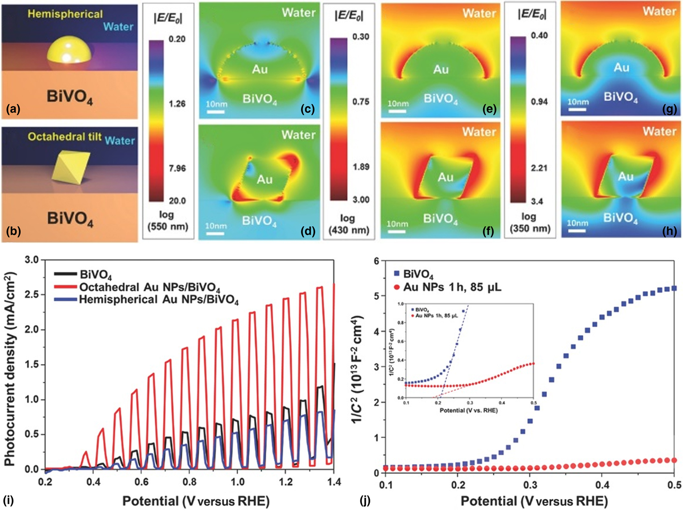
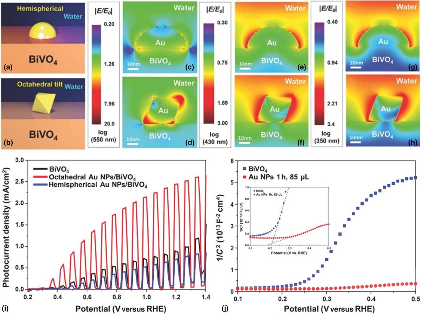
Recently, BiVO4 photoanodes with shape-controlled Au NPs also have been studied. Hemispherical and octahedral Au NPs have been utilized to observe the shape-dependent plasmonic effect.[Reference Lee, Moon, Park, Sohn, Kang, Lee, Choi and Jang80] BiVO4 films were deposited by pulsed anodic electrodeposition method with post-annealing process for crystalline monoclinic phase. Octahedral Au NPs were synthesized by seed-mediated growth method, and then they attached them on prepared BiVO4. Hemisphere Au-deposited BiVO4 was deposited by electron beam evaporator. In order to observe the Au NP shape-dependent field enhancement, they performed FDTD simulation [Figs. 4(a)–4(h)]. BiVO4 films with octahedral NPs showed higher intensified LSPR electric fields (LSPR-EFs) than the hemisphere Au NPs due to their well-defined edges and sharp vertices.[Reference Valenti and Smith83, Reference Wang, Ye, Iocozzia, Lin and Lin89–Reference Kundu91] The sharp vertices of plasmonic Au NPs reduce the restoring force of electron oscillation, which can enhance the charge separation in the semiconductor.[Reference Moon, Lee, Sohn, Andoshe, Kim, Hong and Jang92, Reference Liu, Yan, Kang, Li, Shen, Sun, Wang and Zhang93] The photocurrent density of BiVO4 photoanodes with octahedral Au NPs reached 2.4 mA/cm2 at the 1.23 V versus RHE, which was three times higher than that of bare BiVO4 photoanodes [Fig. 4(i)]. This is due to their high absorption, enhanced charge generation, and improved charge separation by DET and PRET, which are LSPR-induced effects.
Finite-difference time-domain (FDTD) configurations on BVO. (a) Hemispherical Au NP and (b) octahedra Au NP. Field enhancement for (c) hemispherical Au NP and (d) octahedral Au NP under 550 nm photons. Field enhancement for (e) hemispherical Au NP and (f) octahedral Au NP under 430 nm photons. Field enhancement for (g) hemispherical Au NP and (h) octahedral Au NP under 350 nm photons. (i) Photocurrent–potential (J–V) curves and (j) Mott–Schottky plot. Reproduced with permission from Ref. Reference Lee, Moon, Park, Sohn, Kang, Lee, Choi and Jang80. WILEY-VCH Verlag GmbH & Co. KgaA, Weinheim, 2017.
Jeong et al. studied about plasmonic Ag NPs with BiVO4 photoanodes.[Reference Jeong, Shin, Jo, Kim, Kim, Lee, Lee, Song, Moon, Seo, An, Lee, Song, Kim, Yoon and Lee94] Fully solution-deposited Ag-impregnated nanocomposite BiVO4 (Ag-BVO) photoanodes were studied for solar water splitting. The simulation showed that impregnated Ag NPs in BiVO4 maximized the use of the LSPR-induced enhancement effect. The photocurrent density of Ag-BVO photoanodes was 3.3 times higher than that of pristine BiVO4 photoanode at 0.4 V versus RHE. They explained it by the mechanism of LSPR-induced enhancement. When they illuminated the visible light and ultraviolet light, both of BiVO4 and Ag NPs absorbed the light and the Ag NPs generated the localized electric field by LSPR. The steep increase and the improved saturated current density are attributed to the carrier concentration increase by the charge carrier generation. In order to characterize the carrier excitation in Ag-BVO, they measured photoluminescence (PL). The results showed that the PL intensities increased with increasing concentration of Ag NPs. It is because the intensities of PL are proportional to the amount of carrier recombination. Therefore, the results of PL imply that an increase of carrier concentration is the result of the LSPR-induced effects. They also analyzed the EIS for observing the improved charge carrier separation mechanisms induced by Schottky junction formation.[Reference Linic, Christopher and Ingram82, Reference Li, Zhou, Hao and Li95–Reference Thomann, Pinaud, Chen, Clemens, Jaramillo and Brongersma101]
Co-catalyst loading
The biggest limitations of BiVO4 are poor surface catalytic reaction for water oxidation and slow kinetics for oxygen evolution.[Reference Park, McDonald and Choi23, Reference Abdi and van de Krol32, Reference McDonald and Choi102] Thus, various types of electrocatalysts, such as cobalt phosphate (Co-Pi), NiOOH, FeOOH, and CoOx are commonly deposited on the top of the BiVO4 electrode to improve the charge transfer efficiency.[Reference Kim and Choi50, Reference Kang, Han, Baek, Lee, Song, Bin Kwon, Cho, Jung and Yoon52] The most commonly used catalyst to improve water oxidation kinetics is Co-Pi catalyst developed by Kanan and Nocera.[Reference Kanan and Nocera18] Accumulation of holes in the surface of the BiVO4 results in the recombination of electrons and holes. Co-Pi blocks the accumulation of holes in the interface since Co-Pi-catalyzed surface has faster water oxidizing kinetics and lower overpotential is required. Co-Pi has been reported to improve the performance of Fe2O3,[Reference Zhong, Cornuz, Sivula, Grätzel and Gamelin97, Reference Zhong, Sun, Inumaru and Gamelin103, Reference Zhong and Gamelin104] WO3,[Reference Seabold and Choi98] and other photoanode materials under neutral pH conditions.[Reference Steinmiller and Choi105–Reference Young, Costi, Paydavosi, Nocera and Bulović107] Certainly, Co-Pi is also effective for the performance of BiVO4 photoelectrode.[Reference Abdi and van de Krol32] For photoelectrochemical water oxidation, the thickness of the Co-Pi catalyst layer is sensitive; thus, fine tuning of the thickness is indeed needed to optimize the performance.[Reference Luo, Yang, Li, Zhang, Liu, Zhao, Wang, Yan, Yu and Zou108, Reference Jeon, Choi and Park109]
Abdi and van de Krol reported 1.7 mA/cm2 at 1.23 V versus RHE without a hole scavenger for Co-Pi-catalyzed BiVO4 photoanodes with a thickness of 100 nm prepared by spray pyrolysis.[Reference Abdi and van de Krol32] As shown in Fig. S6(a), the photocurrent density of bare BiVO4 is 0.6 mA/cm2, whereas Co-Pi-catalyzed BiVO4 has much enhanced value. Photocurrent transient measurements are depicted in Fig. S6(b). When the sample absorbs light, photogenerated holes travel to the electrode surface and accumulate because of the poor oxygen evolution reaction kinetics.[Reference Sanchez, Sieber and Somorjai110] Thus, a sharp anodic current spike is appeared and the current density decays as the accumulation process reaches the equilibrium.[Reference Le Formal, Tétreault, Cornuz, Moehl, Grätzel and Sivula111] When the light is switched off, the accumulated holes recombine with electrons in the conduction band, causing the cathodic response of the black line in Fig. S6(b). With the Co-Pi catalyst layer, hole injection rate of water is enhanced, leading to the low electron–hole recombination. Consequently, photocurrent for water oxidation without a hole scavenger is improved to the level of photocurrent for H2O2 oxidation, indicating that oxygen evolution kinetics are improved. Figure S6(c) shows the photocurrent density as a function of the thickness of Co-Pi on BiVO4 photoelectrode. Co-Pi thickness of 30 nm has the highest photocurrent density compared with other thicknesses. Thus, the optimum thickness of Co-Pi is about 30 nm. This is because the Co-Pi layer is not wholly covering the BiVO4 when the thickness is thinner than 30 nm, while hole transport through the Co-Pi layer may become worse for thicker films.[Reference Abdi and van de Krol32]
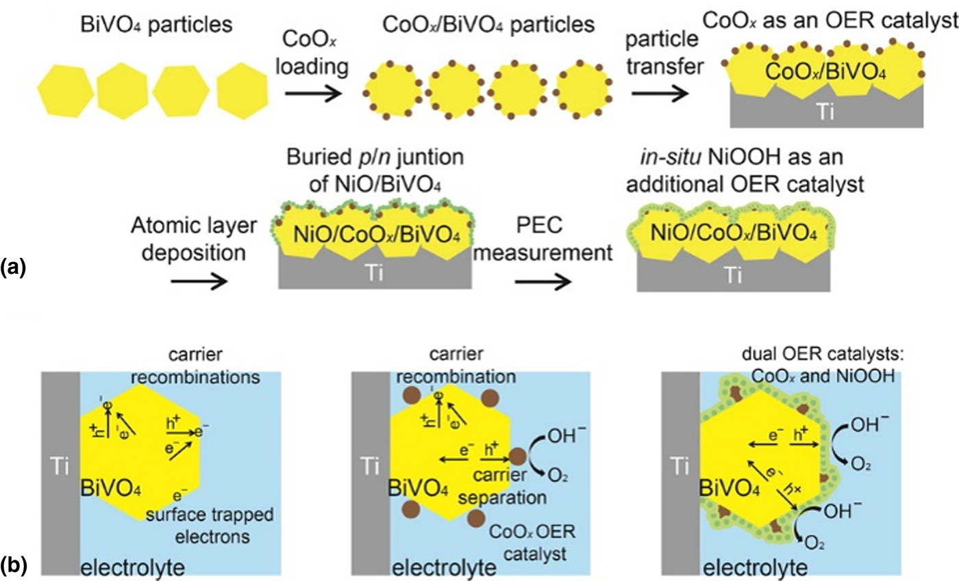
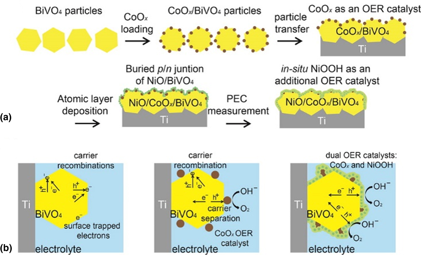
Loading NiO on the surface of BiVO4 is one of the feasible approaches to enhance water-splitting performance. Since NiO is a p-type oxide, a buried p–n junction can be easily created at the photoanode surface with NiO surface layer. The photogenerated holes will be extracted from BiVO4 photoanode and stored in the surface p-type NiO with a prolonged life time. In addition, p-type NiO would turn into hydroxyl-ion permeable NiOOH on the photoanode surface during water oxidation process. Zhong et al. demonstrated dual catalyzed BiVO4 NPs with CoOx and NiO for photoelectrochemical water oxidation.[Reference Zhong, Hisatomi, Kuang, Zhao, Liu, Iwase, Jia, Nishiyama, Minegishi, Nakabayashi, Shibata, Niishiro, Katayama, Shibano, Katayama, Kudo, Yamada and Domen112] The NiOOH layer is formed at the surface as shown in Fig. 5. The optimal thickness of NiO layer is 6 nm and NiO/CoOx/BiVO4 photoanode reaches 3.5 mA/cm2 at 1.23 V versus RHE, which is a twofold increased value compared with that of the CoOx/BiVO4 photoanode.[Reference Zhong, Hisatomi, Kuang, Zhao, Liu, Iwase, Jia, Nishiyama, Minegishi, Nakabayashi, Shibata, Niishiro, Katayama, Shibano, Katayama, Kudo, Yamada and Domen112] Kim and Choi assembled thin NiOOH and FeOOH layers on the nanoporous BiVO4 surface.[Reference Kim and Choi50] Photocurrent of the NiOOH/BiVO4 and FeOOH/BiVO4 photoanodes was significantly higher than the bare BiVO4 photoanode. Thus, depositing NiO on the surface which will naturally turn into NiOOH can be also applied to other semiconducting photoelectrode toward highly efficient solar fuel generation.
(a) Fabrication process of the NiOOH/NiO/CoOx/BVO/Ti photoanodes and (b) schematic diagram of proposed recombination/separation process. Reproduced with permission from Ref. Reference Zhong, Hisatomi, Kuang, Zhao, Liu, Iwase, Jia, Nishiyama, Minegishi, Nakabayashi, Shibata, Niishiro, Katayama, Shibano, Katayama, Kudo, Yamada and Domen112. American Chemical Society Publications, 2015.
Control of interfacial band bending with ferroelectrics
Ferroelectric materials have ferroelectric self-polarization field and high built-in potential that can improve the drift and separation of photogenerated carriers.[Reference Song, Kim, Lee, Cho, Cha, Jeong, An, Kim, Jung, Park, Jung, Kim, Jo, Bu, Jang and Lee10, Reference Xie, Guo, Yang, Wang, Liu and Li113] Recently, BiFeO3 (BFO) perovskite ferroelectric material is actively studied for enhancing the solar water splitting. Because it possesses high Curie temperature (T c = 1000 K), suitable bandgap energy (~2.1 eV) is required to absorb the visible light, intrinsic polarization field, and chemical stability.[Reference Xie, Guo, Yang, Wang, Liu and Li113–Reference Zhang, Yang, Liang, Zheng, Wang, Gao, Yuan, Zhang, Li, Luo and Zheng116] Until recently, there have been a few papers that have greatly enhanced the results of BFO photoanodes-based PEC because of their high dielectric constant, low visible light absorbance, and their insulating nature.
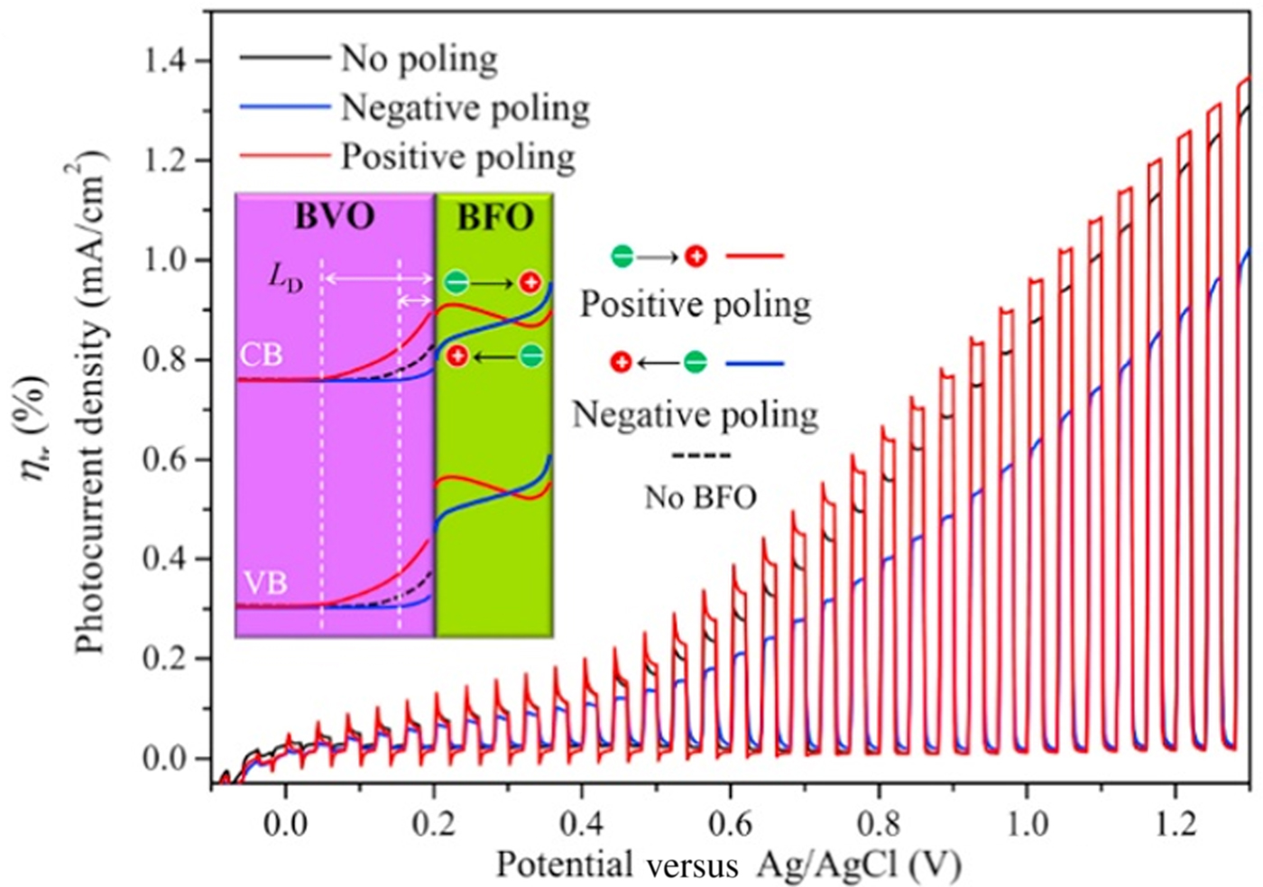
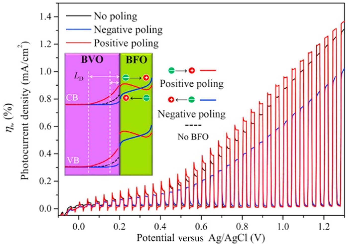
Xie et al. reported that the BFO passivated BiVO4 (BVO/BFO) photoanodes showed enhanced photoelectrochemical properties.[Reference Xie, Guo, Yang, Wang, Liu and Li113] They synthesized BiVO4 thin films by dipping method with post-annealing process. After the preparation of the BiVO4 films, they fabricated BVO/BFO thin films by chemical solution deposition method. The photocurrent density of BVO/BFO photoanode was 0.63 mA/cm2 at 0.6 V versus RHE, which is 4.4 and 1.24 times higher than that of bare BVO and BVO/Co-Pi photoanodes. The onset voltage of the BVO/BFO photoanode was 0.03 V versus RHE, which is ~0.40 and ~0.22 V lower than that of the BVO and BVO/Co-Pi photoanodes. It means that the BFO passivation layer accelerates the OER kinetics in photoanode. In order to confirm the ferroelectric polarization effect, they measured PEC performance after poling the BVO/BFO photoanode (Fig. 6). The photocurrent density of the BVO/BFO with positive poling increased by 19%. In contrast, the photocurrent density with negative poling decreased to be ~75.6%, which means that the band bending is downward at the surface and the charge separation efficiency is limited. These results imply the exist of the self-polarization direction of the BFO layer. They also showed greatly enhanced APCE value of 21.2% at the wavelength of 360 nm compared with 10.0% and 15% of bare BVO and BVO/Co-Pi photoanodes. It means that the BFO passivation layer can suppress the charge recombination. The charge transfer and separation efficiency were also enhanced and the long-term stability was better than BVO/Co-Pi photoanode. They explained that the self-polarization of BFO and the type II heterojunction formed by contacting the BVO with BFO can result in the suppressed charge recombination and improved charge transfer/surface OER reaction. The self-polarization in BFO can be caused by strain, oxygen vacancies, and so on, and the effect of self-polarization becomes more important with decreasing the BFO thickness.[Reference Dong, Guo, Guo, Li, Liu and Joel117] This means that the thin passivation BFO layer can play a critical role in the formation of a high self-polarization.
Chopped photocurrent–potential (J–V) curves and schematic mechanism of the BVO/BFO photoanode. Reproduced with permission from Ref. Reference Xie, Guo, Yang, Wang, Liu and Li113. Elsevier, 2017.
Summary and outlook
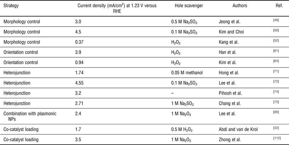
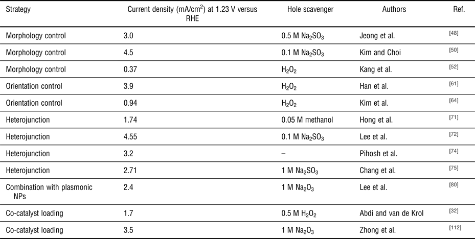
In summary, we have reviewed the strategies to enhance the water oxidizing properties of BiVO4 for a photoanode in a PEC. Many attempts have been made to improve the performance of BiVO4 such as fabricating nanostructured BiVO4, controlling reacting facet, stacking with other materials, utilizing plasmonic effects, loading co-catalyst, and controlling the interfacial band bending with ferroelectrics as shown in Table I. However, the practical conversion efficiency attained with the BiVO4-based photoelectrode is still below what expected owing to some drawbacks such as low electron–hole separation yield and slow kinetics for water oxidation. Thus, theoretical and experimental studies to further enhance the property of BiVO4 are highly desired.
Review on the strategies and photoelectrochemical performance of references.
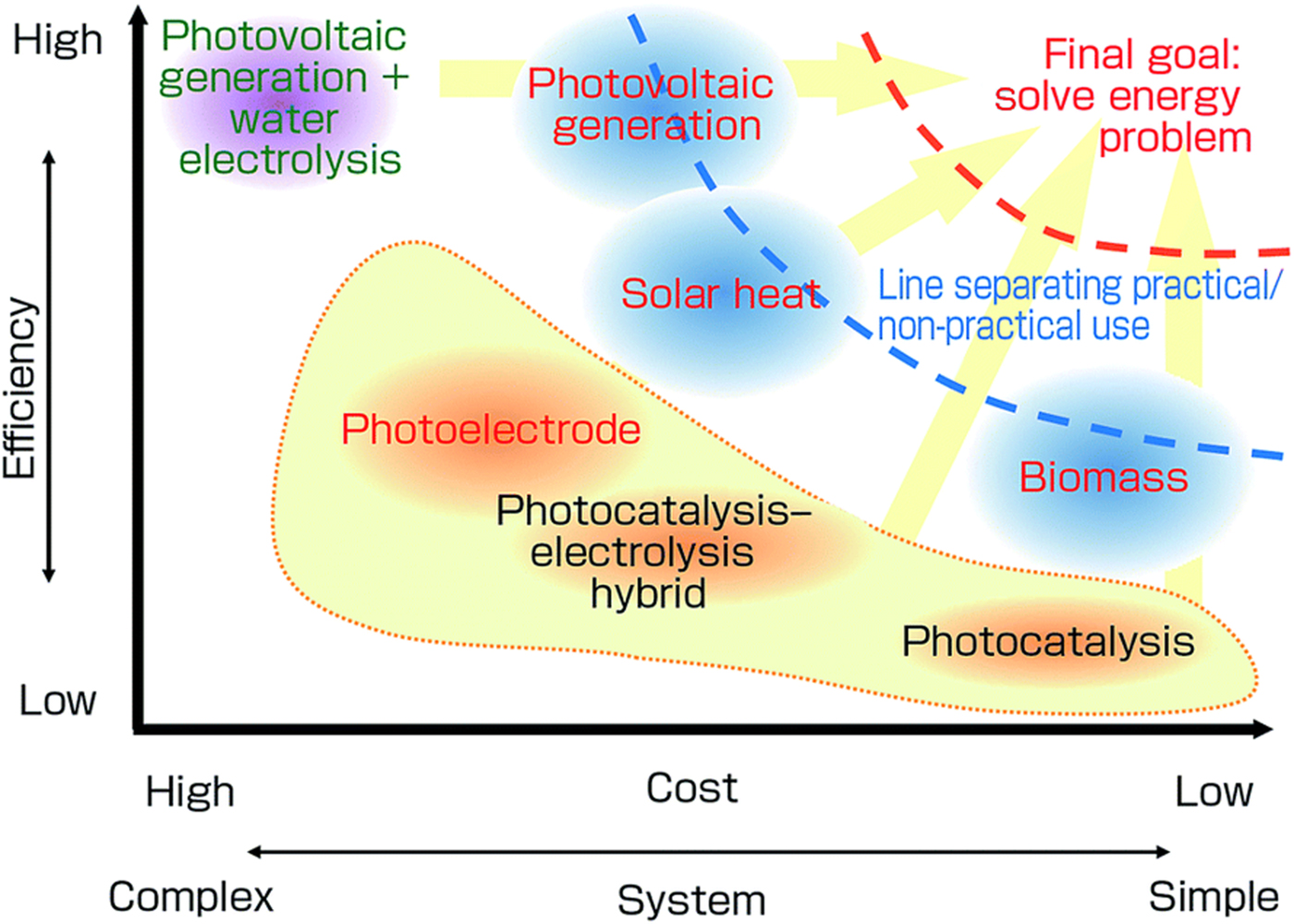
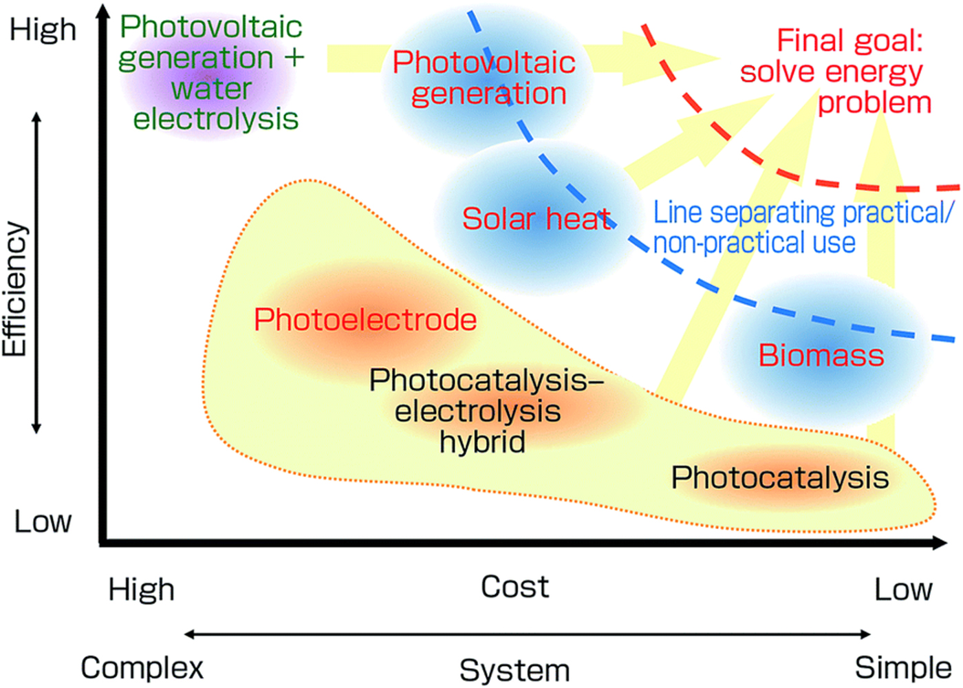
The US Department of Energy has set the technical target of the solar-to-hydrogen energy conversion efficiency of the photoelectrode system as 20% for 2020.[118] Sayama and Miseki summarized the cost and efficiency of various solar energy conversion systems in the schematic as shown in Fig. 7.[Reference Sayama and Miseki119, Reference Hisatomi and Domen120] To date, photovoltaic-assisted electrolysis system shows superior efficiency than photoelectrode water-splitting system. However, this system is too expensive to be cost-competitive. Therefore, the development of photoelectrode solar water-splitting system is required. The strategies, discussion, and insights contained in this article provide a good understanding for current state and development of BiVO4. It is expected that, by combining one or several strategies, the solar-to-hydrogen conversion efficiency of BiVO4-based photoelectrode can be stimulated to a suitable level for practical solar water splitting.
Technologic map showing various approaches to solar energy conversion. Reproduced with permission from Ref. Reference Hisatomi and Domen120. Royal Society of Chemistry, 2017.
Supplementary material
The supplementary material for this article can be found at https://doi.org/10.1557/mrc.2018.106
Acknowledgments
This work was financially supported by the Future Material Discovery Program (NRF-2016M3D1A1027666) and the Basic Science Research Program (NRF-2017R1A2B3009135) through the National Research Foundation of Korea.