Brief overview of probe data storage
A “probe data storage device” can be defined as a storage device where a mobile “probe” serves as the reader/writer of a storage device. Edison’s phonography, CDs, DVDs, and hard disk drives (HDDs) are good examples of “probe data storage devices”—they all incorporate a stylus, optical pickup or head as mobile probes, and their media vary from polymers to magnetic coatings.Reference Hong, Park, Kalinin and Gruverman1,2
HDDs have a separate reader and writer,Reference Wang and Taratorin3 where the writer typically is an inductive coil, while the reader has led the exponential increase in the density of stored information, starting from the inductive coil through magnetoresistance (MR) heads to giant magnetoresistance, and more recently, to tunneling magnetoresistance heads. Media today have evolved from longitudinal magnetic recording media to perpendicular magnetic recording media due to the superparamagnetic limit of the media, at which point the magnetic moment fluctuates randomly by thermal energy.Reference Khizroev and Litvinov4
In the early 2000s, the need for smaller form factor was driving the storage device industry toward mobile high-density devices. However, these devices were facing big challenges for further miniaturization while maintaining high information density. This led to a paradigm shift from traditional mechanical assembly to silicon processing, similar to microelectromechanical systems (MEMS) design for further miniaturization of probe data-storage devices. The first step was provided by IBM researchers, when they invented the scanning probe microscope in 1981.Reference Binnig, Quate and Gerber5,6
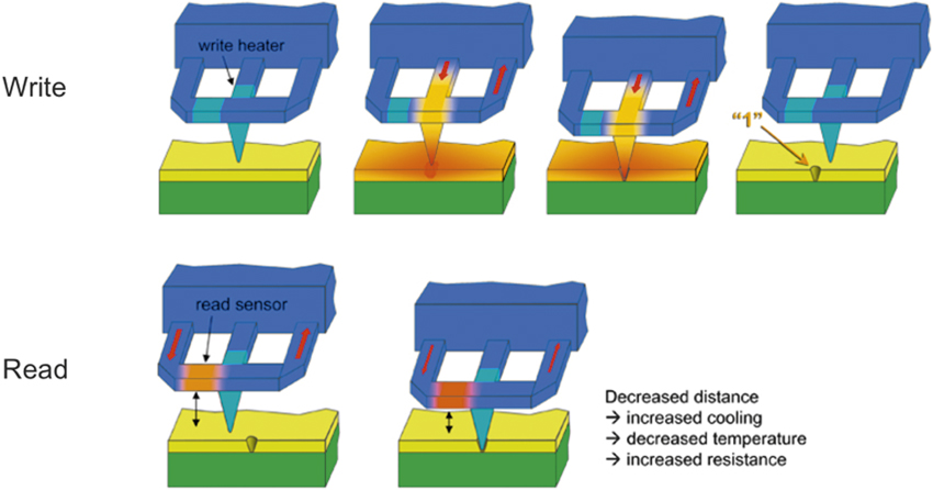
IBM further developed the idea of using the probe for simple measurement and imaging to probe storage devices; they realized that the same probe technology could be applied to storage devices if combined with MEMS and HDD technology.Reference Lutwyche, Andreoli, Binnig, Brugger, Drechsler, Häberle, Rohrer, Rothuizen, Vettiger, Yaralioglu and Quate7 The working principle was similar to the old phonograph in the sense that data written in the form of nano- or atomic-scale grooves indented by a heated tip. The doped silicon probe acted as a heater and indenter when it heats itself and hits the media with a mechanical force to form an indentation mark (Figure 1).Reference Vettiger, Cross, Despont, Drechsler, Dürig, Gotsmann, Häberle, Lantz, Rothuizen, Stutz and Binnig8 The silicon heater also acts as a reader when it scans over the indentation by using the temperature-dependent resistance of the doped silicon probe. The heat-dissipation rate changes depending on the air gap between the cantilever and the media surface, which, in turn, determines the temperature and accordingly the resistance of the probe. Thus, it was named thermomechanical probe storage.Reference Vettiger, Cross, Despont, Drechsler, Dürig, Gotsmann, Häberle, Lantz, Rothuizen, Stutz and Binnig8
Schematic diagrams of (upper) thermomechanical writing and (lower) reading processes. (Upper) Writing involves heating of the cantilever by a current flowing between two terminals (center and right legs) of the cantilever and applying a force in the normal direction to the film surface. (Lower) Reading involves flowing a small current through the reading element between two terminals (left and right legs), where resistance is sensitive to the gap between the reading element on the cantilever and the sample surface. This distance will decrease when the tip is inside the pit and will lead to an increase in the resistance of the reading element.Reference Vettiger, Cross, Despont, Drechsler, Dürig, Gotsmann, Häberle, Lantz, Rothuizen, Stutz and Binnig8

Thermomechanical data storage (Millipede)
IBM developed the “Millipede,” a thermomechanical probe storage device (Figure 2),Reference Gruener9 which is composed of thousands of atomic force microscope (AFM) tips that run in parallel to write and read data in the form of tiny depressions in a polymer media—data densities were shown to exceed 1 Tbit/in2 (1.55 Pbit/m2) in 2004. IBM’s most recent array design consists of an array of 64 × 64 cantilevers on a 100-µm pitch, where the 6.4 × 6.4 mm2 array is fabricated on a 10 × 10 mm2 silicon chip using the “transfer and join” technology, allowing the direct interconnection of the cantilevers with complementary metal oxide semiconductor (CMOS) electronics used to control the operation of the cantilevers.Reference Eleftheriou, Antonakopoulos, Binnig, Cherubini, Despont, Dholakia, Duerig, Lantz, Pozidis, Rothuizen and Vettiger10 The cantilevers used in the array have a three-terminal design, with separate heaters for reading and writing, and a capacitive platform for electrostatic actuation of the cantilevers in the z-direction. The apex of each tip has a radius on the scale of a few nanometers allowing data to be written at densities greater than 1 Tbit/in2 (1.55 Pbit/m2).Reference Eleftheriou, Antonakopoulos, Binnig, Cherubini, Despont, Dholakia, Duerig, Lantz, Pozidis, Rothuizen and Vettiger10
Photograph of the Millipede prototype.Reference Gruener9

Thermomechanical writing is performed by locally heating the polymer media using the tip of a cantilever while applying a force to create a nanoscale indentation in the polymer film. Readback of the data is performed using a thermomechanical sensing technique, where a second resistive heater integrated into the cantilever is heated to a temperature of approximately 200°C while the polymer medium is scanned under the tip. The principle of thermal sensing is that the rate of cooling of the heater increases as the distance between the tip and the polymer medium is reduced. When the tip moves into an indentation, the distance between the heater and substrate is reduced, resulting in an increase in cooling, which leads to an increase in resistance of the heater.Reference Lutwyche, Despont, Drechsler, Durig, Haberle, Rothuizen, Stutz, Widmer, Binnig and Vettiger11 Using a small-scale prototype, IBM has demonstrated the storage and retrieval of user data using multiple cantilevers at storage densities up to 517 Gb/in2 (801 Tbit/m2).Reference Pozidis, Haeberle, Wiesmann, Drechsler, Despont, Albrecht and Eleftherioum12
Inspired and encouraged by the IBM millipede, there have been efforts around the world to implement a faster and more reliable read/write mechanism into the probe storage scheme, including companies such as HP,13 Seagate,Reference Zhao, Johns and Forrester14,Reference Forrester, Ahner, Bedillion, Bedoya, Bolten, Chang, de Gersem, Hu, Johns, Nassirou, Palmer, Roelofs, Siegert, Tamaru, Vaithyanathan, Zavaliche, Zhao and Zhao15 Canon,Reference Yano, Kyogaku, Kuroda, Shimada, Shido, Matsuda, Takimoto, Albrecht, Eguchi and Nakagiri16 Pioneer,Reference Takahashi, Ono, Cho and Esashi17 LG,Reference Lee, Nam, Kim, Jin, Cho and Bu18,Reference Setter, Damjanovic, Eng, Fox, Gevorgian, Hong, Kohlstedt, Kingon, Park, Stephenson, Stolitchnov, Tagantsev, Taylor, Yamada and Streiffer19 Intel,Reference Kim, Adams, Tran, Ma and Rao20 and Samsung.Reference Hong, Park, Kalinin and Gruverman1,Reference Park, Jung, Min, Kim, Hong and Shin21 Seagate, Samsung, Pioneer, and Intel adopted ferroelectric media and used resistive probes,Reference Park, Jung, Min, Kim, Hong and Shin21,Reference Ko, Ryu, Park, Park, Kim, Jung, Min, Kim, Shin and Hong22 charge gradient probes,Reference Hong, Tong, Park, Hiranaga, Cho and Roelofs23 or scanning nonlinear dielectric microscope (SNDM) probesReference Cho24 as the writer and reader where simple voltage application through the tip induces local polarization switching beneath the tip. The written domain was also read using either resistive probes, charge gradient probes, or SNDM probes.
Ferroelectric probe data storage based on scanning nonlinear dielectric microscopy
Ferroelectrics can hold memory bit information in the form of the spontaneous polarization direction of individual domains. Spontaneous polarization is electric polarization existing without electric field application, and its direction can be switched by the application of an electric field. Ferroelectric recording is thus a data rewritable recording method. The major advantage of using ferroelectrics as a recording medium is its thin domain walls. The domain walls of typical ferroelectric materials are on the order of a few crystal lattice parameters,Reference Merz25,Reference Matsuura, Cho and Ramesh26 which is favorable for high-density data storage due to the ability to allow abrupt changes in polarization. The basic idea of applying ferroelectrics to a recording system has been suggested for a long time.Reference Jona and Shirane27 However, different from magnetic recording, in ferroelectric data storage, the remanent polarization does not produce an external field even after the recording medium has been polarized, because the remanent polarization is neutralized by the free charge. Therefore, in ferroelectric data storage, the reproduction of stored information is somewhat difficult.
In 1994, Cho et al. developed the SNDM for observations of ferroelectric polarization distributions to address this problem.Reference Cho, Kirihara and Saeki28,Reference Cho, Kazuta and Matsuura29 The resolution of the SNDM is in the subnanometer range for ferroelectric domain measurement and at the atomic scale for surface observations of semiconductors.Reference Cho and Hawkes30–Reference Cho and Hirose32 This is much higher than the piezoresponse force microscopy (PFM) method typically used for observing polarization distributions.Reference Guthner and Dransfeld33–Reference Paruch, Tybell and Triscone37 Moreover, the SNDM technique is a purely electrical method, allowing domain information to be read at much higher speeds than by PFM imaging, the read speed of which is limited by the mechanical resonant frequency of the AFM cantilever. Therefore, ferroelectric high-density data storage based on SNDM has been intensively studied for 20 years.Reference Tanaka, Kurihashi, Uda, Daimon, Odagawa, Hirose, Hiranaga and Cho38
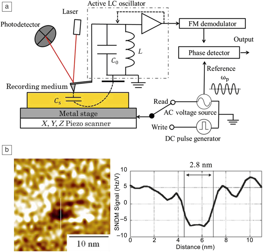
Figure 3a shows a schematic diagram of a ferroelectric data-storage system based on SNDM. The SNDM probe is composed of a conductive cantilever tip and an oscillator. Polarization distinction is performed by detecting the small variation in resonance frequency caused by the variation in the capacitance due to the nonlinear dielectric response induced by the alternating voltage applied to the ferroelectric recording medium, since the sign of the capacitance variation depends on the polarization direction.
(a) Schematic diagram of ferroelectric data-storage system based on scanning nonlinear dielectric microscopy (SNDM). (b) Smallest artificial nanodomain single dot with a size of 2.8 nm in diameter formed and observed by using SNDM. (Left) SNDM image and (right) profile taken along the white line in the left image.Reference Tanaka, Kurihashi, Uda, Daimon, Odagawa, Hirose, Hiranaga and Cho38 Note: C 0, built-in capacitance including stray capacitance; L, built-in inductance; ωp, angular frequency of applied voltage; C s, tip-sample capacitance; LC, inductance–capacitance; AC, alternating current; DC, direct current; FM, frequency modulation.

The SNDM probe generates FM signals containing information on polarization direction. The inner oscillator mounted in the SNDM probe is tuned to the resonance frequency determined by the capacitance just under the tip of the cantilever and the inductance embedded in the circuit. By detecting this FM signal using a FM demodulator and a phase detector, a voltage signal proportional to the capacitance variation is obtained. On the other hand, writing is carried out by applying a relatively large voltage pulse to the ferroelectric recording medium and locally switching the polarization direction. Figure 3b shows the smallest artificial nanodomain single dot formed in a congruent lithium tantalite (CLT) single-crystal medium. The dot is 2.8 nm in diameter, which corresponds to a memory density as high as 82 Tbit/in2 (127 Pbit/m2). However, as a tip with a diameter of 50 nm was used in this experiment, if a dot in the vicinity of another dot is formed, they might merge with each other. The closeness of domain dots formed to each other was evaluated. A one-dimensional nanodomain dot array composed of bits “1” and “0” was formed with different bit size and spacing. An artificial nanodomain dot-array with a dot size of 7 nm was obtained.Reference Tanaka and Cho39 The 7-nm diameter dots in the array, which correspond to a memory density of 13.2 Tbit/in2 (20.5 Pbit/m2), were sufficiently resolvable for practical data storage. Therefore, it is expected that, with further refinements, the system will be applicable as an extremely high-density storage technology.
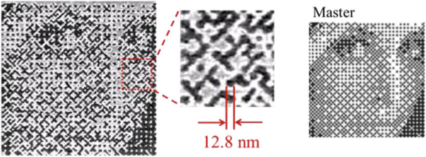
Although it was demonstrated that ferroelectric data storage at a density of approximately 10 Tbit/in2 (15.5 Pbit/m2) is possible in principle, this does not necessarily mean that actual information storage, requiring an abundance of bits to be packed together at high density, is easy to achieve. The demonstration of actual data storage with a density over 1 Tbit/in2 (1.55 Pbit/m2), which is roughly the limit of current HDD products, by using ferroelectric materials is important to show whether the technology is achievable. Figure 4 shows an SNDM image of a two-dimensional bit array written on a 40-nm-thick CLT recording medium. Actual data containing 64 × 64 bits were recorded at an areal density of 4 Tbit/ in2 (6.2 Pbit/m2). Thus, real information storage at 4 Tbit/in2 (6.2 Pbit/m2) was demonstrated with a ferroelectric medium.Reference Tanaka and Cho39
(Left) Actual data recorded at a bit spacing of 12.8 nm (areal density: 4 Tbit/in2 (6.2 Pbit/m2). (Middle) Higher resolution map. (Right) Master bit map pattern used for recording data.Reference Tanaka and Cho39

A HDD-type ferroelectric data storage test system based on SNDM has also been developed to conduct fast read/write tests.Reference Hiranaga, Uda, Kurihashi, Tochishita, Kadota and Cho40,Reference Aoki, Hiranaga and Cho41 Readout at a rate of 2 Mbps and writing at a rate of 20 Mbps were achieved using this HDD-type test system; ideal readout and writing rates for ultrahigh-density data storage are 1 Gbps. Subsequently, a higher reading speed of 10 Mbps was achieved by replacing the CLT recording medium with lead zirconium titanate, which has 70× larger nonlinear dielectric permittivity. In addition, high-density read/write demonstrations were conducted using an HDD-type test system, and writing of dot arrays with a recording density of 3.4 Tbit/in2 (5.3 Pbit/m2) was successfully demonstrated.Reference Aoki, Hiranaga and Cho41
Ferroelectric probe data storage based on field-effect transistor-type probe
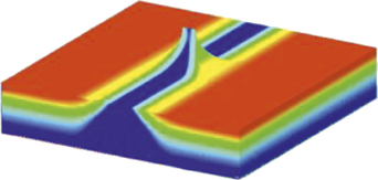
Samsung developed a ferroelectric probe data storage device based on a field-effect transistor-type probe, which they called a “resistive probe.”Reference Park, Jung and Hong42 The resistive probe has an n-type doped regions on the inclines of the tip that slightly overlap one another, whereas the body consists of p-type doped silicon (Figure 5).
(a) Schematic diagram of resistive probe in vicinity of ferroelectric thin films with up and down domains. (b) Three-dimensional dopant concentration plots for a wedge-shaped resistive probe and (c) corresponding scanning electron microscope image. Reprinted with permission from Reference Ko, Ryu, Park, Park, Kim, Jung, Min, Kim, Shin and HongReference 22. © 2011 American Chemical Society. Note: V, voltage; R, resistance; SRPM, scanning resistive probe microscope.

As one of the applications of the “resistive probe,” Samsung’s researchers reported the development of the scanning resistive probe microscope (SRPM) that has an electric field sensor aligned at the tip apex with a spatial resolution of about 200 nm and a temporal resolution of 10 ns.Reference Hong, Park, Kalinin and Gruverman1,Reference Park, Jung, Min, Kim, Hong and Shin21 However, the SRPM suffered from poor spatial resolution even though the position of the sensor was aligned with the tip apex. They found that a wedge-shaped tip has much better spatial resolution (25 nm) than a sharp tip.Reference Ko, Ryu, Park, Park, Kim, Jung, Min, Kim, Shin and Hong22,Reference Kim, Lee, Song, Lee, Park, Hong, Ko, Min, Park, Park, Jung and Shin43 The estimated upper limit of charge resolution of the SRPM was reported to be about ∼25 electrons. Checkerboard patterns of various sizes were formed by alternating up and down polarization domains, where domains of less than 25 nm in diameter could be distinguished. Therefore, the resistive probe can be used as a high-density information storage reader in ferroelectric probe storage devices with a storage density above 1 Tb/in2 (1.55 Pbit/m2).Reference Hong, Park, Kalinin and Gruverman1,Reference Park, Jung, Min, Kim, Hong and Shin21,Reference Ko, Ryu, Park, Park, Kim, Jung, Min, Kim, Shin and Hong22,Reference Tanaka, Kurihashi, Uda, Daimon, Odagawa, Hirose, Hiranaga and Cho38,Reference Ahn, Rabe and Triscone44–Reference Hong, Kim, Hong, Auciello and Wouters50
The researchers designed a ferroelectric HDD based on the resistive probe,Reference Hong, Choa, Jung, Koo and Kim51 which used an air-bearing slider to maintain an air gap of about 8 nm between the head and the medium. The front-end process of the resistive channel and conducting writer on a silicon wafer and the assembly of sliders were combined in a standard HDD head fabrication process. They also confirmed that the HDD head could be used as a writer through which voltage pulses of opposite polarities (+10 and –10 V) were applied to write alternating ferroelectric domain patterns without damage to the surface of the ferroelectric media. Kim et al. found that the writing process consists of charge injection through the air gap and polarization switching induced by the electric field exerted by the accumulated charges.Reference Kim, Bae, Ryu, Ko, Kim, Hong and Shin52 This finding can explain why the domains were written even though an air gap of 10 nm between the head and the medium existed. The air gap acts as tunneling barrier where the charges can flow, as in the case of alumina capped ferroelectric thin films.Reference Jiang, Lee, Kim and Hwang53
Summary and outlook
Today, information technology is changing rapidly and a large volume of information is produced and stored. The amount of digital information to be stored is expected to reach 40 zettabytes by 2020.Reference Gantz and Reinsel54 Electronic information and data has thus far been mainly stored in magnetic HDDs, solid-state drives, and semiconductor flash memory. In the future, it is estimated that only one-half of the total digital information produced in the world will be stored in HDD and flash memory.
Under these circumstances, new high-density storage technology beyond HDD and flash memory are needed. Some efforts have been made to develop new high-density storage technology based on scanning probe type data storage. Candidates for such scanning probe type storage include thermomechanical data storage and ferroelectric data storage.
Scanning probe type data storage still have issues to be resolved, including tip abrasion, low data reading speed per single probe tip, weakness against mechanical shock, and cost per single bit. However, these types of data storage have critical advantages in terms of higher memory density and lower cost per bit compared with competitors, such as NAND flash memory, and can overcome the challenges we described. Further efforts to resolve these disadvantages for probe data storage should be made to achieve next-generation high-density and high-capacity memories beyond HDD and flash memory to meet the continued explosion of information in 2020 and beyond.

Yasuo Cho became a full professor at the Research Institute of Electrical Communication, Tohoku University, Japan, in 2001. He received his BS degree in 1980 from Tohoku University with a degree in electrical engineering. In 1985, he became a research associate at the Research Institute of Electrical Communication. In 1990, he received an associate professorship from Yamaguchi University. He then became an associate professor in 1997 at the Research Institute of Electrical Communication. His research interests include nonlinear phenomena in ferroelectric materials and their applications, the scanning nonlinear dielectric microscope (SNDM), and using SNDM in next-generation ultrahigh-density ferroelectric data storage (SNDM ferroelectric probe memory). Cho can be reached by email at yasuocho@riec.tohoku.ac.jp.

Seungbum Hong joined the Korea Advanced Institute of Science and Technology (KAIST), South Korea, in 2017 as an associate professor in the Department of Materials Science and Engineering and created the Materials Imaging and Integration Laboratory. He received his BS degree in 1994, his MS degree in 1996, and his PhD degree in 2000 in the field of nanoscale observation of ferroelectric thin films, all from KAIST. After completing postdoctoral research at the École Polytechnique Fédérale de Lausanne, Switzerland, from 2000 to 2001, he joined the probe storage project team as a project leader at the Samsung Advanced Institute of Technology in 2002. In 2007, he moved to Argonne National Laboratory as a staff scientist, and worked as a principal investigator in local domain and transport studies of oxide heterostructures and polymer ferroelectrics using atomic force microscopy. Hong can be reached by email at seungbum@kaist.ac.kr.