I. INTRODUCTION
Neutron radiation creates two major types of radiation damage in structural materials: point defects and their clusters, Reference Was1 and transmutation induced helium (He), which can swiftly combine with vacancies to form He bubbles. Reference Reed2–Reference Lucas4 These radiation induced defects can significantly degrade the mechanical stability of irradiated metallic materials. To alleviate radiation damage in structural materials, various types of defect sinks have been investigated, including grain boundaries (GBs) Reference Han, Demkowicz, Fu, Wang and Misra5–Reference Yu, Bufford, Sun, Liu, Wang, Kirk, Li and Zhang9 and interphase boundaries. Reference Zhang, Fu, Misra and Demkowicz10–Reference Kashinath, Misra and Demkowicz14 GBs, which are unbiased sinks, Reference Misra, Demkowicz, Zhang and Hoagland12,Reference Zhernenkov, Jablin, Misra, Nastasi, Wang, Demkowicz, Baldwin and Majewski13 can mitigate radiation damage by absorbing point defects and clusters, and promoting their recombination. Reference Bai, Voter, Hoagland, Nastasi and Uberuaga15,Reference Chen, Wang, Chen and Shao16 Radiation studies on nanocrystalline (nc) metals show that defect density can be significantly reduced Reference Yu, Liu, Sun, Wang, Shao, Fu and Zhang6,Reference Song, Wu, Chen, Wang, Sun, Yu, Chen, Shao, Yang, Hartwig and Zhang17–Reference Shen, Feng, Tang, Valdez, Wang and Sickafus19 and in situ radiation provides direct evidence on defect cluster absorption by high angle GBs in nc Ni. Reference Sun, Song, Yu, Chen, Kirk, Li, Wang and Zhang20
Phase boundaries in oxide dispersion strengthened (ODS) alloys with abundant metal/oxide interfaces are critical to alleviate radiation damage and have been extensively studied. Reference Klueh, Gelles, Jitsukawa, Kimura, Odette, van der Schaaf and Victoria21–Reference Hsiung, Fluss, Tumey, Choi, Serruys, Willaime and Kimura26 Radiation responses of multilayers with well-controlled layer interfaces were increasingly investigated. Reference Zhang, Fu, Misra and Demkowicz10–Reference Misra, Demkowicz, Zhang and Hoagland12,Reference Jiao, Chen, Myers, General, Shao, Zhang and Wang27–Reference Shao, Wang, Misra and Hoagland32 In metallic multilayers, various types of interfaces have been intensively studied, including FCC/BCC interfaces (e.g., Cu/Nb, Reference Demkowicz, Misra and Caro11,Reference Misra, Demkowicz, Zhang and Hoagland12,Reference Li, Nastasi and Misra33,Reference Hattar, Demkowicz, Misra, Robertson and Hoagland34 Cu/V, Reference Fu, Carter, Swadener, Misra, Shao, Wang and Zhang35–Reference Fu, Wang, Carter, Shao, Wang and Zhang37 Cu/Mo, Reference Li, Carter, Misra, Shao, Wang and Zhang38 Cu/W, Reference Gao, Yang, Xue, Yan, Zhou, Wang, Kwok, Chu and Zhang39 Al/Nb, Reference Li, Martin, Anderoglu, Misra, Shao, Wang and Zhang40 and Ag/V Reference Wei, Li, Mara, Nastasi and Misra41,Reference Wei, Wang, Nastasi and Misra42 ), FCC/FCC interfaces (e.g., Cu/Ni, Reference Heinisch, Gao and Kurtz43 Ag/Ni, Reference Yu, Liu, Fu, Wang, Myers, Wang, Shao and Zhang44,Reference Yu, Sun, Chen, Liu, Wang, Kirk, Li and Zhang45 and Cu/FCC Co Reference Chen, Liu, Fu, Sun, Yu, Song, Li, Wang, Wang and Zhang46 ), and BCC/BCC interfaces (Fe/W Reference Li, Fu, Wang, Carter, Shao, Maloy, Misra and Zhang47 ), where FCC and BCC stand for face-centered cubic and body-centered cubic, respectively. In general, immiscible layer interfaces appear to be effective sinks to mitigate radiation induced defect clusters. Reference Zhang, Fu, Misra and Demkowicz10,Reference Zhang, Fu, Li, Misra, Wang, Shao and Wang31 In Cu/V nanolayers, the density of He bubbles and radiation hardening decline prominently with decreasing individual layer thickness h, demonstrating an appealing size effect. Reference Fu, Carter, Swadener, Misra, Shao, Wang and Zhang35–Reference Fu, Wang, Carter, Shao, Wang and Zhang37
The motivations of the current study on radiation damage in the Cu/Fe system include the followings. First, previous studies focused on radiation tolerance of incoherent immiscible metallic multilayers, and the influence of coherent immiscible interfaces on radiation tolerance remains poorly understood. It is unclear if coherent immiscible interfaces are stable during ion beam bombardment such as He ion irradiation. And if stable, can the interfaces also effectively alleviate radiation damage? Second, we reported recently that Fe in Cu/Fe multilayers undergoes a phase transformation from BCC to FCC structure when h reduces to 2.5 nm or smaller. Reference Chen, Liu, Sun, Yu, Song, Wang and Zhang48 Thus, an opportunity emerges to investigate the radiation damage in FCC/FCC multilayers with coherent immiscible interfaces. Third, Fe is the major element in ferritic/martensitic steels (FMS), primary candidates for fuel cladding materials for advanced nuclear reactors. Reference Klueh, Gelles, Jitsukawa, Kimura, Odette, van der Schaaf and Victoria21–Reference Ukai and Fujiwara25 Radiation damage in Fe-based multilayer systems may provide insights into the design of radiation tolerant FMS.
II. EXPERIMENTAL
Cu/Fe multilayers with identical h, varying from 0.75 to 100 nm, were magnetron sputtered at room temperature on HF etched Si (100) and Si (110) substrates. The chamber was evacuated to a base pressure less than 1 × 10⁻⁵ Pa, prior to deposition. Before the deposition of Cu/Fe multilayers, a 100 nm thick Cu seed layer was deposited. Detailed information was reported elsewhere. Reference Chen, Liu, Sun, Yu, Song, Wang and Zhang48 The films with various h were irradiated at room temperature using 100 keV He ions with a total fluence of 6 × 10²⁰ ions/m2. The temperature rise of the sample was ∼50 °C during implantation. The base pressure in the ion implantation system was 4 × 10⁻⁵ Pa. X-ray diffraction (XRD) experiments were performed in a Brukers D8 Discover x-ray powder diffractometer (Cu Kα radiation, Madison, WI) at room temperature. Transmission electron microscopy (TEM) experiments were carried out on a JEOL 2010 transmission electron microscope operated at 200 kV and an FEI Tecnai G2 F20 microscope operated at 200 kV with a Fischione ultra-high resolution high-angle annular dark field (HAADF) detector (FEI Company, Eindhoven, Netherlands). Cross-sectional TEM (XTEM) samples were prepared by dimpling, low energy (3.5 keV) Ar ion milling, and subsequent ion polishing. Depth-dependent damage and defect concentration profiles were calculated by the Stopping and Range of Ions in Matter (SRIM)-2008 using the Kinchin-Pease option in the SRIM software. Reference Ziegler and Biersack49
III. RESULTS
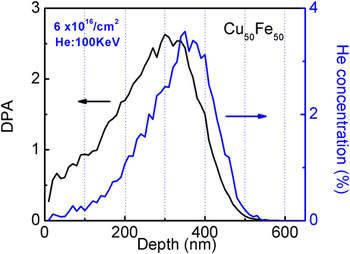
Figure 1 shows the depth profiles of radiation damage in units of displacements per atom (dpa) and helium concentration obtained from SRIM simulation of Cu50Fe50 compound subjected to He ion irradiation at 100 keV with a total fluence of 6 × 10²⁰ ions/m2. The default threshold displacement energies in the SRIM were used in the calculation. The peak damage approaches ∼2.5 dpa at a depth of ∼300 nm and the projected ion penetration depth is ∼500 nm. The peak He concentration reaches ∼3 at.% (or 30,000 appm) at a depth of ∼350 nm.
The depth profile of radiation damage in unit of dpa (left) and He concentration obtained from SRIM simulation in Cu50Fe50 subjected to He ion irradiation at 100 keV with a total dose of 6 × 10¹⁶ ions/cm2 (right). The peak damage and peak He concentration are approximately 2.5 dpa and 3 at.% (or 30,000 appm).

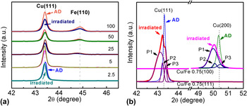
Structural evolution of multilayers before and after radiation was characterized by XRD patterns. As-deposited multilayers had incoherent interface when h ≥ 5 nm as evidenced by the co-existence of Cu (111) and Fe (110) diffraction peaks [Fig. 2(a)]. When h < 5 nm, coherency became dominant as no Fe (110) peak can be detected. When h decreased to 0.75 nm, interface was fully coherent for Cu/Fe multilayers deposited on both Si (100) and Si (110) substrates [Fig. 2(b)]. Radiation in general led to reduction of peak intensity and insignificant variation of peak positions in multilayers when h ≥ 2.5 nm as shown in Fig. 2(a). In comparison after radiation of Cu/Fe 0.75 nm multilayers, shoulder peaks appeared surrounding the original Cu (111) or Cu (200) peak for the films grown on Si (110) or Si (100) substrates. The deconvolution of each peak in irradiated Cu/Fe 0.75 nm multilayers will be discussed later.
XRD patterns of as-deposited (AD) and He ion irradiated Cu/Fe multilayers. (a) Radiation induced reduction of peak intensity and insignificant peak shift for multilayers with individual layer thicknesses varying from 2.5 to 100 nm on Si (110). Coherency between Cu and Fe became dominant when h = 2.5 nm as no BCC Fe peak can be detected. (b) When h = 0.75 nm, fully coherent (100) and (111) interfaces formed in AD Cu/Fe multilayers on Si (100) and Si (110) substrates. After radiation, shoulders appeared in prominently broadened (111) and (200) peaks, and the deconvolution of each peak displays three sub-peaks, P1, P2, and P3.

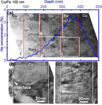
The microstructures of He ion irradiated Cu/Fe nanolayers were examined by TEM experiment. Figure 3(a) shows an XTEM micrograph of irradiated incoherent (FCC/BCC) Cu/Fe 100 nm multilayer with superimposed He concentration profile. Two boxes, b and c, were selected and magnified to examine defects in Cu and Fe layers in detail. High-density He bubbles were clearly observed in Cu [Fig. 3(b)] and Fe layers [Fig. 3(c)], which were in the peak damage area. Fe had a small columnar grain size of ∼17 nm and He bubbles appeared to distribute along the columnar GBs.
(a) A low-magnification XTEM micrograph of He ion irradiated incoherent (FCC/BCC) Cu/Fe 100 nm multilayer on Si (110) substrate, superimposed with SRIM simulated He concentration profile (blue). (b) and (c) display the microstructure of the Cu and Fe layers at higher magnification (labeled as boxes in (a)). High-density He bubbles were clearly observed. The average bubble size is ∼1.3 nm.

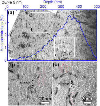
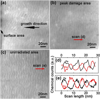
Radiation damage in Cu/Fe 5 nm multilayers was examined in parallel. A panoramic view of the irradiated film is shown in Fig. 4(a). The depth dependent He concentration profile is embedded in the same figure. He bubbles appeared to distribute along the wavy layer interfaces. The magnified images at the two locations, close to surface and peak damage, are shown in Figs. 4(b) and 4(c). It is evident that a large number of He bubbles were aligned along Cu/Fe interfaces. Scanning transmission electron microscopy (STEM) experiments were performed to examine irradiated multilayers at various locations, close to surface [Fig. 5(a)], peak damage [Fig. 5(b)], and unirradiated region beyond the projected ion range [Fig. 5(c)]. Layer interfaces were clearly discernable throughout the entire irradiated multilayer. Comparisons of compositional line profiles between the peak damage [Fig. 5(d)] and unirradiated area [Fig. 5(e)] show modulated variation of Cu and Fe compositions across layer interfaces, implying insignificant intermixing after He ion irradiation.
(a) A panoramic XTEM micrograph of He ion irradiated Cu/Fe 5 nm multilayer on Si (110) substrate with embedded He concentration profile. (b) and (c) display magnified images of the box b and c labeled in (a). (b) Most He bubbles were aligned along interfaces. (c) Bubble density increased and Cu/Fe interfaces became preferred locations for He bubbles. The average bubble size is ∼1.8 nm.

Cross-sectional scanning TEM (STEM) micrographs of irradiated Cu/Fe 5 nm multilayer film on Si (110) substrate showing microstructures at three locations: (a) close to surface, (b) peak damage area, and (c) unirradiated area. Layer interface retained in irradiated multilayers. (d) Comparisons of compositional line profiles obtained from the peak damage area in (b) and unirradiated area in (c) show modulated variation of Cu and Fe compositions across layer interface, implying insignificant intermixing after He ion radiation.

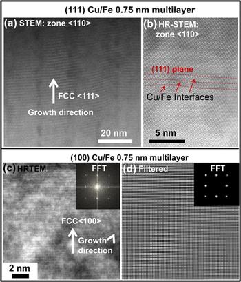
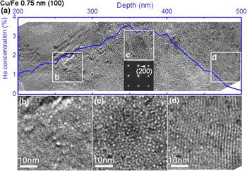
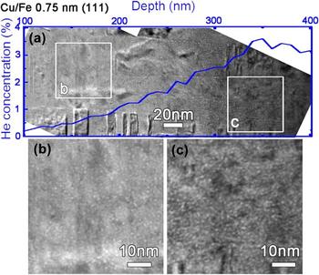
TEM examinations of irradiated fully coherent Cu/Fe 0.75 nm multilayers on Si (110) [Fig. 6(a)-6(b)] and Si (100) [Fig. 6(c)-6(d)] substrates were also conducted to investigate the radiation response of coherent immiscible interfaces. Before radiation, STEM and HRSTEM micrographs in Fig. 6(a)-6(b) confirm that as-deposited (111) textured Cu/Fe 0.75 nm multilayers are fully coherent with chemically abrupt layer interfaces. Similarly the HRTEM micrograph and filtered image with fast Fourier transform in Fig. 6c-d revealed the formation of coherent interface, indicating that Fe has undergone phase transformation from BCC to FCC Fe. Figure 7(a) displays an XTEM micrograph that overviews the microstructure of He ion irradiated fully coherent (100) Cu/Fe 0.75 nm multilayer accompanied by the SRIM simulated He concentration profile. Three boxes, b–d, were magnified to examine radiation damage in detail at higher magnification. Close to surface [Fig. 7(b)], low-density He bubbles were randomly distributed. High-density He bubbles appeared in the peak damage area [Fig. 7(c)]. Although no clear layer interfaces were discernible in the surface and peak damage areas, the irradiated multilayer retained fully coherent and single-crystal-like microstructure as indicated by the embedded selected area diffraction (SAD) pattern in Fig. 7(a). In the region close to the end of He concentration profile [Fig. 7(d)], the layer interface in irradiated Cu/Fe 0.75 nm multilayers retained, and arrays of low-density He bubbles (with a diameter of ∼1 nm or less) with an average separation distance of 1.5 nm were observed. The smaller size of He bubbles (compared to those in thicker multilayers) appears to be curtailed by the individual layer thickness. Furthermore, if bubbles reside at layer interfaces, the average spacing of arrays of He bubbles should be 0.75 nm. Thus, we speculate that He bubbles may nucleate primarily within the layers. In irradiated coherent (111) Cu/Fe 0.75 nm multilayer, high-density growth twins were visible [Fig. 8(a)], whereas layer interface cannot be easily distinguished along this zone axis. Radiation damage close to the surface [Fig. 8(b)] and in peak damage zone [Fig. 8(c)] also revealed abundant He bubbles, similar to those observed in irradiated (100) Cu/Fe 0.75 nm multilayer. The irradiated (111) Cu/Fe 0.75 nm multilayers remained highly coherent and epitaxial.
(a) A STEM image of as-deposited (111) Cu/Fe 0.75 nm multilayer showing chemically abrupt layer interfaces. (b) A high-resolution STEM image revealing coherent interfaces between Cu and Fe. (c) A high-resolution TEM image and (d) FFT-filtered image displaying coherent interfaces between Cu and Fe in as-deposited (100) Cu/Fe 0.75 nm multilayer. Fe in both systems has undergone phase transformation from BCC to FCC Fe.

(a) A panoramic XTEM micrograph that overviews the microstructure of He ion irradiated fully coherent Cu/Fe 0.75 nm multilayer on Si (100). The evolution of bubble density is consistent with the superimposed He concentration profile (blue curve). (b), (c), and (d) display the respective magnified images of the irradiated films at locations b–d shown as boxes in (a). (b) Close to surface, low-density bubbles were randomly distributed. (c) High-density He bubbles appeared in the peak damage area. No clear layer interfaces were observed in both (b) and (c). However, the structure remained fully coherent and single-crystal-like, as shown in the embedded SAD pattern in (a). (d) In the region close to the end of He concentration profile, layer interface retained, and arrays of low-density He bubbles (with a diameter of ∼1 nm or less) with an average separation distance of 1.5 nm were observed. The smaller size of He bubbles (comparing to those in thicker multilayers) appears to be curtailed by the individual layer thickness. Furthermore, if bubbles reside at layer interfaces, the average spacing of aligned arrays of He bubbles should be 0.75 nm. Thus, we speculate that He bubbles may nucleate primarily within the layers.

(a) An XTEM micrograph that overviews the microstructure of He ion irradiated fully coherent Cu/Fe 0.75 nm multilayer on Si (110). The evolution of bubble density is consistent with the superimposed He concentration profile (blue curve). (b) and (c) display the respective magnified images of the irradiated films at locations b and c shown as boxes in (a). (b) Close to surface, bubbles were randomly distributed. (c) High-density He bubbles formed in the peak damage area. No clear layer interfaces were detected in both (b) and (c).

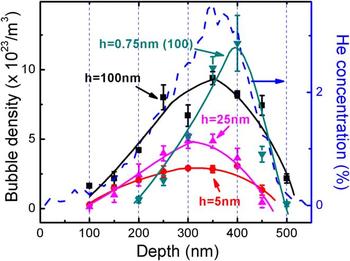
Statistical distributions of He bubble density versus penetration depth in several irradiated Cu/Fe multilayers are compared in Fig. 9. Overall, the evolution of He bubble density followed that of He concentration profile (the dashed line), that is, the He bubble density increased with radiation depth and approached maxima where the He concentration also achieved a maximum value and decreased rapidly thereafter. The He bubble concentration profiles of Cu/Fe 0.75 nm on two types of Si substrates were similar, and hence only one of them is shown for clarity.
A statistical study of He bubble density distribution versus penetration depth in irradiated Cu/Fe 100, 25, and 5 nm multilayers on Si (110) substrates and Cu/Fe 0.75 nm multilayer on Si (100) substrate. The evolution of He bubble density matched closely to that of He concentration profile.

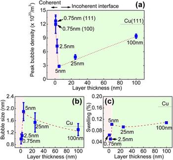
The peak bubble density in multilayers [as shown in Fig. 10(a)] decreased continuously with decreasing h, reached a minimum value when h = 5 nm, and bounced back up rapidly when h < 5 nm. Meanwhile, the average bubble size [Fig. 10(b)] and swelling [Fig. 10(c)] in multilayers were also compared to obtain a comprehensive knowledge of size dependent radiation damage. Careful examination of Fig. 10(b) shows that with decreasing h, the average bubble size increased from 1.2 to a maximum of 1.8 nm when h = 5 nm and decreased rapidly thereafter to a minimum of ∼1 nm when h = 0.75 nm. From the measured average bubble density and size, we estimated swelling (due to He bubbles) in Fig. 10(c). When h is in the range of 5–100 nm, swelling did not vary significantly, but remained lower than that of monolith Cu (shown by the horizontal dashed line). Swelling decreased when h = 2.5 nm and increased slightly with further decrease of h to 0.75 nm.
(a) The variation of peak He bubble density with layer thickness h shows that with the decrease in h, the peak bubble density firstly decreases continuously and reaches a minimum value when h = 5 nm, and bounces back rapidly when h < 5 nm. The peak bubble densities of Cu/Fe 0.75 multilayers are comparable to those of pure Cu films. (b) The evolution of bubble size has an opposite trend to that of peak bubble density. (c) Swelling is estimated based on the bubble densities and sizes. When h = 5–100 nm, swelling does not change significantly. The optimized swelling reaches at h = 2.5 nm and the magnitude of swelling bounces back slightly with further decrease of h to 0.75 nm.

IV. DISCUSSION
A. Radiation response of incoherent Cu/Fe interfaces at large layer thickness (h ≥ 5 nm)
Immiscible multilayer systems with FCC/BCC incoherent interfaces have been widely investigated,
Reference Zhang, Fu, Misra and Demkowicz10–Reference Misra, Demkowicz, Zhang and Hoagland12,Reference Zhang, Fu, Li, Misra, Wang, Shao and Wang31
as abundant layer interfaces serve as effective defect sinks
Reference Misra, Demkowicz, Zhang and Hoagland12
without significant radiation induced intermixing.
Reference Zhang, Fu, Misra and Demkowicz10,Reference Zhang, Fu, Li, Misra, Wang, Shao and Wang31,Reference Fu, Misra, Wang, Shao and Zhang36,Reference Li, Martin, Anderoglu, Misra, Shao, Wang and Zhang40,Reference Li, Fu, Wang, Carter, Shao, Maloy, Misra and Zhang47
Examination of microstructures of He ion irradiated Cu/Fe multilayers with h in the range of 5–100 nm reveals a size dependent reduction of average and peak He bubble density. The average bubble spacing L (estimated by
 $L = 1/{N^{1/3}}$
, where N is bubble density) escalates from ∼10 nm in the Cu/Fe 100 nm multilayer to 16 nm in the irradiated Cu/Fe 5 nm multilayer. Incoherent Cu/Fe interfaces act as defect sinks and provide the recombination/annihilation sites for radiation induced point defects/defect clusters. Similar phenomena have been reported in He ion irradiated FCC/BCC systems, such as Cu/V,
Reference Fu, Carter, Swadener, Misra, Shao, Wang and Zhang35,Reference Fu, Misra, Wang, Shao and Zhang36
Cu/Nb,
Reference Misra, Demkowicz, Zhang and Hoagland12,Reference Li, Nastasi and Misra33
and Cu/Mo,
Reference Li, Carter, Misra, Shao, Wang and Zhang38
and FCC/FCC multilayers, such as Ag/Ni.
Reference Yu, Liu, Fu, Wang, Myers, Wang, Shao and Zhang44,Reference Yu, Sun, Chen, Liu, Wang, Kirk, Li and Zhang45
As the bubble density significantly deceases with decreasing layer thickness, a natural question arises: where are He atoms distributed in multilayers? As the solid solubility of He in crystal lattice is exceptionally low, Reference Reed2–Reference Lucas4 a majority of He atoms could be located either at layer interfaces or within He bubbles. Atomistic explanation of He storage at multilayer interfaces has been provided in Cu/V and Cu/Nb multilayers by molecular dynamics. Reference Kashinath, Misra and Demkowicz14 Our previous studies Reference Chen, Liu, Sun, Yu, Song, Wang and Zhang48 identified two types of interfaces in FCC/BCC Cu/Fe multilayers, a primary Kurdjumov–Sachs (K–S) and secondary Nishiyama–Wasserman (N–W) orientation relationship. He atoms should be stored at these interfaces in the form of either nanoscale platelets Reference Kashinath, Misra and Demkowicz14 or stable He-vacancy clusters. Reference McPhie, Capolungo, Dunn and Cherkaoui50 It is worth mentioning that the combination of vacancies with trapped He atoms at layer interfaces leads to the nucleation of He bubbles along interfaces.
Another interesting phenomenon is that, in the Cu/Fe 5 nm multilayer, the average bubble size [Fig. 10(b)] (∼1.8 nm) is slightly larger than that in Cu/Fe 100 nm (∼1.3 nm), which implies that fast diffusion of He atoms and point defects to layer interfaces when h is small promotes the preferred bubble nucleation and growth at interfaces. Since bubbles mostly stay at Cu/Fe 5 nm multilayer interfaces, we will use a simple thermodynamic model to estimate the bubble pressure at interface. Note that bubbles in irradiated Cu/Fe at room temperature have spherical shape [Fig. 4], which is different from the lenticular shape of bubbles at GBs or at layer interfaces during high temperature radiation. Reference Trinkaus and Singh51 For a gas-filled bubble with radius R, embedded in a matrix, the change of free energy of the matrix due to the bubble is given by, Reference Was1
 $${\mathop{\rm d}\nolimits} G = V{\mathop{\rm d}\nolimits} p + \gamma {\mathop{\rm d}\nolimits} A\quad {\rm{,}}$$
where V is the volume of bubble, p is the outward pressure of gas, γ is the surface tension of bubble, and A is the area of bubble surface. If a spherical bubble resides at interface, the growth of the bubble is accompanied by reducing the interface area and as a result, Eq. (1) can be modified as
 $${\mathop{\rm d}\nolimits} G = V{\mathop{\rm d}\nolimits} p + \gamma {\mathop{\rm d}\nolimits} A - {\gamma _{{\rm{Int}}}}{\mathop{\rm d}\nolimits} A\prime \quad {\rm{,}}$$
where γInt is the interface energy, A′ is the interface area consumed by the bubble, and it follows that
 $$V{\mathop{\rm d}\nolimits} p = {\mathop{\rm d}\nolimits} \left( {pV} \right) - p{\mathop{\rm d}\nolimits} V\quad {\rm{.}}$$
For an ideal gas, pV = constant and
 $V = 4/3\pi {R^3}$
, A = 4πR
2, A′ = πR
2. Then,
 $${{{\mathop{\rm d}\nolimits} G} \over {{\mathop{\rm d}\nolimits} R}} = - 4\pi R\left( {p - {{2\gamma } \over R} + {{{\gamma _{{\rm{Int}}}}} \over {2R}}} \right)\quad {\rm{.}}$$
At equilibrium state (dG/dR = 0),
 $$p = {{2\gamma } \over R} - {{{\gamma _{{\rm{Int}}}}} \over {2R}}\quad {\rm{.}}$$
Second term on the right indicates that at equilibrium state, bubble pressure at interfaces is lower than that in matrix. Knowing the surface energy of the bubble in Cu [∼1.77 J/m2 (Ref. Reference Tyson and Miller52)] and Cu/Fe interface energy [∼0.44 J/m2 (Ref. Reference Hough and Rolls53)], we can estimate the bubble pressures in the Cu/Fe 100 nm multilayer (matrix) and Cu/Fe 5 nm multilayer (most bubbles located at interface) as ∼5.3 and 3.7 GPa. Thus, we conclude that bubble pressure at interface in multilayers with smaller h (h = 5 nm) is lower than that inside multilayers with larger h (h = 100 nm).
B. Radiation response of incoherent Cu/Fe interfaces at small layer thickness (h < 5 nm)
Radiation tolerance of immiscible FCC/FCC metallic multilayer systems was barely studied as few such systems have immiscibility. Prior studies on He ion, proton, and Kr ion irradiated Ag/Ni multilayers with large lattice mismatch (∼14%) show multilayers with smaller h having lower defect density after radiation. Reference Yu, Liu, Fu, Wang, Myers, Wang, Shao and Zhang44,Reference Yu, Sun, Chen, Liu, Wang, Kirk, Li and Zhang45 Foregoing study indicates that immiscibility and incoherency are two important factors to design an interface with superior radiation tolerance. To date, however, little is known on the radiation response of coherent immiscible interfaces as it is a challenge to design coherent immiscible interfaces in metallic materials. Significant solid solubility typically prevails in metallic systems with the same crystal structure and nearly identical lattice parameters, such as Cu/Ni, Reference Liu, Bufford, Wang, Sun and Zhang54 Ag/Au, Reference Wonnell, Delaye, Bibolé and Limoge55 Ag/Al, Reference Bufford, Bi, Jia, Wang and Zhang56,Reference Bufford, Liu, Zhu, Bi, Jia, Wang and Zhang57 or Fe/Cr Reference Baibich, Broto, Fert, Van Dau, Petroff, Eitenne, Creuzet, Friederich and Chazelas58 multilayer, which are vulnerable to prominent intermixing during radiation. Due to epitaxial growth of FCC Fe on Cu in Cu/Fe multilayers, the immiscibility and coherency criteria can both be satisfied, providing a rare opportunity to study the radiation response of coherent immiscible interfaces.
The critical layer thickness for the formation of misfit dislocations in FCC Cu/Fe multilayer is estimated to be ∼3 nm, Reference Chen, Liu, Sun, Yu, Song, Wang and Zhang48 considering the magnitude of the Burgers vector b as 0.25 nm and the mismatch strain εm as 0.83%. Coherent Cu/Fe interfaces start to dominate when h = 2.5 nm and complete coherency is achieved when h = 0.75 nm.
The He bubble density escalates with decreasing h or increasing coherency when h < 5 nm [Fig. 10(a)]. The bubble density in fully coherent Cu/Fe 0.75 nm multilayer is comparable to that in monolithic Cu. However, the average bubble size in fully coherent Cu/Fe 0.75 nm multilayer is smaller than multilayers with larger h and monolithic Cu [Fig. 10(b)], indicating that fully coherent interface can still mitigate radiation damage by effectively curtailing the bubble size. It is worth mentioning that the increase of bubble density with decreasing h could not be attributed solely to the coherency at layer interfaces. At smaller h, the bubble size is also curtailed by the layer thickness. Hence, a higher bubble density will be necessary to accommodate the same concentration of implanted helium. Furthermore, the magnitude of bubble induced swelling is lower in Cu/Fe 2.5 nm multilayer than the multilayers with larger h.
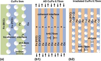
An intriguing phenomenon observed in irradiated Cu/Fe 0.75 nm multilayer is that bubbles reside frequently in Cu layers as shown in Fig. 7(d). Such peculiar radiation response may be ascribed to relaxation of coherency strain and modulus difference between Cu and FCC Fe. First, in as-deposited coherent FCC Cu/Fe 0.75 nm multilayer, Cu is under compression and Fe is under tension with a coherency strain of ∼0.83% [Fig. 11(b)]. As the formation of bubbles introduces tensile strain, Reference Fu, Misra, Wang, Shao and Zhang36 the bubbles may prefer to accumulate in Cu layers that are under compression to release strain energy. XRD results in Fig. 2(b) reflect the structural evolution of (100) and (111) Cu/Fe 0.75 nm multilayers before and after radiation. After radiation, the fully coherent diffraction peak in Cu/Fe 0.75 nm multilayers can be deconvoluted into three peaks, with the respective strain of ∼0.5% (P1), 0.2% (P2), and −0.1% (P3) near the (111) peak in (111) Cu/Fe 0.75 nm multilayer. Similarly, the strain in three deconvoluted peaks is ∼0.7% (P1), 0.5% (P2), and −0.2% (P3) in the (100) Cu/Fe 0.75 nm multilayer. We suspect that P1, P2, and P3 are associated with irradiated Cu layers with confined bubbles, coherency peak between irradiated Cu and Fe, and irradiated FCC Fe layers, respectively. After radiation, the relaxation of coherency strain results in the separation of Cu and Fe peaks. Second, the shear modulus of Cu (μCu = 48 GPa) is lower than that in Fe (µFe = 77.5 GPa). Thus, it may be easier to nucleate bubbles in Cu than in Fe. As the average layer thickness of Cu is 0.75 nm, the average bubble diameter is in the same range, ∼1 nm, much smaller than those observed in other Cu/Fe multilayers with greater h.
(a) Schematics illustrate that in incoherent Cu/Fe 5 nm multilayer, He bubbles align predominantly along layer interfaces. (b1) Prior to radiation of fully coherent immiscible Cu/Fe 0.75 nm multilayer, Cu is under compression and Fe is under tension. (b2) After radiation, He bubbles prefer to nucleate in Cu layers and are constricted to reside inside Cu layers.

Foregoing discussions suggest that bubble size is effectively curtailed by layer thickness in coherent immiscible multilayers, resulting in a substantial decrease of swelling. Coherent immiscible layer interfaces also play an essential role in mitigating radiation damage.
V. CONCLUSION
A systematic study on radiation response of immiscible Cu/Fe multilayers with incoherent and coherent layer interfaces was performed. At large layer thickness (h ≥ 5 nm), incoherent Cu/Fe interface is stable and enables significant reduction of He bubble density. At smaller layer thickness (h ≤ 2.5 nm) when coherency prevails, the bubble density increases. However, the average bubble size is substantially curtailed by fully coherent immiscible interfaces, leading to reduced swelling. Therefore, this study suggests that coherent immiscible interfaces can also prominently alleviate radiation damage.
ACKNOWLEDGMENTS
We acknowledge financial support by NSF DMR-1304101. This work was performed, in part, at the Center for Integrated Nanotechnologies (CINT), a U.S. Department of Energy Nanoscience user facility, jointly operated by Los Alamos and Sandia National Laboratories. Los Alamos National Laboratory, an affirmative action equal opportunity employer, is operated by Los Alamos National Security, LLC, for the National Nuclear Security Administration of the U.S. Department of Energy under contract DE-AC52-06NA25396. HAADF-STEM was performed by Dr. Yuanyuan Zhu at the National Center for Electron Microscopy at Lawrence Berkeley National Laboratory, which is supported by the Office of Science, Office of Basic Energy Sciences of the US Department of Energy (Contract DE-AC02-05CH11231). Access to microscopy and imaging center (MIC) at Texas A&M University is also acknowledged.