I. INTRODUCTION
Modern communications, wireless and broadcast standards like long term evolution (LTE) [1], 802.11ac WiFi [2] and digital video broadcasting (DVB) [3] require radio frequency (RF) power amplifiers (PAs) to achieve a high degree of signal fidelity at high efficiency. High efficiency results in low power consumption, which for mobile phone users means longer battery life and for network operators and broadcasters lower electricity bills.
A number of architectures exist for increasing RF PA efficiency including Doherty [Reference Hone4], Outphasing/linear amplification using non-linear components (LINC) [Reference Hone, Aref, Guan and Negra5], Dynamic Load Modulation [Reference Mimis and Watkins6] and envelope tracking (ET) [Reference Kim7]. Doherty is particularly popular for narrowband applications. It can be used over large frequency ranges, but generally requires two RF input signals or significant digital pre-distortion (DPD). ET on the other hand has proven itself to be frequency agile and has recently been incorporated into a number of commercially available mobile phone handsets [8], validating its commercial acceptance.
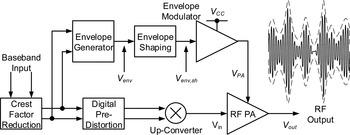
ET achieves high system efficiency by dynamically controlling the supply voltage to an RF amplifier in sync with the transmitted signal as shown in Fig. 1. The peak-to-average power ratio (PAPR) of the incoming baseband quadrature modulation (IQ) data is first reduced with crest factor reduction (CFR). The CFR can consist or simply clipping the signal peaks – as done in this work – which has little effect on the average envelope power. From here a normalized envelope signal (V env ) is generated by calculating its magnitude. This is then processed with envelope shaping (ES) to produce V env,sh which is amplified by the envelope modulator to drive the RF PA with (V PA ). The envelope modulator must be: high-speed, linear, and power efficient if good system performance is to be achieved. DPD is also often applied to the baseband data before up-conversion to correct for any non-linearities in the RF PA.
General layout of envelope tracking RF PA. Modulator transfer response.

This paper is an extended version of [Reference Watkins and Mimis9]. It is organized as follows: First the charge pump ET system is described and its efficiency improvement is analyzed. Next its practical implementation is described and finally practical results are presented.
II. SUPPLY SWITCHING/TRACKING
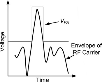
Although split frequency envelope modulators [Reference Kim7] are capable of producing over 60% total system efficiency from power supply to RF output (DC-to-RF) when combined with the right RF PA, they are complex and cannot be easily integrated because they contain inductors, and sometimes transformers. The inductors tend to be large in value, resulting in large physical size and high cost. Linearity can also suffer due to distortion introduced around the cross-over frequency between the high and low frequency paths. To combat this, a number of more simple architectures have emerged based on simply switching the supply voltage between multiple levels [Reference Augeau10], or linearly tracking between two [Reference Walling, Taylor and Allstot11] or more [Reference Kim, Son, Kim and Park12]. Linear tracking tends to perform better, since switching introduces noise, which degrades the adjacent power ratio (ACPR). Most published designs require additional power supplies, which are undesirable in mobile devices, multiple-input-multiple-output (MIMO) systems or future 5 G systems based on Massive MIMO arrays [13]. This work linearly tracks between two voltages for the sake of simplicity, although a greater number of voltages would improve efficiency [Reference Kim, Son, Kim and Park12], but at the cost of complexity. The basic operation of a supply switching modulator is shown in Fig. 2, where V PA switches in sync with the envelope of the RF carrier voltage.
Operation of an envelope modulator with multiple supply voltages.

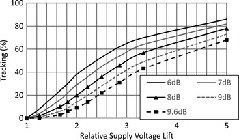
It is assumed that the lower value of V PA is equal to the supply voltage (V CC ), so increasing V PA around the peaks is defined as the supply voltage lift. In Fig. 2 V PA increases with a ratio of 1:2, therefore the supply voltage lift is two times relative to V CC . The possible efficiency for a given relative supply voltage lift was simulated with a 5 MHz LTE signal and quadrature phase shift keying (QPSK) modulation. The original 9.6 dB PAPR was reduced with clipped CFR. CFR increases efficiency, but also degrades signal fidelity. The RF PA is assumed to be a class AB with a peak efficiency of 70%. The results are shown in Fig. 3.
Efficiency of supply switching/tracking ET RF PA and modulator for a given PAPR.

The modulator in Fig. 3 is assumed to be ideal. For a given relative supply voltage lift there is an optimum PAPR for maximum efficiency. If V PA is doubled, the optimum PAPR is 6 dB, leading to a DC-to-RF efficiency improvement of 13% points from 31 to 44%. PAPR is generally higher than 6 dB, and for the original 9.6 dB PAPR signal, 2.5 times is optimum.
So far a supply voltage switching envelope modulator has been considered. Whether supply switching or linear tracking is used, it makes little difference to the simulated efficiency as presented in Fig. 3. It is assumed in the linear tracking mode that the RF PA operates in or close to its saturated region during the tracking phase. Therefore, two distinct modes of operation exist: linear with a fixed supply voltage, and saturation with supply voltage tracking. In Fig. 2 V PA switches infrequently to the higher value, as would linear supply tracking. When not tracking, and in the linear mode with fixed supply voltage region, any distortion generated is equal to that of a class AB PA, which is generally less than an ET PA. This is analyzed in Fig. 4, where the percentage of tracking operation is shown for a given signal PAPR and relative supply voltage lift.
Percentage of ET operation for a given PAPR.

As the relative supply voltage lift increases, the ratio of the upper to lower supply voltage also increases, leading to a larger degree of tracking, since the envelope signal spends more time above the lower supply voltage. There also exists an inverse relationship with signal PAPR, since a high PAPR signal will have less frequent peaks than a low PAPR signal. Therefore an ET PA, which tracks the least, will on an average produce less distortion. It is another parameter, which should be considered when designing ET PAs and transmitters [Reference Mimis and Watkins6].
III. CHARGE PUMP MODULATOR
An alternative approach to tracking between multiple power supplies is a linear capacitive charge pump [Reference Marston14] that doubles the V PA around the peaks [Reference Watkins and Mimis9, Reference Watkins15]. In [Reference Watkins15] the whole envelope signal range is tracked, requiring two analog inputs, hence two digital-to-analog converters and associated baseband. The solution shown in Fig. 5 [Reference Watkins and Mimis9] only requires one analog input.
Charge pump modulator.

A push-pull class-B PA drives a capacitor C 1 with voltage V PPA in a charge pump configuration as described in [Reference Watkins and Mimis9]. The use of a linear class-B amplifier instead of a switch, allows V PA to track the peaks of the envelope instead of just switching between two discrete levels [Reference Augeau10]. If the charge pump is ideal with zero voltage drop across the components, then V CC is doubled during the peaks. V PA therefore swings between V CC and twice V CC . Figure 3 suggests that 40% DC-to-RF efficiency is possible for this configuration with an 8 dB PAPR signal.
A) ES
The charge pump architecture lends itself to ES since only the signal peaks are tracked. Assuming a perfect charge pump modulator capable of doubling V CC then only the upper 50% of V env is tracked. A conditional branch is used to only pass V env to the push-pull class B PA when it exceeds a threshold. Below this, V PA is fixed at V CC minus the voltage drop of D 1, therefore not tracking the nulls:
 $${V_{env,sh}}{\rm =} \left\{ {\matrix{ {{V_{env}}} & {{V_{env}}{\rm \gt 0}{\rm. 5}} \cr {{\rm 0}{\rm. 5}} & {{V_{env}} \le {\rm 0}{\rm. 5}} \cr}} \right\}.$$
This results in a harsh transition – referred to as a “clipped” function – which can degrade the ACPR [Reference Watkins15]. Watkins [Reference Watkins15] also shows that ACPR can be improved with a “curved” function to smooth the transition between linear and tracking regions. Equation (1) has been normalized to a peak value of 1 as shown in Fig. 6 for both functions, alongside an unshaped one.
Envelope shaping functions.

The curved function shown in Fig. 6 “kicks in” at 0.3 leading to a low “fit” between V PA and the RF output [Reference McCune16] and therefore degrading efficiency. In this work the normalized curved function kicks in at 0.4 V, which is chosen to be close to the clipped to maximize efficiency. Here it is calculated digitally and uploaded to a signal generator, but could also be generated in the analog domain with a diode-resistor piecewise non-linear function [Reference Sedra and Smith17]. It is given by:
 $${V_{env,sh}} = \left\{ {\matrix{ {{\rm 0}{\rm. 97} \cdot {{\left( {{V_{env}} - {\rm 0}{\rm. 4}} \right)}^{1.3}} + {\rm 0}{\rm. 5}} & {{V_{env}} \gt 0.4} \cr {{\rm 0}{\rm. 5}} & {{V_{env}} \le 0.4} \cr}} \right\}$$
The shaping function is arbitrarily chosen here. Often, more sophisticated algorithms are used based on the different operating regions of the RF PA [Reference McCune16].
ES has a secondary function in linearizing the PA. Because it ensures that the transistor always operates above its “knee” voltage, transconductance collapse and large variations in the transistor's drain-source capacitance [Reference Kim, Moon and Kim18] are avoided. The latter has two effects: first the matching to the transistor will not be optimum over the whole V PA range, and secondly phase distortion (AM–PM) is generated. Limiting the minimum value of V PA with ES reduces these effects.
IV. PRACTICAL IMPLEMENTATION
The charge pump ET RF PA was built on a single FR4 printed circuit board as shown in Fig. 7. The RF PA is at the bottom with input on the left, output on the right, and the modulator above it. CFR was applied off-line and from this V env is generated. ES was also applied off-line. V env,sh and the IQ data were loaded into a LeCroy Arbstudio arbitrary signal generator. The IQ was then up-converted with a HP8780 vector signal generator. The board was designed with jumpers so that the modulator and RF amplifier could be independently tested.
Charge pump ET; inputs on left, output with attenuator on right, RF amplifier along bottom of board and modulator above it.

An Analog Devices AD8013 dual op-amp IC was used for the push-pull amplifier in Fig. 5. The AD8013 is an asymmetric digital subscriber line (ADSL) driver with a high output current capability. Its two halves are connected in parallel to double the output current. Even so, under high output currents, significant voltage drop appear across the output stage. Based on its datasheet, 1 V voltage drop is estimated and 0.5 V was assumed for the Schottky diode D 1 in Fig. 5.
With 12 V V CC the nominal value of V env when not tracking a peak was 11.5 V. During this phase the output of the push-pull amplifier (V PPA ) was 1 V above ground. This is the charging phase for C 1. A total of 1.5 V was dropped, charging it to 10.5 V. When tracking the peaks, the maximum V PPA will be 11 V (accounting for voltage drops). This would theoretically result in a peak V env of 21.5 V, equivalent to an absolute supply voltage lift of 1.87 times or only tracking the top 5.5 dB of the peaks. This architecture favors a low PAPR, however to maintain signal fidelity the PAPR was clipped at 8 dB. With regard to Fig. 3, 41% DC-to-RF efficiency is estimated and the peaks were only tracked 16% of the time. Timing misalignment between the two paths in an ET PA can be a major source of ACPR degradation. Watkins and Mimis [Reference Watkins and Mimis19] show that tolerance to timing misalignment is increased when ES prevents tracking into the nulls. Therefore, only tracking the envelope 16% of the time should result in good average linearity, even if the two paths are slightly misaligned.
A) Charge pump capacitor
During the peaks C 1 must hold sufficient charge to prevent its voltage (V C1) “drooping”, resulting in clipped peaks and distortion being introduced. By analyzing the 5 MHz LTE signal, the largest duration of a peak was 5 µs. It is assumed that the peak has a semi-sinusoidal shape above the nominal V PA as shown in Fig. 8(a).
Peak tracking (a) V PA and (b) V C1.

The simplest approximation for C 1's voltage droop is a constant current draw by the RF PA. This results in a linear droop as shown in Fig. 8(b). However, as V PA decreases over the duration of the peak, its current consumption will fall, suggesting that a constant resistive load impedance (R L ) is a better approximation. This is more complex since the droop is non-linear with more current drawn at the maximum excursion of the peak. This was analyzed with:
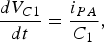 $$\displaystyle{{d{V_{C1}}} \over {dt}} = \displaystyle{{{i_{PA}}} \over {{C_1}}},$$
where i PA is the current flowing into the RF PA. Combining (3) with Ohms law where R L is the drain impedance of the RF PA:
 $$\displaystyle{{d{V_{C1}}} \over {dt}} = \displaystyle{{{V_{PA}}} \over {{R_L} \cdot {C_1}}}.$$
V PA is the sum of V C1 and V PPA . The latter is assumed to be a semi-sinusoid:
 $$\displaystyle{{d{V_{C1}}} \over {dt}} = \displaystyle{1 \over {{R_L} \cdot {C_1}}}({V_{C1}} + A \cdot Sin(\omega t + \theta )).$$
A is the peak amplitude of V PPA – 11 V in the example above. Equation (5) can be solved numerically by breaking the peak up into equally spaced samples of duration τ. dV C1 on the left side of the equation is the difference between the current V C1 and the previous value (separated by τ), i.e. V C1,n and V C1,n−1 and V C1 on the right is the average value of V C1,n and V C1,n−1:
 $$\displaystyle{{{V_{C1,n - 1}} - {V_{C1,n}}} \over \tau} = \displaystyle{1 \over {{R_L} \cdot {C_1}}}\left( {\displaystyle{{{V_{C1,n - 1}} + {V_{C1,n}}} \over 2} + A \cdot Sin\left( {\displaystyle{{\pi \cdot {\tau _n}} \over t}} \right)} \right),$$
t is the period of the peak (5 µs in this example). τ n is the relative time between 0 and t. Equation (6) was simulated to analyze how the value of C 1 impacts the peaks with the assumptions given above, and that R L is 50 Ω [Reference Watkins15]. The voltage drop of V C1 over 5 µs is shown in Fig. 9(a), where the greatest gradient is at 2.5 µs, as suggested by Fig. 8. The impact on V PA is shown in Fig. 9(b), where distortion to the envelope signal increases over time, introducing memory effects. To maintain signal fidelity, two 4.7 µF ceramic capacitors in parallel were used for C1 resulting in 9.4 µF and minimum distortion. A larger value would have less droop, but take up more board space.
(a) Voltage droop across C1, and (b) its impact on V PA during the peaks.

B) RF PA
The RF PA was designed to operate at 710 MHz with a class AB bias and exhibit a drain impedance of 50 Ω. A PD85004 laterally diffused metal oxide semiconductor (LDMOS) transistor was chosen, the schematic of which is shown in Fig. 10. Design of RF amplifiers for ET applications is not trivial as V env tracks the envelope, the gate-source capacitance (C gs ) of the transistor changes. This is similar to C ds mentioned above, introducing a mismatch and further AM–PM distortion [Reference Rahkonen, Hietakangas and Aikio20]. This can be compensated for, by tuning the input matching network of the PA. Normally, at a fixed bias condition the RF PA is tuned for maximum gain. C gs will have one value under these conditions. At a different series of bias conditions, C gs will be a different value, leading to a mismatch and reduced gain. This gain variation is termed the AM–AM distortion. In this work the RF PA is intentionally mismatched to flatten the gain response over whole dynamic range of V PA , therefore minimizing the ACPR.
Schematic of the RF PA.

V. RESULTS
The charge pump modulator was initially evaluated with a fixed 50 Ω load for R L to emulate the RF PA drain impedance, and the 8 dB 5 MHz LTE shaped envelope signal applied to its input. The transfer response of this is shown in Fig. 8. The voltage drop of D 1 and the push-pull amplifier was greater than the estimated 1.5 V, resulting in a V PA swing between 11.3 and 20.2 V. This is equivalent to tracking the top 5.1 dB of the signal peaks. Even so, the response shown in Fig. 11 is fairly linear with only a small degree of clipping at the ends of the signal excursions. The normalized root mean square error (NRMSE) between V PA and V env,sh was −37.5 dB.
Modulator transfer response.

With a fixed supply voltage of 11.5 V, the RF amplifier achieved a peak efficiency of 71.7% at its 3 dB compression point and 34.2 dBm P OUT under continuous wave excitation. The equivalent drain impedance was 36 Ω. Backing-off the PA, it still operates in the linear region with 49 Ω drain impedance resulting in an efficiency of 53.7% at 31.6 dBm P OUT .
Applying the 5 MHz LTE signal and the clipped ES function, the input match to the ET PA was retuned for the optimum gain/ACPR trade-off. By sacrificing 3 dB gain, a 6 dB improvement in ACPR was possible. The first channel ACPR under these conditions was −30.4 dBc. This meets the evolved UMTS terrestrial radio access (E-UTRA) emission mask for LTE handsets of −30 dBc [Reference Kim7] without the need for any DPD, making this a “DPD Lite” PA. The second channel ACPR was −38.9 dBc. P OUT was 31.3 dBm (1.36 W) and the DC-to-RF efficiency 42.9%. The curved ES function improved the ACPR to −32.5 dBc, but at a reduced efficiency of 38.9%. The input power (P IN ) with the 5 MHz LTE signal was swept and the results presented in Fig. 12 against P OUT for both the clipped (1) and curved (2) ES functions.
Charge pump ET power sweep with 5 MHz LTE signal.

The curved function has better ACPR, as suggested by [Reference Watkins15], although the clipped function was more efficient due to the improved “fit” between V PA and the output signal. There exists a trade-off in the ES function between efficiency and linearity.
Both handset and basestation PAs exhibit power control to reduce power consumption and limit interference to other users [Reference Yan, Draxler, Presti, Kimball and Asbeck21]. At low P OUT , performance of the ET PA was better with the modulator disabled. It then operates permanently in linear fixed supply mode with zero modulator power consumption and smaller maximum P OUT . Therefore an extended mode is proposed whereby under low transmit powers, ET operation is disabled to reduce power consumption [Reference Kang22].
The two ES function were evaluated under different operating modes: First, with the clipped ES focusing on efficiency and an ACPR threshold of −30 dBc. Secondly, the curved function focusing on ACPR with efficiency a secondary parameter. The first operating mode is shown in Fig. 13 over a 15 dB power control range, where ET is only used over the top 3.7 dB of its operating range. When ET is enabled the ACPR drops immediately, as does the efficiency due to the tracking of the peaks.
Dual mode charge pump ET power sweep with 5 MHz LTE signal and clipped ES function.

In the tracking region a supply lift of 1.87 times is always applied to V PA even when not operating at maximum P OUT . Efficiency could be improved further if the magnitude of the supply lift was tracked in harmony with P OUT . The AM–AM and AM–PM at maximum P OUT are shown for clipped ES function in [Reference Watkins and Mimis9], where a kink is visible as the PA passes from the linear to tracking region.
The second operating mode with the curved function achieved better linearity than the clipped function shown in Fig. 13, although under large backed-off there was little difference between them. Under these conditions shown in Fig. 14 the ACPR is below −36 dBc except at very high P OUT , where it climbs to −32.5 dBc. The point at which ET is enabled and disabled in Fig. 14 is at a lower threshold than that of Fig. 13, to meet the enhanced linearity requirement.
Dual mode charge pump ET power sweep with curved ES function and 5 MHz LTE signal.

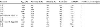
ET operation now occurs over the top 8 dB operating range when the curved ES function aims to maximize linearity. A comparison with other supply switching/tracking architectures is given in Table 1, where this work can be seen to achieve the highest efficiency for an ET PA using either one or two power supplies.
Comparable architectures.

It should be noted that [Reference Walling, Taylor and Allstot11] is a pure complementary metal oxide semiconductor (CMOS) design, which would be expected to have a lower efficiency due to stray parasitics. It also used DPD to improve linearity. Similarly, [Reference Kim23] has a CMOS modulator, but a GaAs RF PA. Watkins [Reference Watkins15] is also based on a charge pump structure, but is more complex, since it tracks the whole dynamic range of the envelope with two analog inputs. In [Reference Kim, Son, Kim and Park12] a number of different configurations are presented based on two, three, and four supply voltages. It is more linear and efficient, but at the cost of greater complexity with additional power supplies, which take up significant circuit board area.
VI. CONCLUSION
A simple ET architecture is described here, intended to increase the efficiency and linearity of an RF PA by only tracking the peaks of the transmitted signal. The theory shows that by simply doubling the supply voltage to the RF PA around the peaks, efficiency can be increased by 10–15% points for high PAPR signals.
To minimize complexity a modulator based around a capacitive charge pump is proposed, which can accomplish this voltage doubling with only a single power supply voltage making it a compact design suitable for miniaturization and integration.
When used with a clipped ES function and no DPD the complete ET amplifier achieved 42.9% efficiency at 1.36 W output power with an 8 dB PAPR 5 MHz bandwidth LTE signal. The ACPR was −30.4 dBc meeting the LTE emission mask for handsets. ACPR can be improved with a curved ES function, but at the expense of reduced efficiency. Efficiency under back-off power control could be increased by disabling the modulator and just operating from a fixed supply voltage. Compared with similar work published elsewhere, this amplifier achieves the highest performance in its class.
ACKNOWLEDGEMENTS
The authors would like to thank all at Toshiba Research Europe Limited for their support of this work.
 Gavin Tomas Watkins is a member of both the Institute of Engineering Technology and the European Microwave Association. He received the MEng degree in Electrical and Electronic Engineering in 2000 from the University of Bristol and a Ph.D. from the same institution in 2003 on the topic of Wideband Feedforward Amplifiers for Software defined Radios. From 2003 to 2004, he was a technical consultant for Detica Information Intelligence before joining the University of Bristol as a research associate. Since 2008 he has been with Toshiba Research Europe Limited where he is currently a Research Fellow and responsible for defining and overseeing a number of RF related projects. His research interests include linear power amplifiers, high efficiency system architectures, analogue circuitry, high speed power switching architectures and wideband RF structures.
 Konstantinos Mimis received M.Sc. and Ph.D. degrees from the University of Bristol, Bristol, UK, in 2008 and 2013, respectively. Since 2012 he has been with Toshiba Research Europe Limited, Bristol, UK. His research interests include high efficiency, broadband power amplifier design, amplifier linearization and efficiency enhancement techniques.