Introduction
The gain of a transmitting antenna in a wireless communication system can be increased to expand wireless coverage range, lower error rates, achieve higher bit rates, and require less battery life from wireless communication devices. Aligning the polarization of the transmitting and receiving antennas is a critical component that enhances this gain. To guarantee this kind of polarization alignment, the transmitter and the receiver must have the same axial ratios, spatial orientations, and polarization sensors. However, maintaining constant spatial orientation alignment becomes almost impossible in mobile and portable wireless applications, as devices regularly change positions and orientations. Because the radiated waves oscillate in a circular pattern perpendicular to the propagation direction, circularly polarized (CP) antennas provide an alignment option for a broad range of orientations.
CP microstrip antenna development involves a number of design stages and obstacles. The antenna must first be built to operate at a particular frequency. It then achieves CP by either adding a perturbation segment to a basic single-fed microstrip antenna or using two feeds of the same magnitude but physically 90∘ phase offset. To ensure that the antenna attains an axial ratio of less than 3 dB at the intended design frequency, the shape and dimensions of perturbation must be optimized.
It has been observed that three different approaches have been used to increase the 3 dB axial ratio bandwidth of patch antennas that are CP. The antenna aperture area is used in the first method [Reference Zhang, Zhu and Liu1, Reference Liu, Zhu and Choi2]. A suspended structure that has a lower effective permittivity to define the radiating area is proposed in [Reference Liu, Zhu and Choi2]. But this architecture is extremely susceptible to mistakes in the installation height of the suspension. Furthermore, this method uses a dual-fed methodology to accomplish CP, requiring a sophisticated supplementary feed network. In order to offset radiation gain at low elevations, the next technique adds more radiation components, such as surface waves [Reference Bao and Ammann3] and vertical currents [Reference Son, Park, Lee, Jin and Oh4]. Regrettably, unregulated surface waves have a detrimental effect on the wireless communication system as a whole, and the radiators vertical components result in a design that is high profile. The third is the application of enhanced ground structures, like cavity-backed [Reference Zuo, Yang and Zhang5] and three-dimensional (3D) ground configurations [Reference Tang, Chiou and Wong6]. Nonetheless, the high-profile design is the outcome of these nonplanar grounds.
In recent years, the most popular techniques used for 3D printing are – (a) stereolithography apparatus (SLA) [Reference Li, Wu, Li, Chen, Yan and Zhang7, Reference Palomares-Caballero, Alex-Amor, Valenzuela-Valdés and Padilla8] which is an effective method for the improvement of antenna technology [Reference Wu, Abdelrahman, Liang, Yu and Xin9–Reference Huang, Zhou, Sim, Chio and Yuan13]; (b) fused deposition modeling (FDM) technology or fused filament fabrication (FFF) technology is preferred to reduce cost and time in fabrication of the antenna [Reference Liang, Shemelya, MacDonald, Wicker and Xin20–Reference Aksimsek, Ozek and Ozpinar23]; (c) digital light processing [Reference Colella, Chietera and Catarinucci21] technology is faster than SLA.
This letter presents a new design for a microstrip patch antenna that uses 3D printed substrate technology to achieve CP and a wide 3 dB axial ratio beamwidth (ARBW). In particular, because of its strength, longevity, and user-friendliness, FDM technology or FFF technology is utilized for 3D printing with acrylonitrile butadiene styrene (ABS) for antenna manufacturing [Reference Muntoni17–Reference Liang, Shemelya, MacDonald, Wicker and Xin20]. The permittivity of the ABS is 2.7, and its loss tangent is 0.005. A dual-purpose hexagonal mesh-grid structure composed of thermoplastic material and air is used to form the substrate. First, the insertion of two thermoplastic chunks into the substrate creates an imbalance that makes it easier to generate CP waves. Second, by varying the volume proportion of air, the effective permittivity of substrate can be modified, which in turn affects the 3 dB ARBW. The effectiveness of the suggested strategy is validated by testing and manufacturing a prototype, the results of which demonstrate a high degree of agreement between simulated and measured outcomes.
Geometry of the proposed antenna
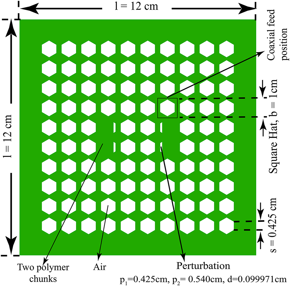
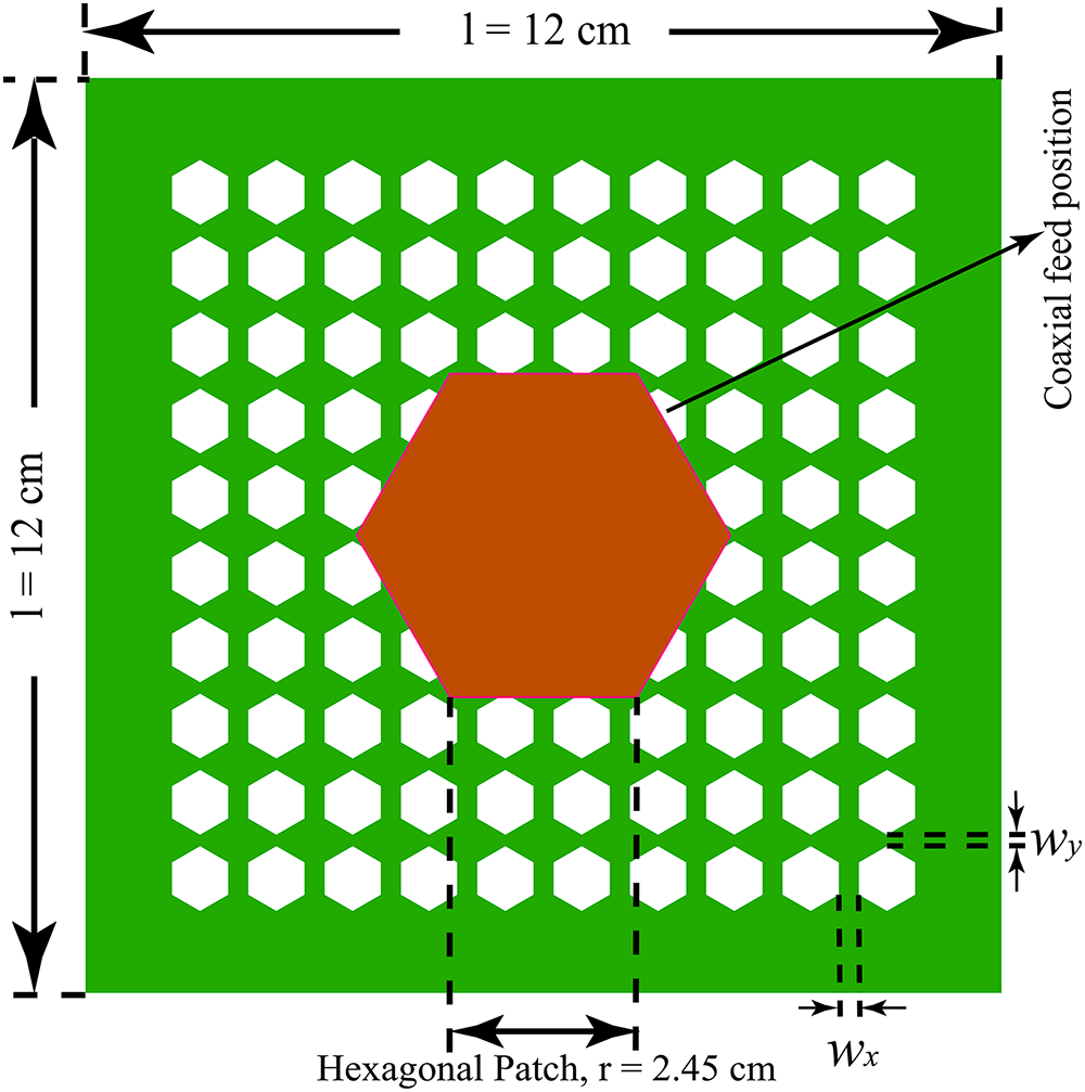
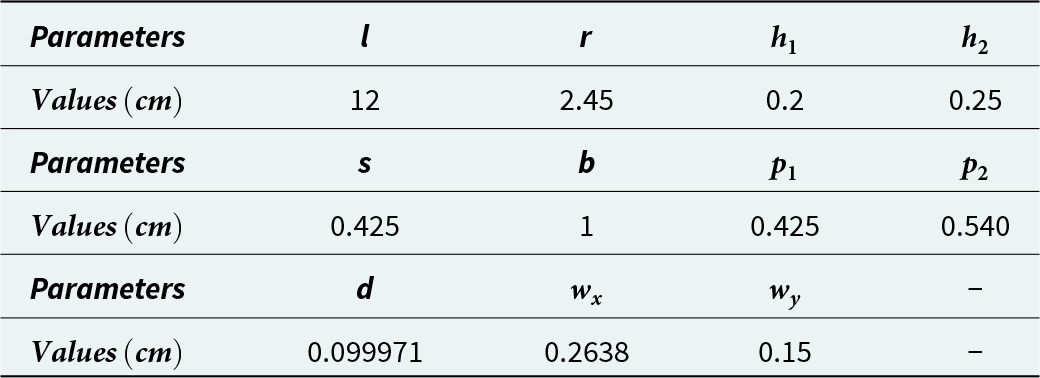
The suggested single-fed CP patch antenna’s layer-by-layer layout is shown in Fig. 1. While the substrates and ground have square geometries with side length denoted as l, the patch has a hexagonal structure with radius r. To increase impedance matching to the coaxial feed at 50 Ω, a square top-hat is placed beneath the patch along its diagonal, occupying two layers of the substrate. The top hat square has side dimension b. The symbols h 1 and h 2, respectively, represent the thicknesses of the upper and lower layers. The perturbation in the lower layer has the shape of a trapezium with dimensions p 1, p 2, and d, where p 1 and p 2 are the parallel sides and d represents the distance between the two parallel lines. The top view of the lower layer and the upper layer of 3D printed substrate is shown in Figs. 2 and 3. To make installation easier, the two layers are joined with an industrial adhesive. Table 1 represents a list of the specific measurements for the suggested antenna.
The exploded view of the proposed single-fed CP antenna with 3D printed substrates.

Top view of the lower layer of air-filled 3D printed ABS substrate.

Top view of the upper layer of 3D printed ABS substrate with hexagonal patch.

Dimensions of the proposed antenna

A hexagonal mesh-grid structure with a side length of s, for each cell, makes up the inner portion. All cells contain air, with the exception of two pairs that are symmetrically positioned along the median line in the x-direction. Two rectangular thermoplastic polymer solids are partially filled in these particular cells and are positioned in the xy plane at a distance d from the nearby polymer wall. Furthermore, the thicknesses wx and wy denote the space between two neighboring air-filled cells, in x and y directions, respectively.
Operating principle
Generation of CP
In contrast to linear polarization, which involves rigorous oscillation in a single plane, CP involves the electric field vector of the electromagnetic wave rotating in a circular pattern as it propagates. In order to transform linearly polarized waves into CP waves, the CP antennas do not require an additional external component. An external polarizer could be required in linearly polarized antennas in order to change the broadcast or polarization of received signal from linear to circular. But without the requirement for such an external component, single-fed CP antennas are made in a way that allows them to emit CP waves naturally
 \begin{equation}
f_{x}=2W_{x}\sqrt{\epsilon_{rx}}
\end{equation}
 \begin{equation}
f_{y}=2W_{y}\sqrt{\epsilon_{ry}}.
\end{equation}
In light of this characteristic, single-fed CP antennas are more straightforward and efficient because they do not require extra parts, which could lower system costs, complexity, and possible points of failure. They can also provide easier integration and installation into systems when CP is required. Numerous single-fed CP patch antenna structures, including almost square patches, truncated corner patches, and patches loaded with slots or stubs, have been proposed over the last 30 years. These documented CP patch antennas work on the fundamental idea of shaping a square patch in order to produce uneven effective lengths in two orthogonal directions.
In this paper, an alternative method is used to stimulate CP radiation as seen in Fig. 2, the substrate under the patch is printed with varying effective permittivity in different directions. The two ABS solids were introduced, having longer side lengths in the y-direction than the x-direction. This results in a slightly lower relative permittivity, denoted as ϵrx and ϵry.
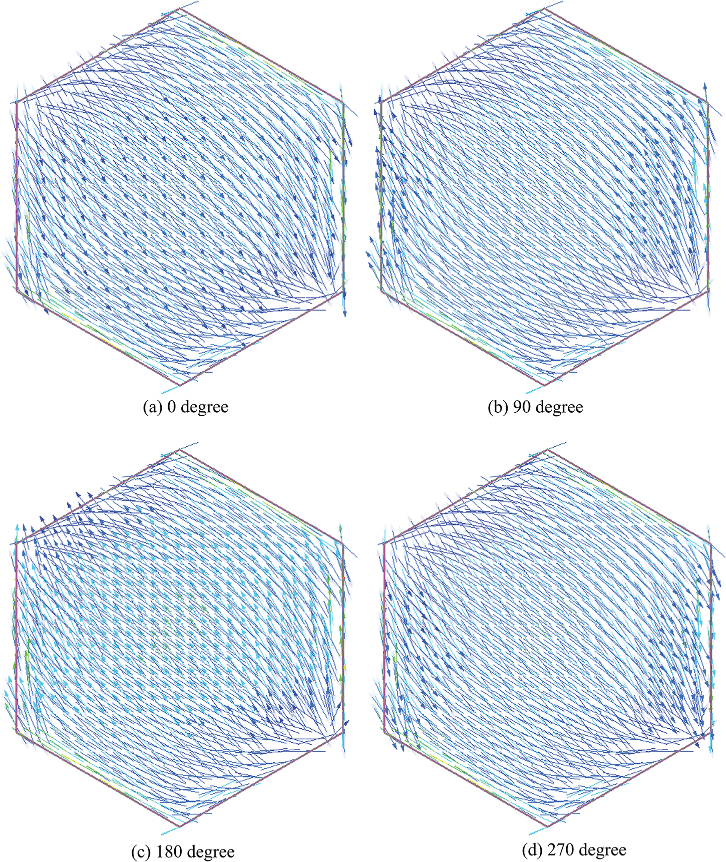
As a result, as (1) and (2) predicts, the two degenerate modes can be somewhat separated, demonstrating that the effect of the perturbation on shape is identical to that of the difference in effective permittivities [Reference Jackson14]. Alternatively, the substrate produces the appropriate perturbation for CP rather than the patch. Figure 4 illustrates the distribution of surface current on the patch during a time interval T, with the same interval t = T/4 at 2.4 GHz. This shows that the left-hand circular polarization (LHCP) of CP patch antenna is realized as anticipated.
Surface current distribution on the patch at 2.4 GHz at (a) 0 degree, (b) 90 degree, (c) 180 degree and (d) 270 degree.

Generation of wide beamwidth
In this article, an electromagnetically coupled feeding technique is used to generate CP in order to counteract the influence of probe feed on radiation properties. To produce LHCP, the feed phases progressively rise in clockwise direction at intervals of 90∘. This CP patch antenna can be conceptualized as an array of two pairs of parallel magnetic currents in a square shape, in accordance with the traditional patch antenna theory [Reference Balanis15]. Therefore, the normalized far-field components of two orthogonal electric fields, Ex and Ey, can be written as follows in the xz and yz planes:
 \begin{equation}
E_{x}=\cos(\pi\sin{\theta}W_{e}/{\lambda})
\end{equation}
 \begin{equation}
E_{y}=(\sin(\pi \sin(\theta)W_{e}/{\lambda}))/(\pi \sin(\theta)W_{e}/{\lambda})\cos(\theta).
\end{equation}
Here, We is the effective patch width and λ is the free-space wavelength. Assuming that the quadrature phase is precisely stimulated in Ex and Ey, AR can be obtained as
 \begin{equation}
AR = |{20\log_{10} (E_{x}/E_{y} )}|.
\end{equation}
It is evident from (3), (4), and (5) that AR depends on  $W_{e}/{\lambda}$. Furthermore, the electrical width of a patch antenna operating in the dominant TM 01 mode can be expressed as
 \begin{equation}
W_{e} = {\lambda}/2 \sqrt{(\epsilon_{reff})}
\end{equation}
and
 \begin{equation}
\epsilon_{reff} = [\epsilon_{r} + 1]/2 + [\epsilon_{r} - 1] * [1 + 12h/W_{p} ]^{-1/2}/2.
\end{equation}
Here, ϵr denotes the relative permittivity of the substrate and ϵreff denotes the effective relative permittivity of the resulting patch antenna. As a result,  $W_{e}/{\lambda}$ depends on ϵr, h, and Wp in accordance with equations (6) and (7). The relative permittivity of the substrate is the only factor that may define the 3 dB ARBW of the resulting antenna, which has a constant side length.
In order to meet the practical design requirement for a freely achievable value of relative permittivity of the substrate, a hexagonal mesh-grid substrate is manufactured using 3D printing technology, as illustrated in Fig. 2. With a relative permittivity of 2.7, ABS makes up the walls of the air-filled cells in the substrate. Therefore, the volume fractions of the two different types of materials can be used to regulate the effective permittivity of this mesh-grid substrate. The effective relative permittivity of the whole substrate can be computed using the Landau and Lifshitz–Looyenga equation (8) [Reference Nelson16]
 \begin{equation}
(\epsilon_{r})^{1/3} = v_{1} (\epsilon_{r1})^{1/3} + v_{2} (\epsilon_{r2})^{1/3}
\end{equation}
where v 1 and v 2 are the volume fractions of the corresponding components, indicated by  $z/(z + z_{s})$ and
 $z_{s}/(z + z_{s})$, and
 $\epsilon_{r1}$ and
 $\epsilon_{r2}$ are the relative permittivities of the thermoplastic material and air, respectively. Additionally, the effective permittivity is computed and derived with the assistance of ANSYS HFSS
 $^{TM}$.
Parametric study
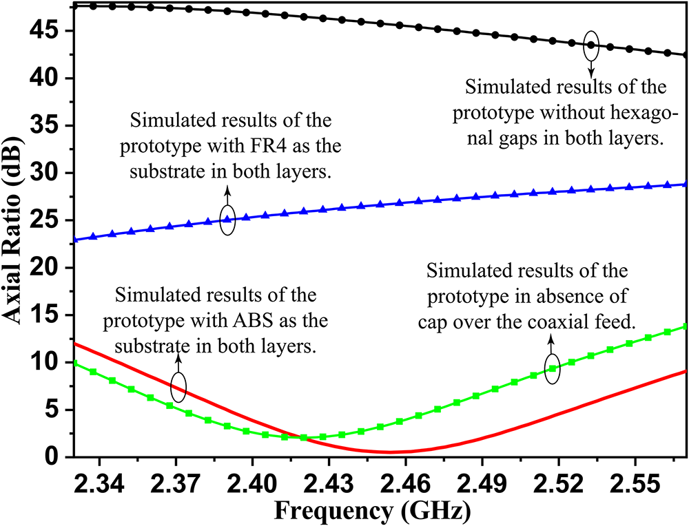
It was observed that using FR4 as the substrate material decreases the antenna gain from 7.01 dB to 4.81 dB. Figure 5 compares simulated results of the axial ratios of fabricated CP antenna prototype for the following cases, when: (i) ABS material is used as a substrate in both layers; (ii) FR4 material is used as a substrate in both layers; (iii) in absence of cap over the coaxial feed; (iv) without hexagonal gaps in both layers.
Comparison of simulated results of the axial ratios of fabricated CP antenna prototype, when: (i) ABS material is used as a substrate in both layers; (ii) FR4 material is used as a substrate in both layers; (iii) in absence of cap over the coaxial feed; (iv) without hexagonal gaps in both layers.

Figure 6 illustrates the comparison of simulated results of the reflection coefficients of fabricated CP antenna prototype for the following cases, when: (i) ABS material is used as a substrate in both layers; (ii) FR4 material is used as a substrate in both layers; (iii) in absence of cap over the coaxial feed; (iv) without hexagonal gaps in both layers.
Comparison of simulated results of the reflection coefficients of fabricated CP antenna prototype, when: (i) ABS material is used as a substrate in both layers; (ii) FR4 material is used as a substrate in both layers; (iii) in absence of cap over the coaxial feed; (iv) without hexagonal gaps in both layers.

Introducing a hexagonal mesh structure in the substrates achieved the desired results for both axial ratio and reflection coefficient, compared to substrates without the hexagonal mesh.
Additionally, the antenna gain and reflection coefficients, for simulated and measured values, were compared for antenna designs with and without the hat on the coaxial feed. It was found that the antenna design without the hat on the coaxial feed resulted in lower antenna gain.
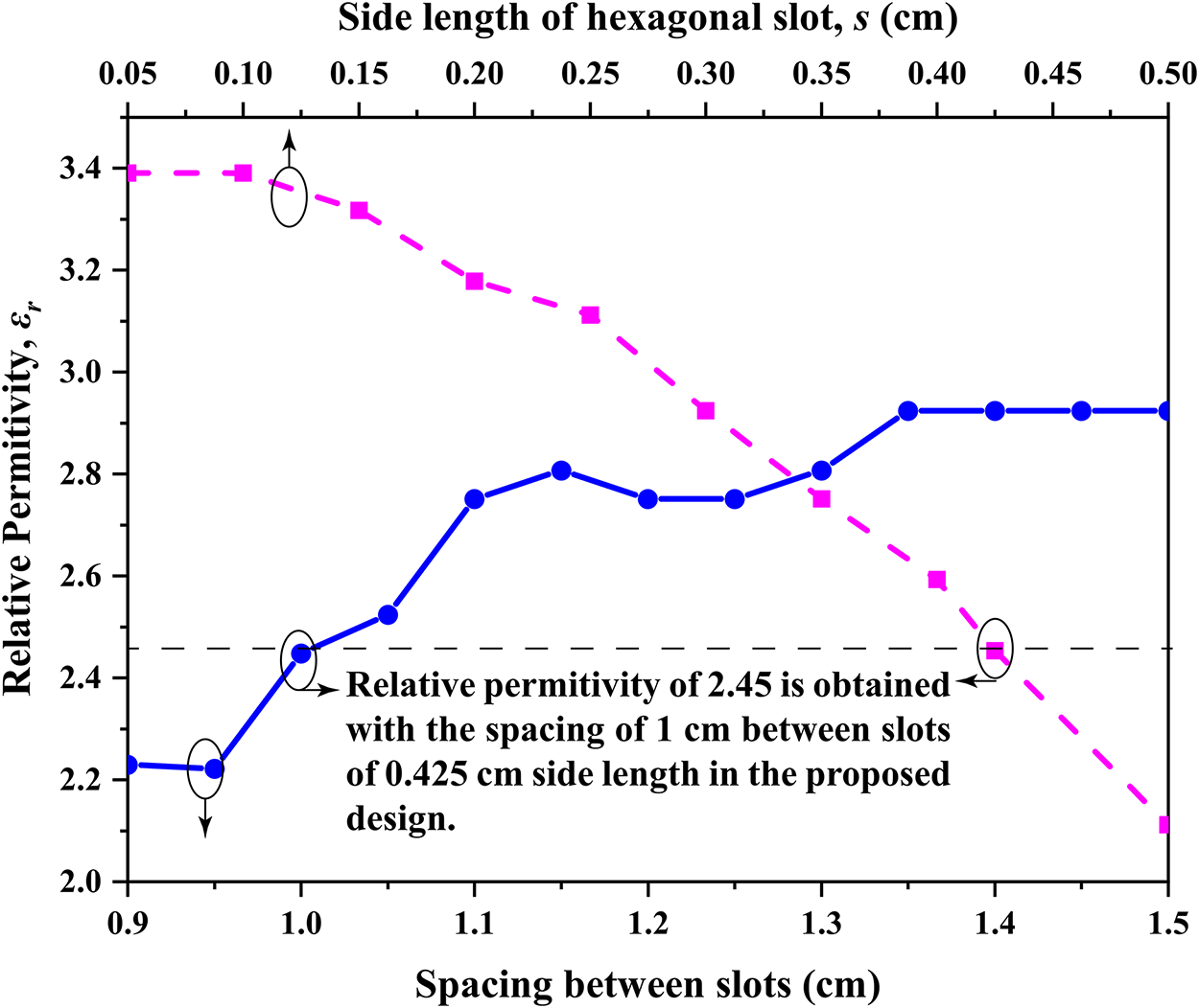
Further the parametric study of the variation of relative permittivity ϵr by varying spacing between hexagonal slots of the substrate for the suggested patch antenna was studied and secondly the variation of the relative permittivity ϵr of the substrate while varying the side length or the size of the hexagonal slots in the substrate was studied as shown in Fig. 7. Relative permittivity of 2.45 was obtained with the spacing of 1 cm between the hexagonal slots of 0.425 cm side length in the proposed design.
Parametric study of variation of relative permittivity, ϵr with spacing between slots (cm) and variation of relative permittivity and side length of hexagonal slot,  $s\,(cm)$.

Fabrication and experimental results
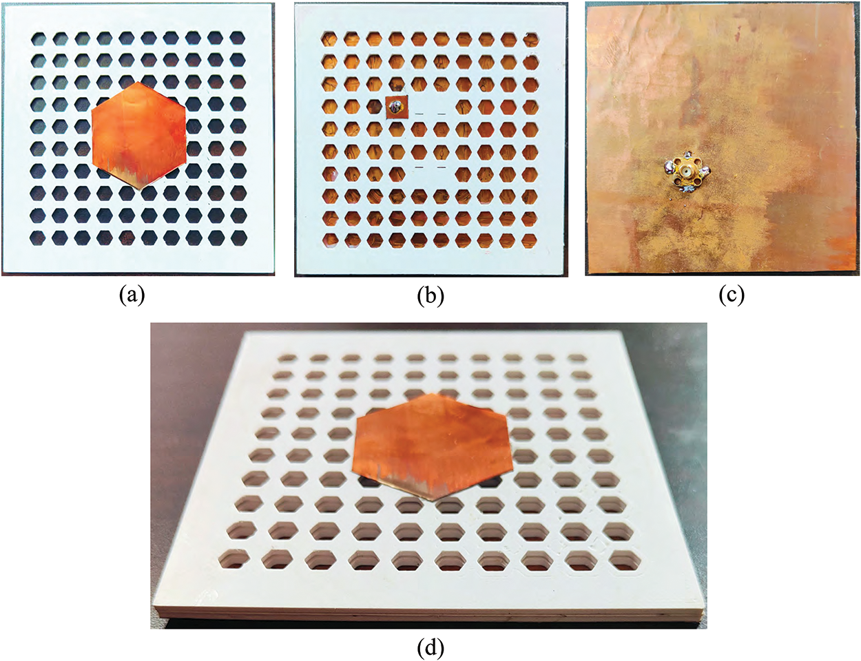
The photos of 3D printer setup for the fabrication of the double layer substrate is shown in Fig. 8, the antenna prototype in Fig. 9 displays the hexagonal mesh-grid structure of the 3D printed substrate. Experimental setup for the 3D printed antenna is displayed in Fig. 10. The ground plane, 3D printed substrate, and patch are all parts of the structure, which is put together by attaching them with industrial glue and secured. The top hat is precisely inserted into the substrate, indicating that the suggested structure of patch antenna is sufficiently stable.
3D printer setup for the double layer substrate.

(a) 3D printed upper layer, (b) 3D printed lower layer, (c) ground with coaxial feed, (d) 3D printed prototype of CP patch antenna.

Experimental setup for the 3D printed antenna.

The measured and simulated axial ratio advances of the manufactured prototype are shown in Fig. 11. The lowest measured and simulated ARs at broadside are discovered to be 0.64 dB and 0.54 dB at 2.43 GHz and 2.45 GHz, respectively. Their respective AR bandwidths are  $3.46\%$ and
 $3.6\%$.
Simulated and measured axial ratios of the fabricated CP antenna prototype.

The measured and simulated values of reflection coefficients of the constructed CP antenna prototype are displayed in Fig. 12 and there is a good agreement between the two. Additionally, there is a good match between the measured and simulated 10 dB impedance bandwidths, which span from 2.362 GHz to 2.503 GHz and 2.357 GHz to 2.467 GHz, respectively.
Simulated and measured reflection coefficients of the fabricated CP antenna prototype.

Simulated and measured normalized radiation patterns of the fabricated CP antenna prototype at  $\phi=0^\circ$ and
 $\phi=90^\circ$ are shown in Figs. 13 and 14 shows the simulated LHCP and right-hand circular polarization (RHCP) plots of the fabricated CP antenna prototype. The LHCP radiation gain is more than the RHCP gain and its value is 4.99 dB. The antenna has a 3 dB ARBW of 176∘, which is evidently broad enough to satisfy the wide beamwidth requirements for a range of practical applications.
Simulated and measured normalized radiation patterns of the fabricated CP antenna prototype at  $\phi=0^\circ$ and
 $\phi=90^\circ$.

Simulated LHCP and RHCP plots of the fabricated CP antenna prototype.

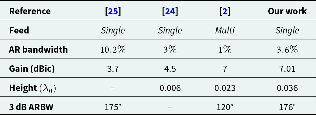
The comparative study between previous works and our work has been provided in Table 2. From the comparison, it is evident that the proposed antenna has a simple structure with low profile, moderately high antenna gain, wide AR bandwidth and 3 dB ARBW.
Comparison between previous works and our work

Conclusion
Using an innately asymmetric mesh realization grid substrate, a novel single-fed CP patch antenna operating on 2.4 GHz with high gain of 7.01 dBic is proposed in this letter. Four unique cells arranged along one median line of the substrate allow for the realization of the intended asymmetry for CP radiation with LHCP of 94 MHz axial ratio bandwidth (2.409–2.503 GHz). FDM technology is used as a typical approach for 3D printing to fabricate the substrate of the low profile proposed antenna having 10 dB impedance bandwidth of 110 MHz (2.357–2.467 GHz) which helps to incorporate this proposed antenna in various applications such as IoT and smart devices, intelligent transport systems, and GPS tracking.
Acknowledgements
The fabrication of the proposed antenna was facilitated by the AICTE-IDEA Laboratory (developed under the Grant-in-Aid under the scheme All India Council of Technical Education-IDEA Lab, India; grant no. AICTE/IDEA202000139/2021), Dr. B. C. Roy Engineering College, Durgapur, West Bengal, India and Intelligent System Engineering Laboratory, CSIR-Central Mechanical Engineering Research Institute, Durgapur – 713209, India.
Competing interests
The authors report no conflict of interest.

Monalisa Pal received her B.E. degree in Electronics and Telecommunication Engineering from Vinayaka Missions University, AVIT, Chennai, Tamil Nadu in the year 2009. Master of Technology degree in Modern Communication Engineering from Dr. B.C. Roy Engineering College, Durgapur, West Bengal in the year 2012. She is currently pursuing Ph.D. in Engineering from AcSIR at CSIR – Central Mechanical Engineering Research Institute, Durgapur, West Bengal, India, since 2023. She has 8 years teaching experience as an Assistant Professor in Electronics and Communication Engineering Department at Bengal College of Engineering, Durgapur. Her research interests include planar antenna, microwave filters, wireless communication, and intelligent transport systems applications.

Umesh Shrikrishna Patkar completed his doctoral research at the National Institute of Technology, Durgapur, India. He is currently serving as a Senior Principal Scientist at the Central Mechanical Engineering Research Institute (CMERI) in Durgapur, a national laboratory under the Council of Scientific and Industrial Research (CSIR), Ministry of Science and Technology, Government of India and Assistant Professor of Academy of Scientific and Innovative Research (AcSIR), Ghaziabad, India. With over 22 years of extensive experience in robotics and systems engineering. Dr. Patkar has worked on various grant-funded projects under the Ministry of Biotechnology, Ministry of Information Technology, Ministry of Coal, Ministry of Defense, and the Ministry of Science and Technology, Government of India.

Tapas Mondal received the B.E. degree in Electronics and Telecommunication Engineering from Dr. B. A. M. University, Aurangabad (Maharashtra), M.E. degree in Microwave Engineering from Birla Institute of Technology, Mesra (BIT Mesra), Ranchi, and Ph.D. in Engineering from Indian Institute of Engineering Science and Technology, Shibpur (IIEST Shibpur), West Bengal, in the years 2001, 2003, and 2018, respectively. He is currently an Associate Professor in Electronics and Communication Engineering Department at Dr. B. C. Roy Engineering College, Durgapur. His research interests include planar antenna, microwave devices, wireless communication, and intelligent transport systems applications. He has more than 20 publications in various national/international journals and conferences. He is a member of IEEE and life member of ISTE. He is a reviewer of IEEE Transaction, IET, Elsevier, John Wiley, and PIER journals. He has organized IEEE Conferences, Workshops, and Faculty Development Programme in the capacity of session chair/Speaker.