Introduction
Since the 1960s, information technology has undergone a revolution due to the development of computers based on the Von Neumann architecture. While remarkably efficient for ultra-fast calculation, Von Neumann computers are outperformed by the mammal brain in several other data-processing applications, such as data mining or pattern recognition.[Reference Jain, Mao and Mohiuddin1] Neuromorphic computing aims at mimicking the brain behavior through the use of artificial neural networks.[Reference Alvado, Tomas, Saïghi, Renaud, Bal, Destexhe and Le Masson2] This is usually achieved by neural networks implemented in software and running directly on Von Neumann computers.[Reference Baptista, Abreu, Freitas, Vasconcelos and Morgado-Dias3] A much more energy-efficient solution consists in implementing the neural networks directly in hardware[Reference Yang, Strukov and Stewart4–Reference Indiveri, Linares-Barranco, Hamilton, van Schaik, Etienne-Cummings, Delbruck, Liu, Dudek, Häfliger, Renaud, Schemmel, Cauwenberghs, Arthur, Hynna, Folowosele, Saighi, Serrano-Gotarredona, Wijekoon, Wang and Boahen6] using both artificial neuron and synapse components. In the last decade, after the suggestion that resistive switching in simple materials like TiO2 could implement functionalities of an artificial synapse,[Reference Strukov, Snider, Stewart and Williams7] many studies were devoted to the search of monocomponent artificial synapses using materials belonging to the class of memristors.[Reference Chua8–Reference Kuzum, Yu and Philip Wong10] Conversely, despite this keen interest in neuromorphic components, the research toward single-component artificial neurons was struggling to start. This is mainly due to the complexity of the non-linear behavior of the biologic neuron, thus leading to functionalities that are hardly achievable using standard materials and physical behaviors. For this reason, several groups over the world have started to explore new materials and new physical phenomena.[Reference Yang and Lu11, Reference Jeong, Kim, Ziegler and Kohlstedt12] They have mainly focused on three classes of materials: memristors, spintronic materials, and Mott insulators, that all exhibit non-linear electrical behavior. Memristors were the first class of materials to be investigated. These materials exhibit a non-linear behavior either related to thermally driven transitions like in NbO2[Reference Eyert13] or based on ionic migration[Reference Valov14] like in TiO2. The first breakthrough was achieved with the “neuristor” implementing the Hodgkin Huxley model of artificial neuron thanks to NbO2 memristors.[Reference Pickett, Medeiros-Ribeiro and Williams15] The neuristor achieved a real simplification of the artificial neuron architecture but it was still composed of several resistances, NbO2 memristors, and capacitors. To go toward single-component neuron based on memristors the non-linear behavior of oxide memristors (also called threshold switching) was recently studied.[Reference Mehonic and Kenyon16] Alternatively, spintronic materials have been proposed to create single-component artificial neurons. Magnetic tunnel junctions exhibit indeed a non-linear electrical behavior leading to oscillatory regimes and it was recently demonstrated that these phenomena could be used to implement an artificial neuron.[Reference Torrejon, Riou, Araujo, Tsunegi, Khalsa, Querlioz, Bortolotti, Cros, Yakushiji, Fukushima, Kubota, Yuasa, Stiles and Grollier17] Finally, Mott insulators were also suggested to implement the Leaky Integrate and Fire (LIF) model of an artificial neuron.[Reference Stoliar, Tranchant, Corraze, Janod, Besland, Tesler, Rozenberg and Cario18] This large class of materials experiences resistive switching under electric field and demonstrates, under a train of pulses, a striking analogy with the LIF behavior. It was therefore proposed that a single-component artificial LIF neuron could be created by an architecture as simple as a two-terminal device made of a Mott insulator.
While all artificial neurons based on memristors or spintronic materials were demonstrated on thin-film devices, all Mott insulator artificial neurons prepared so far were realized with large slices of GaTa4Se8 single crystals. To prove the potential of Mott insulators for neuromorphic applications the realization of miniaturized devices prepared with techniques compatible with the microelectronic standard is therefore urgently needed.
Here we show that a LIF artificial neuron can be realized with a two-terminal device made of Mott insulator thin film. Thin films of the famous Mott insulator oxide (V0.95Cr0.05)2O3 were deposited by magnetron sputtering and patterned with micron-scale TiN electrodes. We reveal that these (V0.95Cr0.05)2O3 polycrystalline thin films exhibit similar volatile resistive switching under electric field as crystals. Moreover, these (V0.95Cr0.05)2O3 oxide devices compatible with microelectronic standards remarkably implement, under a train of pulses, the three functionalities LIF expected for LIF artificial neurons.
Methods
The (V0.89Cr0.11)2O3 crystals were prepared by mixing V2O5 (Aldrich, >99.6%) and Cr2O3 (Prolabo, 99.9%) powders. After the first drying at 400 °C, V2O5 powder was mixed with Cr2O3 in the 0.85: 0.15 M ratio. The mixture was then baked in an oven at 900 °C for 10 h under a 95% Ar–5% H2 gas flow. Half a gram of obtained (V0.89Cr0.11)2O3 powder was then introduced in a silica tube, with 40 mg of sulfur as a vapor phase transport agent. The tube was vacuum sealed, heated up to 1050 °C in a temperature gradient (≈10 °C/cm) furnace and then cooled down at − 2 °C/h to 900 °C, before a faster cooling (−300 °C/h) to room temperature. Energy-dispersive X-ray spectroscopy (EDXS) analyses carried out using a scanning electron microscope JEOL 5800 on the obtained crystals (typical size 100 × 50 × 300 µm3) indicate an experimental formulation [V0.89(2)Cr0.11(2)]2O3 close to the nominal one (V0.85Cr0.15)2O3 and confirm the absence of sulfur traces.
Thin films of (V0.95Cr0.05)2O3 were deposited by reactive magnetron co-sputtering of V and Cr targets in Ar/O2 discharge,[Reference Querré, Janod, Cario, Tranchant, Corraze, Bouquet, Deputier, Cordier, Guilloux-Viry and Besland19] leading to thicknesses in the 1 µm range. Post-deposition annealing at 500 °C in a reducing atmosphere yielded crystallized and single-phased (V0.95Cr0.05)2O3 layers as checked by X-ray diffraction (see Ref. [Reference Querré, Tranchant, Corraze, Cordier, Bouquet, Députier, Guilloux-Viry, Besland, Janod and Cario20]). Chemical analyses performed by EDXS confirmed the presence of three elements V, Cr, and O in the films and gave a Cr/(V + Cr) ratio of 0.053(4) in good agreement with the targeted composition.
Planar devices were made from (V0.95Cr0.05)2O3 thin films by standard photolithography. To pattern the electrodes, TiN thin film was etched by Reactive Ion Etching after standard photolithography. The (V0.95Cr0.05)2O3 thin film was then deposited and annealed after lift-off in the same condition as described above.
Electrical characterization was performed on (V0.89Cr0.11)2O3 crystals contacted with 17 µm gold wires using a carbon paste (Electrodag PR-406) and then annealed in vacuum at 150 °C for 20 min to achieve a low contact resistance. The low-bias resistance was measured using a high-impedance Keithley 236 source-measure unit. Thin-film devices and crystals were connected in series with a load resistance R load playing the role of the current limiter and ranging in the 5–10% of the sample resistance. All voltage pulses were applied using a pulse function arbitrary generator Agilent 81150A.
Results and discussions
Volatile electric Mott transition in (V1−xCrx)2O3 crystals and thin films
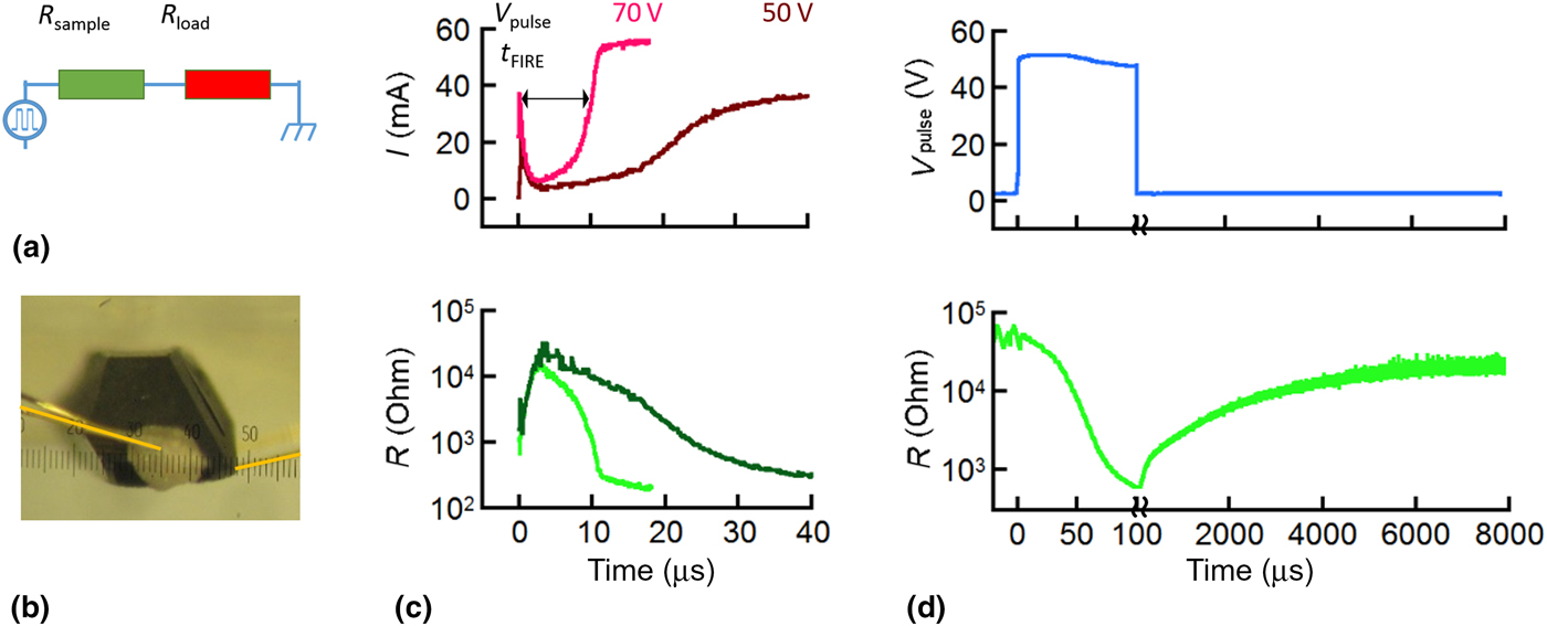
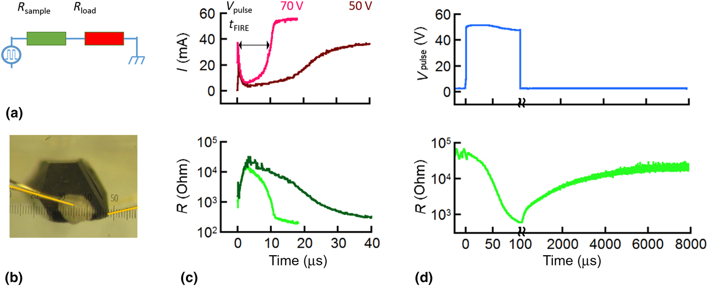
Electric Mott transition refers to the collapse of the Mott insulating state at the local scale when a Mott insulator is subjected to an electric field exceeding a threshold value. Previous studies have demonstrated that this phenomenon originates from an electronic avalanche breakdown which results in the creation of conductive filaments.[Reference Guiot, Cario, Janod, Corraze, Ta Phuoc, Rozenberg, Stoliar, Cren and Roditchev21] Electric Mott transition was reported in numerous narrow gap Mott Insulators[Reference Guiot, Cario, Janod, Corraze, Ta Phuoc, Rozenberg, Stoliar, Cren and Roditchev21–Reference Janod, Tranchant, Corraze, Querré, Stoliar, Rozenberg, Cren, Roditchev, Phuoc, Besland and Cario24] such as the lacunar spinel compounds GaM 4Q 8 (M = V, Nb, Ta, Mo; Q = S, Se),[Reference Cario, Vaju, Corraze, Guiot and Janod25] the canonical system (V1−xCrx)2O3[Reference Querré, Tranchant, Corraze, Cordier, Bouquet, Députier, Guilloux-Viry, Besland, Janod and Cario20, Reference Janod, Tranchant, Corraze, Querré, Stoliar, Rozenberg, Cren, Roditchev, Phuoc, Besland and Cario24] or the molecular Mott insulators [Au(Et-thiazdt)2].[Reference Stoliar, Diener, Tranchant, Corraze, Brière, Ta-Phuoc, Bellec, Fourmigué, Lorcy, Janod and Cario26] In this broad class of compounds, the most prominent signature of the electric Mott transition is the volatile resistance drop, also called resistive switching, that occurs under an electric field.[Reference Stoliar, Cario, Janod, Corraze, Guillot-Deudon, Salmon-Bourmand, Guiot, Tranchant and Rozenberg23, Reference Cario, Vaju, Corraze, Guiot and Janod25, Reference Stoliar, Diener, Tranchant, Corraze, Brière, Ta-Phuoc, Bellec, Fourmigué, Lorcy, Janod and Cario26] Figure 1 displays a typical resistive switching observed on a (V0.89C0.11)2O3 crystal at 164 K when voltage pulses are applied to the circuit made of the crystal in series with a load resistance. Each voltage pulse exceeding the threshold value (of the order of a few kV/cm) induces a volatile resistive switching and a burst of current into the circuit called firing event [see Fig. 1(c)]. The delay time before the firing event is called t FIRE and decreases with a higher applied voltage [~10 and 23 µs for 70 V (pink) and 50 V (dark red) applied pulses, respectively]. Figure 1(d) confirms moreover that the resistive switching is volatile as the resistance relaxes exponentially in time up to its initial value after the voltage pulse.
Experimental resistive switching measured for a (V0.89C0.11)2O3 crystal. (a) Experimental setup used for the experiments. (b) Picture of a (V0.89C0.11)2O3 crystal contacted with two gold electrodes highlighted by the yellow lines. (c) Volatile resistive switching (in green) concomitant with a burst of current (in red) observed when a voltage pulse is applied on the setup realized with a (V0.89C0.11)2O3 crystal in series with a 5 kΩ load resistor at 164 K. Two different voltages are applied. The resistive switching appears after a time t FIRE = 10 µs when a voltage pulse of V pulse = 70 V is applied (pink curve) and after t FIRE = 23 µs when V pulse = 50 V is applied (dark red curve). (d) Evolution of the resistance during and after the pulse. During the pulse, after the t FIRE, the resistance switches to the low resistive state. After the pulse, the resistance relaxes back up to its initial value.
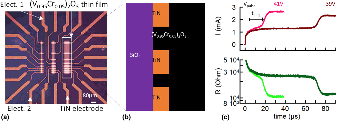
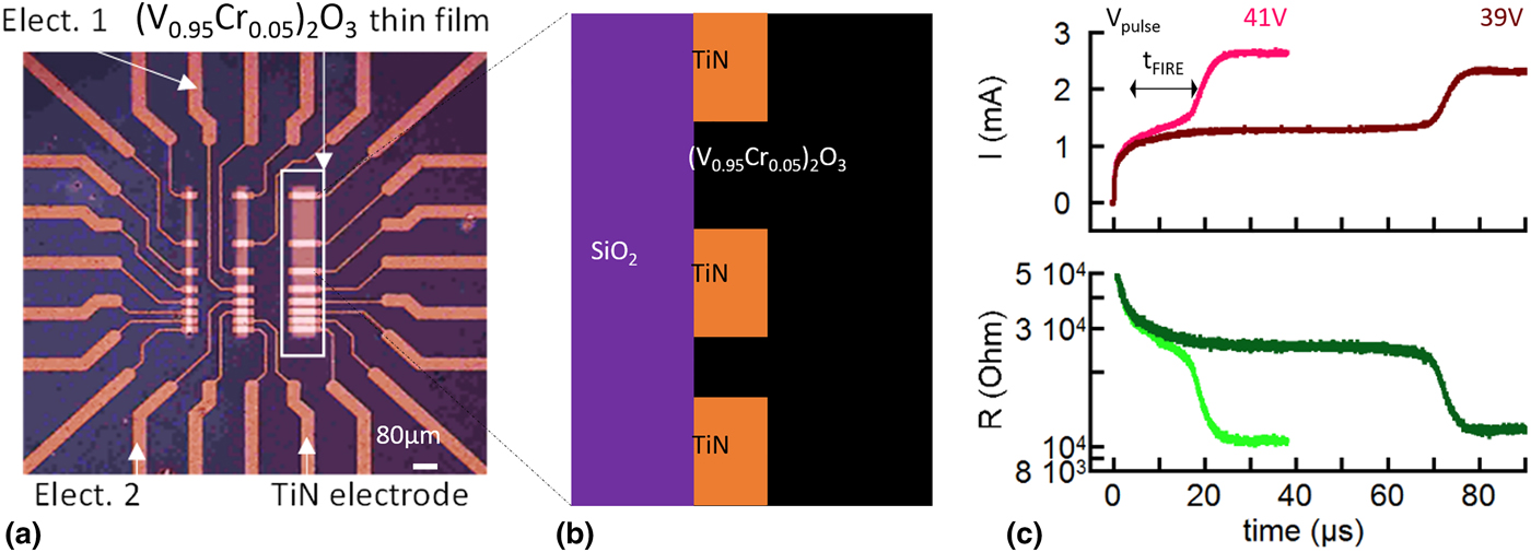
Recently, it was proposed that this resistive switching could be of interest for neuromorphic applications.[Reference Stoliar, Tranchant, Corraze, Janod, Besland, Tesler, Rozenberg and Cario18] But so far, this volatile resistive switching was only observed in Mott insulator in the form of crystals while its use in today's electronics necessarily implies its observation on thin-film devices. To tackle this issue (V0.95Cr0.05)2O3 polycrystalline thin films were prepared and characterized as detailed in the method section. Planar devices based on 1μm thick thin films and 160 to 2 µm inter-electrode distances were subsequently prepared to perform electrical measurements (see Fig. 2). Voltage pulses were applied at 185 K to the 20 µm inter-electrode devices thanks to a similar circuit as depicted in Fig. 1(a). The results of these experiments are displayed in Fig. 2(c) and demonstrate clearly that the planar device based on polycrystalline (V0.95Cr0.05)2O3 thin film exhibits a volatile resistive switching. As for the crystal, the resistive switching in thin films shows a variation of t FIRE with the applied voltage. This first demonstration of resistive switching in devices based on thin films of the Mott insulator (V0.95Cr0.05)2O3, opens, therefore, the possibility of using this new physical phenomenon in microelectronic applications such as neuromorphic component.[Reference Janod, Tranchant, Corraze, Querré, Stoliar, Rozenberg, Cren, Roditchev, Phuoc, Besland and Cario24] In particular, as described below the nonlinear electrical behavior of these devices might be taken into account to realize an artificial LIF neuron.
Resistive switching in (V1−xCx)2O3 planar thin-film device. (a) Picture of a (V0.95C0.05)2O3 planar device. The device is composed of three bands of the thin film with a various width (80, 40, and 20 µm) and various inter-electrodes distances (2, 3, 5, 20, 40, 80, and 160 µm). (b) Schematic cross-sectional view of the device along the large side of the white rectangle in (a). (c) Volatile resistive switching observed on a planar device at 185 K. Two different voltages are applied. At V pulse = 41 V, the resistive switching appears after the t FIRE = 20 µs and at V pulse = 39 V, the resistive switching appears after the t FIRE = 73 µs.
Toward a LIF artificial neuron made from (V0.95Cr0.05)2O3 thin films
In the mammal brain, neurons ensure three main functions that are called Leaky, Integrate, and Fire. The neurons are subjected to electric pulses coming from other neurons and they are integrating this signal through their membrane potential. Between pulses, the membrane potential relaxes and this feature is called “Leaky”. When the membrane potential reaches a certain threshold, then the neuron delivers an action potential toward other neurons and this event is called “Fire”. Lapicque was the first to notice that the neuron behavior before the Fire event was equivalent to the charge/discharge of a RC circuit. His model, called LIF model, aims therefore at describing the accumulation of electric charges through the cellular membrane of the neuron by representing the membrane as a capacitor with a leaking resistor in parallel.[Reference Brunel and van Rossum27, Reference Lapicque28] According to Lapicque, spikes arriving from other neurons inject electrical charges into the capacitor. When the membrane potential reaches a given threshold the neuron fires an output electric spike.
It was recently proposed that Mott insulator crystals reproduce the LIF behavior when they are subjected to electric pulses.[Reference Stoliar, Tranchant, Corraze, Janod, Besland, Tesler, Rozenberg and Cario18] As this behavior was never demonstrated on thin films that are more suitable for the realization of LIF artificial neuron we have explored the behavior of (V0.95Cr0.05)2O3 thin-film devices under train of pulses.
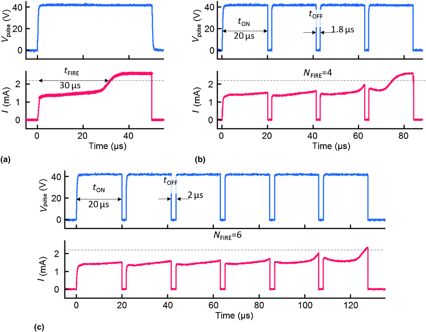
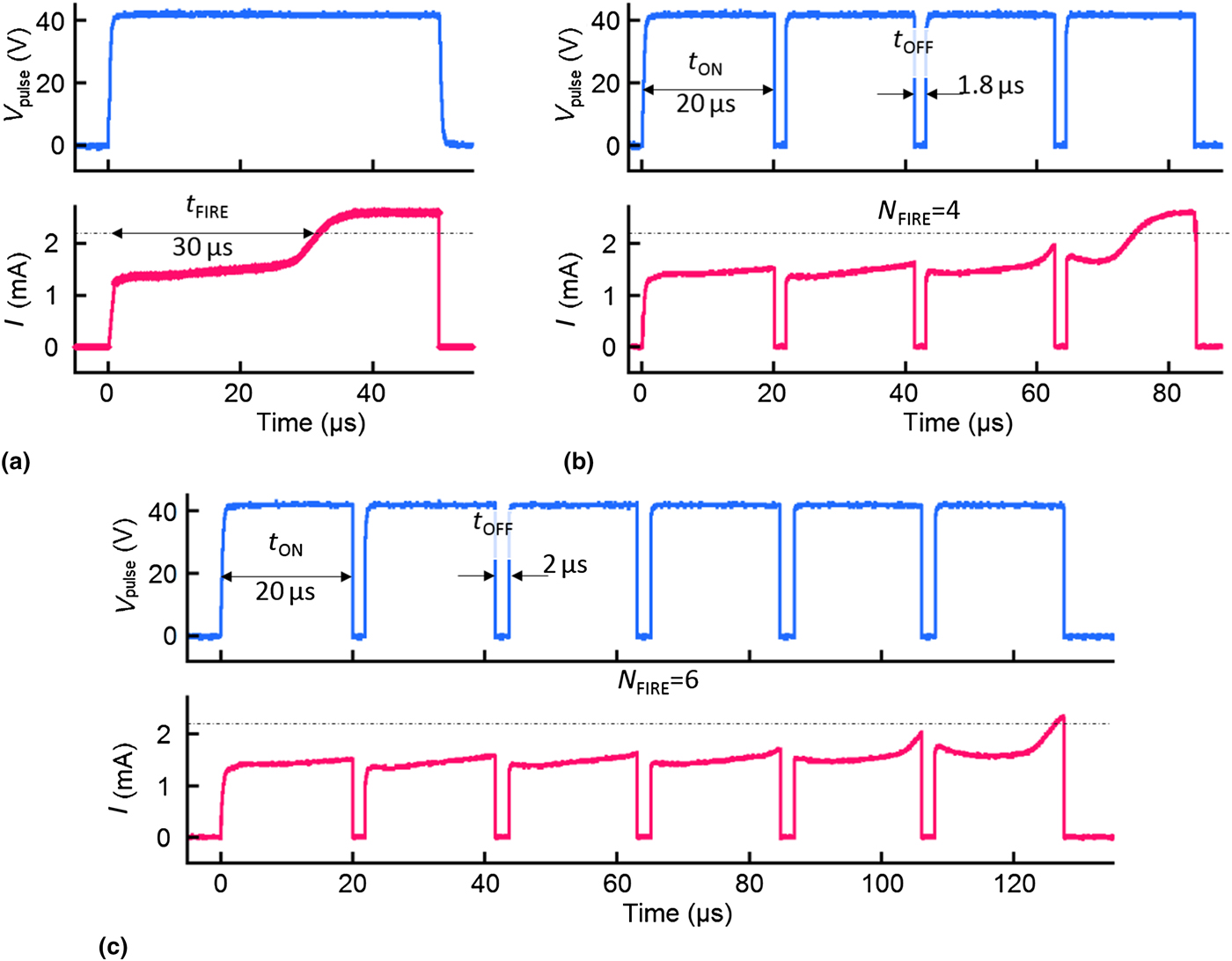
As shown in Fig. 3, when the (V0.95Cr0.05)2O3 thin-film device receives a single pulse of 50 µs duration, it undergoes a volatile resistive switching with t FIRE≈ 30 µs. A train of pulses of same voltage was subsequently applied to the device. All pulses in the train have a duration of t ON = 20 µs (i.e. duration shorter than t FIRE) and are separated by a time interval t OFF of the order of 2 µs. Obviously, without integration effect, no resistive switching should occur as t ON is shorter than t FIRE. But Fig. 3(b) reveals that with t ON = 20 µs (i.e. <t FIRE) and a time interval t OFF = 1.8 µs, a resistive switching appears during the fourth pulse. This experiment clearly demonstrates a cumulative effect (Integrate functionality) and shows that this integration is not perfect as the FIRE event occurs after a cumulated time close to 65 µs which is two times higher than t FIRE≈ 30 µs observed for the single pulse. This is further confirmed by increasing the time interval between two pulses from t OFF = 1.8 µs to t OFF = 2 µs, thus giving more time for relaxation. In this case, the number of pulses required to reach the firing event increases from 4 to 6. These experiments demonstrate therefore that simple planar devices based on polycrystalline (V0.95Cr0.05)2O3 thin films exhibit a LIF behavior that makes them suitable for the realization of a monocomponent artificial neuron.
Demonstration of the Leaky Integrate and Fire behavior on a (V0.95C0.05)2O3 planar thin-film device at 185 K. (a) Single pulse of 42 V applied on the device. The firing event appears after a t FIRE of 30 µs. The dotted line highlights the current threshold corresponding to the firing event. The current threshold is determined by the change of curvature during the volatile switching. (b), (c) Train of pulses (duration t ON) separated by a time interval t OFF. The dotted lines highlight the current corresponding to the firing event. (b) With t ON = 20 µs and t OFF = 1.8 µs, four pulses are necessary to induce the firing event (N FIRE = 4). (c) Increasing t OFF to 2 µs leads to an increase of N FIRE to 6. During the sixth pulse, the firing event is not completed but has begun, the current being above the dotted line.
Toward a predictive LIF model for Mott insulators
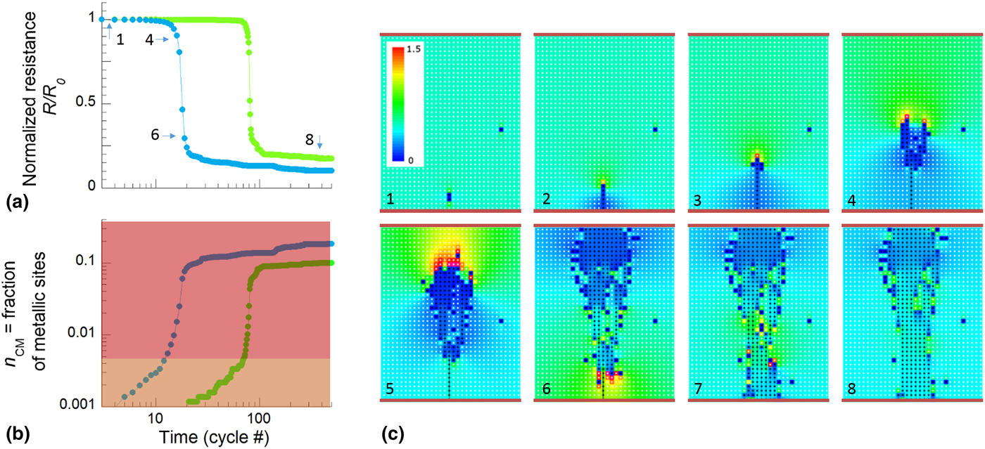
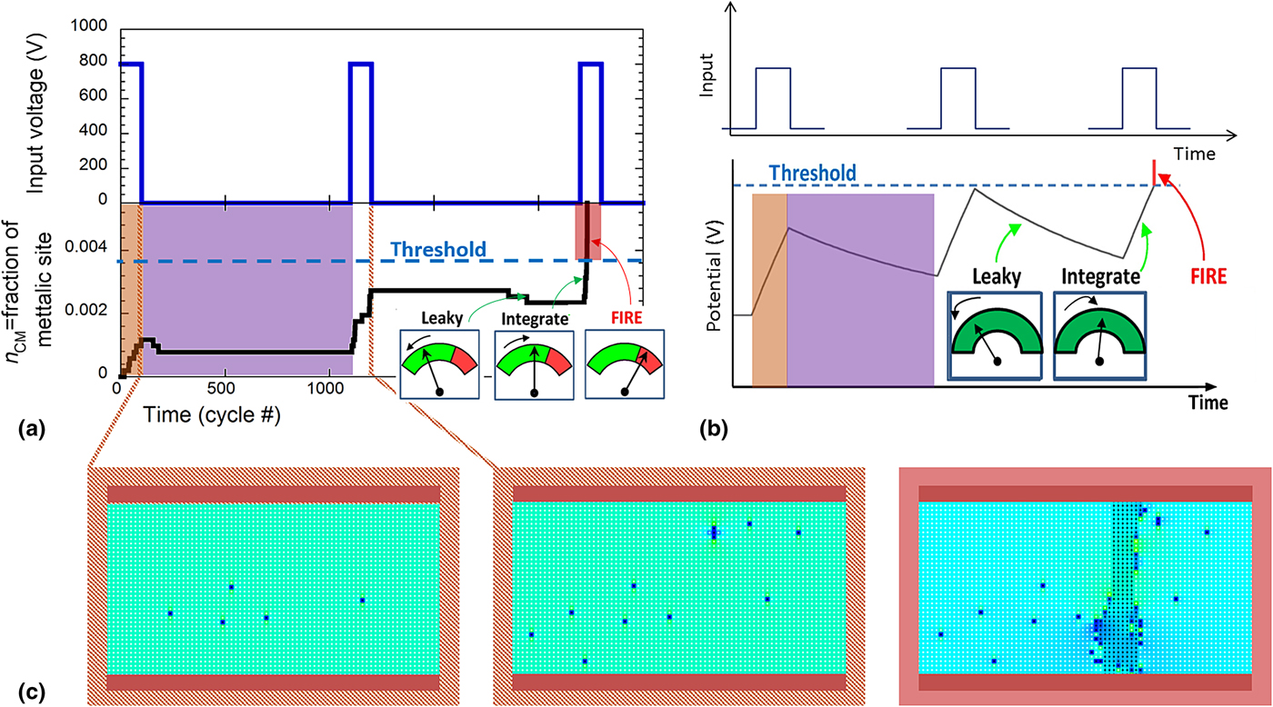
To reach a better comprehension of the resistive switching in Mott insulators a modeling work was engaged using a 2D (two-dimensional) resistor network. The method and the main results of this work were published elsewhere.[Reference Stoliar, Cario, Janod, Corraze, Guillot-Deudon, Salmon-Bourmand, Guiot, Tranchant and Rozenberg23, Reference Stoliar, Rozenberg, Janod, Corraze, Tranchant and Cario29] This resistor network implements an energy landscape between the most stable Mott insulating phase and the metastable correlated metallic phase. The probability of transition from the Mott insulating phase to the correlated metallic phase depends on the applied voltage while the probability of the transition back is a thermal activation process over a fixed energy barrier. This modeling work shows that a volatile resistance drop is obtained thanks to the apparition of the metallic filamentary path between the electrodes. Figures 4(a) and 4(b) display the dynamics of the creation (and relaxation) of metallic sites. At the beginning of the pulse, all sites are in the insulating state but under electric field, some insulating sites switch into metallic sites. During the pulse, the production rate of metallic sites largely overcome their relaxation rate; thus, the fraction of metallic sites increases up to a critical threshold above which a metallic filamentary path suddenly grows across the sample, bridging the two electrodes.[Reference Stoliar, Cario, Janod, Corraze, Guillot-Deudon, Salmon-Bourmand, Guiot, Tranchant and Rozenberg23, Reference Vaju, Cario, Corraze, Janod, Dubost, Cren, Roditchev, Braithwaite and Chauvet30] This process is illustrated in Fig. 4(c).
Modeling the behavior of a Mott insulator under electric field (a) Resistive switching observed after a delay time decreasing with the applied voltage. This applied voltage is higher for the blue curve than for the red one.[Reference Tranchant, Janod, Corraze, Stoliar, Rozenberg, Besland and Cario31] (b) Concomitant increase of the fraction of metallic sites in the resistor network. The orange area corresponds to the increase of metallic cells before the creation of the filamentary percolating path (threshold value is ~0.00375). The red area corresponds to the increase of metallic cell number during and after the creation of this filament. (c) Resistor network evolution as a function of time showing the filament formation. The red lines at the top and the bottom stand for the electrodes where the voltage is applied. The local electric field is represented by the color scale in snapshot 1: from zero in dark blue color to red in the higher. Time of snapshot 1, 4, 6, and 8 are indicated in (a).

To further understand the LIF behavior observed in the (V0.95Cr0.05)2O3 thin-film device, the modeling of a train of pulses shorter than the tFIRE was investigated. Figure 5(a) illustrates the behavior of the model displaying a resistive switching event during the third pulse of the train. Snapshots of the resistor network are presented in Fig. 5(c) at the end of each pulse. During each pulse, the fraction of metallic sites increases (dark blue), but there is also some relaxation of metallic sites back to the Mott insulating phase in between the pulses. If the time during pulses is not very long, the relaxation is not strong enough to completely relax back all metallic sites. Therefore the fraction of metallic sites increases with each successive pulse. As the fraction of metallic sites reaches a threshold value a filamentary percolating filament suddenly grows between the two electrodes.
Leaky Integrate and Fire (LIF) model. (a) Train of three pulses shorter than the t FIRE simulated on the resistor network. The orange, purple, and red areas correspond respectively to the Integrate (increase of the fraction of metallic sites), Leaky (decrease of the fraction of metallic sites) and Fire (the fraction of metallic sites exceeds the threshold) functions. (b) LIF model on RC circuit according to Lapicque. The orange and purple areas correspond respectively, to the Integrate (increase of the number of charges in the capacitor), Leaky (decrease of the number of charges in the capacitor) functions. Although postulated, the Fire function cannot be achieved with a simple RC circuit. (c) Simulated resistor network at the end of each pulse associated with (a).The number of the metallic site increases at each pulse. The red resistor network corresponds to the third pulse, where the fraction of metallic sites exceeds the threshold number, and a percolating filamentary path is created.

This modeling work suggests an interesting analogy, namely, that the accumulation of metallic domains in Mott insulators under electric field plays a similar role as the accumulation of charges on the membrane of biologic neurons. In fact, a more detailed analysis of the model described in Ref. [Reference Stoliar, Tranchant, Corraze, Janod, Besland, Tesler, Rozenberg and Cario18] demonstrates that the accumulation of metallic sites in Mott insulators follows the same dynamics, as the accumulation of charges in the LIF artificial neurons model. As a consequence, Mott insulators devices made either of crystals or polycrystalline thin films can be considered as a faithful realization of LIF artificial neurons.
Conclusion
Thin-film devices of the paradigmatic strongly correlated Mott insulator oxide (V0.95Cr0.05)2O3 were prepared by magnetron sputtering techniques. Volatile resistive switching similar to that observed on crystals were evidenced for the first time on these (V0.95Cr0.05)2O3 polycrystalline thin films while subjected to the electric field. This behavior may be explained thanks to a model of electric Mott transition showing the breakdown of the Mott insulating state at the local scale under an electric field. Moreover, the (V0.95Cr0.05)2O3 thin-film devices exhibit a significant LIF behavior under a train of electric pulses which is expected within the framework of this model. As a consequence, this work strongly suggests that downscalable LIF artificial neurons could be easily realized from two-terminal devices based on Mott insulator thin films. Such results appear as a crucial achievement toward the realization of on-chip Mott artificial neurons compatible with standard microelectronics.
Acknowledgments
The authors thank the “Région Pays de la Loire” for funding the present work in the framework of the “Pari scientifique Neuro-Mott”. P. S. acknowledges the support of the Spanish Ministry of Economy through the Ramón y Cajal (grant no. RYC-2012-01031).