In spite of high expectations and research effort during the past decade or so, carbon nanotube (CNT) transistor is still far from practical realization.[Reference Tans, Verschueren and Dekker1–Reference Franklin and Chen4] The key obstacle to harnessing the full potential of CNTs as the next-generation field-effect transistor (FET) channel materials lies in the contacts between CNTs and metal electrodes.[Reference Svensson and Campbell5] Unlike conventional FETs, CNT transistors function as Schottky barrier transistors, i.e., transistor action occurs by varying contact resistances.[Reference Heinze, Tersoff, Martel, Derycke, Appenzeller and Avouris6] However, fundamental understanding of the Schottky barrier formation and thus a guideline of atomic scale control of metal–CNT contacts are still lacking.[Reference Svensson and Campbell5, Reference Vitale, Curioni and Andreoni7] Whereas experimentalists have still made significant progress by employing an empirically optimized approach (e.g., Pd electrodes that wet CNTs well),[Reference Javey, Guo, Wang, Lundstrom and Dai3, Reference Franklin and Chen4, Reference Zhang, Franklin, Chen and Dai8] the situation is clearly undesirable for the future scientific and technological advances.
In this letter, by carrying out extensive large-scale first-principles calculations on a series of atomic metal–CNT junction models based on capped CNTs, we study the correlation between metal–CNT contact atomic structures and junction resistances and find the surprising effect of creating topological defects at metal–CNT contact regions in eliminating Schottky barriers. Previously, using conventional open-ended CNTs with and without hydrogen termination, we have established the significant effects of CNT diameter[Reference Kim and Byun9] and edge atomic structures and associated edge localized states on metal-induced gap states (MIGS) and Schottky barriers.[Reference Kim and Kim10] We especially confirmed that, if the resistance length scaling and the long-length-limit resistance are properly observed, these conventional junction models support the “stronger metal–CNT bonds → lower resistance” picture. However, we here demonstrate that novel atomistic junction models based on CNT caps can in fact achieve much lower contact resistance in spite of their weak metal–CNT bonds. It will be shown that the significant improvement in contact resistances is an intrinsic and general behavior of topological defects that preserve the sp 2 carbon network and form anomalous propagating-type hybrid gap states. We will further show that different arrangements of pentagon defects can result in significant variation in the conductance magnitude as well as the device polarity. This suggests that controlled defect nanoengineering will be a viable route toward reliable high-performance CNT device applications, enabling us to not only significantly improve the contact properties but also control the device functionality.
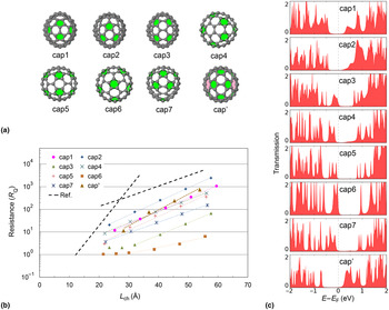
In Fig. 1(a), we first summarize the capped (10,0) CNT models employed in this work (details can be found in Fig. S1 of Supplemental Material). To create carbon caps, six pentagons must be introduced to a hexagonal bonding network according to Euler's theorem. For the (10,0) CNT, seven configurations are available to construct the cap while obeying the isolated pentagon rule (cap1–cap7).[Reference Brinkmann, Fowler, Manolopoulos and Palser11–Reference Khazaei, Dean, Farajian and Kawazoe13] The CNT caps, for example, play a crucial role in the CNT growth by determining the CNT chirality and diameter,[Reference Reich, Li and Robertson12] but they should be considered in this work as a source of topological defects within the carbon lattice at the CNT–metal contacts. We further note that, whereas the atomic structure and relative stability of different CNT cap models[Reference Brinkmann, Fowler, Manolopoulos and Palser11, Reference Reich, Li and Robertson12] and their possible role in field-emission applications[Reference Khazaei, Dean, Farajian and Kawazoe13] were previously discussed, their contact resistance to our knowledge has not been analyzed. To confirm the generality in terms of topological defect types, we additionally considered a rather artificial cap model constructed by starting from cap1 and introducing two heptagon defects next to two pentagon defects thus forming two pentagon–heptagon defects (cap').
(a) Top views of eight capped (10,0) CNT models employed in this work. Pentagon/hexagon topological defects are highlighted in green/pink. (b) Length scaling of contact resistances shown in the logarithmic scale. For comparison, resistance length scaling of a comparative open-ended (10,0) CNT model is also schematically shown (long dashed lines). (c) Transmission spectra of capped CNT junction models.

The device models were finalized by sandwiching the capped CNTs between two-layer 6 × 6 Al(111) slabs. The Al–CNT contact distance was fixed at 2.5 Å for a straightforward comparison of the charge injection capacity of different CNT models without the complication of the contact–distance dependence. Results at the optimal contact distances (between 2.5 and 3.3 Å, see Fig. S2 in Supplemental Material) do not modify the conclusions qualitatively (see Fig. S3 in Supplemental Material). In constructing the CNT and CNT-based junction models, we enforced mirror symmetry in order to avoid any ambiguity in the subsequent analysis resulting from differences in the two CNT cap and CNT–metal interface geometries. We note that such geometrical variations, e.g., the rotation of one cap atomic structure with respect to the other cap by 90°, do not qualitatively change our results (see Fig. S4 in Supplemental Material).
Two comments are worth making on our device models: The end-bonded geometry we adopt here, while it is often employed for the first-principles study of metal–CNT contacts[Reference Svensson and Campbell5] and allows one to check the resistance length scaling within first-principles calculations,[Reference Kim and Kim10] does not include side-bonding or wrapping electrode metal atoms that are more prevalently found in experiments. However, extending the end-bonded geometry to the embedded one by introducing additional side-bonded metal atoms within the allowed size in first-principles calculations only insignificantly modifies the junction transmission,[Reference Palacios, Tarakeshwar and Kim14, Reference Adessi, Avriller, Blase, Bournel, d'Honincthun, Dollfus, Fregonese, Galdin-Retailleau, Lopez-Bezanilla, Maneux, Nguyen, Querlioz, Roche, Triozon and Zimmer15] which indicates that the resistances across CNT ends are lower than those across CNT sides. Indeed, there exist experimental evidences that CNT edges are more preferable charge injection paths than CNT sides.[Reference Mann, Javey, Kong, Wang and Dai16, Reference Nosho, Ohno, Kishimoto and Mizutani17] This might explain why a recent experiment that included only side-bonding metal atoms found that, in contradiction to previous studies, the CNT device performance depends significantly on contact length.[Reference Franklin and Chen4] Next, because we use idealized contact geometry and a rather poor CNT electrode metal species,[Reference Zhang, Franklin, Chen and Dai8] Al, our results should represent the upper limit of contact resistance. The incorporation of metal species with a better wettability[Reference Vitale, Curioni and Andreoni7, Reference Zhang, Franklin, Chen and Dai8] and/or full relaxation of more realistic contact geometries in the embedded configuration[Reference Palacios, Tarakeshwar and Kim14, Reference Adessi, Avriller, Blase, Bournel, d'Honincthun, Dollfus, Fregonese, Galdin-Retailleau, Lopez-Bezanilla, Maneux, Nguyen, Querlioz, Roche, Triozon and Zimmer15] should strengthen the conclusions presented below.
We applied a first-principles approach based on density-functional theory (DFT) and matrix Green's function (MGF) calculations.[Reference Kim and Byun9, Reference Kim, Tahir-Kheli, Schultz and Goddard18] Density functional calculations within the PBE generalized-gradient approximation[Reference Perdew, Burke and Ernzerhof19] were carried out using the SeqQuest program (Sandia National Laboratories), which is based on norm-conserving pseudopotentials and Gaussian basis sets.[20] To extract the electronic and charge transport characteristics of junctions, we employed our in-house code that implements the MGF approach.[Reference Kim and Byun9, Reference Kim, Tahir-Kheli, Schultz and Goddard18, Reference Datta21] Starting from the DFT calculations for a deviced model and two separate bulk electrode models from which we extract surface Green's functions, we calculated spectral function, A(E) = i[G(E) − G+(E)], and transmission function, T(E) = Tr[Γ1 (E)G(E)Γ2 (E)G+(E)], where G and Γ are the retarded Green's function, G(E) = (ES − H + ∑1 + ∑2 )−1, and broadening matrix, Γ1,2 = i(∑1,2 − ∑1,2+), respectively. The self-energies ∑1/2 provide the ab initio broadening and shift of the channel energy levels attributed to the coupling between CNTs and metal electrodes 1/2.
In Fig. 1(b), we show the length scaling of resistances of capped CNT models, respectively, calculated using the Landauer formula[Reference Datta21]
 $$R=\displaystyle{h \over {2{\rm e}^2 }}\displaystyle{1 \over {T\lpar E_{\rm F} \rpar }}=R_{\rm Q}+\displaystyle{h \over {2{\rm e}^2 }}\displaystyle{{1 - T\lpar E_{\rm F} \rpar /M} \over {T\lpar E_{\rm F} \rpar /M}}\comma \;$$
where h is the Planck's constant, T(E F) is the transmission at the Fermi level, E F, M is the number of modes (2 for CNT), and R Q = h/4e2 ≈ 6.5 kΩ is the quantized minimum contact resistance. Transmission spectra of all capped CNT models with L ch ≈ 4.5 nm are summarized in Fig. 1(c). For our short ballistic CNT models, the resistance follows the expression for the tunneling in metal–insulator–metal junctions and scale exponentially with channel length L ch as
 $$R=R_0 \exp \lpar \beta L_{{\rm ch}} \rpar \comma \;$$
where R 0 is an effective contact resistance and β is the tunneling growth constant,[Reference Simmons22] with a minimum resistance of R Q. We have recently demonstrated that the resistance length scaling of usual metal–CNT contact models changes from the short-length large-β Schottky-barrier-dominated regime to the long-length small-β CNT-intrinsic regime.[Reference Kim and Kim10] The transition length or twice Schottky barrier width was found to sensitively depend on the atomistic details of metal–CNT contacts. In Fig. 1(b), as a reference, we reproduce the schematic length scaling obtained for the (10,0) CNT without H passivation, which showed a significantly better charge injection capacity than its hydrogenated counterpart.[Reference Kim and Kim10]
Now, focusing on our novel capped CNT models, we find that the contact resistance of capped CNTs is smaller than that of uncapped CNTs by up to a factor of 103. Taking into account their weak metal–CNT chemical bonds (binding energies of <0.1 eV; see Fig. S2), this establishes that rather than the strong metal–CNT bonds the preservation of sp 2 character across metal–CNT contacts is the key design parameter for optimal device performance. Especially, we find only single CNT-body-dominated low-slope length scaling behavior for all capped CNT models (with β ranging from 0.065 to 0.139). The absence of Schottky-barrier-determined high-slope length scaling at short L ch indicates that the low resistance is an “intrinsic” property of capped CNT models. Moreover, the similar behavior of the cap' model with two pentagon–heptagon defects (rather than pentagon defects) indicates that the improved contact properties is a “general” characteristic of topological defects embedded into the CNT wall [see Fig. 1(a) and Fig. S1].
Irrespective of the qualitatively similar Schottky-barrier-absent length scaling behavior and generally better charge injection capacity of all capped CNT models than their conventional counterparts such as hydrogenated or dehydrogenated open-ended CNTs,[Reference Kim and Kim10] we find in Fig. 1(b) that the resistance values of the capped CNTs span several orders of magnitude (between 41 kΩ for cap3 and 16 MΩ for cap2 at L ch ≈ 6 nm). Moreover, as shown in Fig. 1(c), we find that the device type of capped CNT models is not unique: the fullerene-like distribution of pentagons and hexagons (existence of only the pyracylene-like arrangement of pentagons and hexagons) endows cap1 and cap2 models as well as cap' based on cap1 with the n-type conductivity, while the other cap models show the p-type conductivity. It should be noted that all our CNT models are undoped and the p- or n-type device characteristics result from the orbital hybridization and corresponding charge transfer at metal–CNT interfaces discussed below.
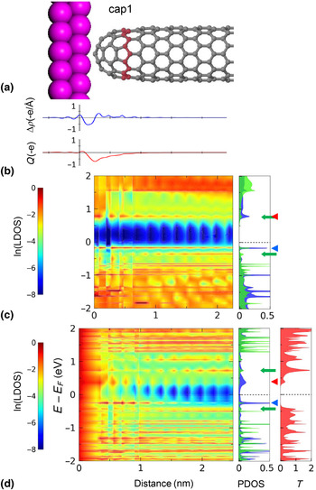
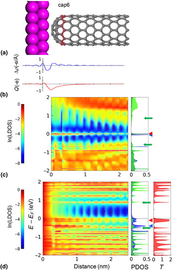
Using the cap1 and cap6 junction models with lengths of about 5.5 nm shown in Figs. 2(a) and 3(a), respectively, we next extract the microscopic origin of the intrinsically low-resistance contacts based on topological defects as well as the quantitative differences in resistance values [Fig. 1(b)] and device polarities [Fig. 1(c)]. Characterizations of higher-resistance n-type cap1 (lower-resistance p-type cap6) presented below can be similarly applied to, e.g., cap2 (cap3). First, we observe the plane-averaged real-space charge redistributions at the metal–CNT contacts Δ ρ = ρ CNT + Al − (ρ CNT + ρ Al) and integrated plane-averaged charge density differences Q(z) = ∫0z Δ ρ(z ′)dz ′ shown in Figs. 2(b) and 3(b). A positive (negative) Δ ρ indicates a gain (loss) in electron density upon the metal–CNT coupling, while a positive (negative) Q indicates a right-to-left (left-to-right) electron transfer. We find that the induced charge redistribution patterns in both cap models are, except for the slightly larger charge transfer in cap6, very similar and characterized by a strong “push-back effect” originating from Pauli repulsion. Whereas the pushed-back electrons rapidly attenuate along the Al side, a significantly long-ranged net charge transfer is induced along the CNT direction. All capped CNT models in fact show similar charge transfer properties (Fig. S5 in Supplemental Material).
Structural, electrostatic, electronic, and transport properties of cap1 and Al(111)-cap1 contacts. (a) Side view of the junction model. The corresponding (b) plane-averaged charge density differences at the Al–CNT interface and its integration, and LDOS along the channel for the CNT (c) without and (d) with electrodes. For both LDOS plots (c) and (d), corresponding PDOS of CNT cap (blue) and body (green) are shown together. For the metal–CNT composite model (d), transmission is also shown.

(a) Side view of the Al(111)-cap6 junction model. The corresponding (b) plane-averaged charge density differences at the Al–CNT interface and its integration, and LDOS along the channel for the CNT (c) without and (d) with electrodes. For both LDOS plots (c) and (d), corresponding PDOS of CNT cap (blue) and body (green) are shown together. For the metal–CNT composite model (d), transmission is also shown.

Because the electrostatic information cannot discriminate different capped CNT models, we next study the energy-level alignment and energy-dependent charge injection properties analyzed by the local density of states (LDOS), projected density of states (PDOS), and transmissions. We first consider LDOS and PDOS of cap1/cap6 without and with metal contacts shown in Fig. 2(c)/3(c) and Fig. 2(d)/3(d), respectively. Transmissions are also shown for the junction models in Figs. 2(d) and 3(d). In Figs. 2(c) and 3(c), the most noticeable features of isolated capped CNTs are the gap states peaked at the CNT caps and propagate into the CNT body (denoted by left red and blue triangles) that appear between bulk band edges (indicated by green left arrows). These states originate from the strong hybridization between pentagon defect states, the zigzag edge states, and the CNT body states. Apparently, their detailed characters including energetic location depend on the arrangement of pentagons.
Upon contacting the capped CNTs to metals and with the corresponding charge transfer, these hybrid states energetically shift and become “metal-induced” gap states as shown in Figs. 2(d) and 3(d) (denoted by red and blue triangles). As indicated by the large energetic shift and broadening, the charge transfer is largely accommodated by hybridized defect or gap states. Some of them (indicated by red left triangles) propagate deep into the CNT body to induce significant transmissions and determine device polarities, but the others (indicated by blue left) decay exponentially and induce negligible transmissions.
There are several points we need to emphasize. First, the LDOS and PDOS spectra shown in Figs. 2(c) and 3(c) were obtained for isolated semi-infinite capped CNTs using the MGF formalism. So, unlike DFT data (which should be computed for finite CNTs with an arbitrary broadening parameter), they faithfully show the connectivity between topological defect or zigzag edge states near CNT caps with semi-infinite CNT body states and enable us to understand why cap1 is a better metallic contact than cap6: Compared with the band edges of cap1 that clearly show the preserved identities of isolated cap or body states in LDOS [Fig. 2(c)] and corresponding identifiable PDOS peaks (green left arrows in PDOS), the band edges of cap6 are more strongly spatially delocalized and energetically broadened [Fig. 3(c)]. In addition, the gap states of cap6 are originally located at E F, so with the hybridization with metallic surface states they induce strong p-type transmission with noticeable Fermi-level contribution [Fig. 3(d)].
Second, in spite of these differences, it should be noted that all the capped CNT models are Schottky-barrier-free low-resistance contacts and show in LDOS a clear signal that evidences good metal–CNT electronic connectivity, namely continuous LDOS spectra in the metal–CNT cap interface regions [Figs. 2(d) and 3(d)]. This is in clear contrast with conventional models, e.g., open-ended CNTs, which showed distinctively disconnected LDOS at the metal–CNT interface region.[Reference Kim and Kim10] Although abnormal gap states that can couple with metallic states are available from localized zigzag CNT edge states,[Reference Nakada, Fujita, Dresselhaus and Dresselhaus23, Reference Kawai, Miyamoto, Sugino and Koga24] we found that they are intrinsically decoupled from CNT body states. So, upon contacting with metals, the MIGS originated from CNT edge states “exponentially decay” into the CNT body and give negligible transmission near E F. Stressing once more, we found an inherently different gap states with capped CNTs. The gap states originating from topological defect states that are well connected with CNT edge and body states induce unusual “propagating-type” MIGS [Figs. 2(d) and 3(d)], and they result in the intrinsically low resistance or the absence of Schottky-barrier-determined resistance length scaling [Fig. 1(b)].
We finally note that having both topological defect states and CNT body states (and the good coupling between them) is necessary to achieve such low-resistance contacts. In our previous study of polymerized C60 chains, in spite of the presence of topological defect states at the metal-wire contacts, the limited electronic connectivity between C60 units resulted in exponentially decaying MIGS and negligible T(E F).[Reference Lee, Kang and Kim25]
In summary, applying a first-principles computational approach to a series of junction models based on capped CNTs, we have established that, rather than strong chemical bonds, the preservation of sp 2 carbon network across metal–CNT contacts is the key requirement to achieve low junction resistances. More specifically, we showed that topological defects within the CNT caps form gap states that are well connected with the CNT body states, and, upon contacting with electrodes, result in propagating-type MIGS and intrinsically low-resistance metallic contacts. We further pointed out that the rational placement of topological defects can be a novel scheme to control device polarity.
Acknowledgments
This work was supported by the Korea Science and Engineering Foundation (KOSEF, Grant No. 2008-02807) funded by the Ministry of Education, Science and Technology. H.S. Kim, H.S. Kim, and Y.H. Kim were also supported by the National Research Foundation (NRF, Grant No. 2010-0006910). J.K. Kang and G.I. Lee were also supported by the WCU program (R-31-2008-000-10055-0) and the Korea Center for Artificial Photosynthesis (NRF-2009-C1AAA001-2009-0093879).
Supplementary materials
For supplementary material for this article, please visit http://dx.doi.org/10.1557/mrc.2012.14