Potential applications for flexible and stretchable electronic devices are very vast, ranging from electronic skin to health and wellness monitors. Conventional electronic devices based on stiff substrates are unable to fulfill these needs. Reference Honda, Harada, Arie, Akita and Takei1–Reference Kim, Xiao, Song, Huang and Rogers3 A basic building block of such devices is the flexible and stretchable electrode. Various strategies to lend stretchability to electrodes have been used, which include the use of networks of low-dimensional materials and the design of mechanically flexible and stretchable structures. Several groups have reported using networks of materials, such as carbon nanotubes, Reference Zhu and Xu4–Reference Kim, Song, Ha, Kim, Kim, Chung, Lee and Hong6 graphene, Reference Kim, Bae, Kim, Cheng, Kim, Kim, Li, Wu, Du, Kim, Kim, Estrada, Hong, Huang, Pop and Rogers7,Reference Kim, Zhao, Jang, Lee, Kim, Kim, Ahn, Kim, Choi and Hong8 silver nanowires, Reference Lee, Lee, Lee, Yeo, Hong, Nam, Lee, Lee and Ko9–Reference Ho, Cheng, Tey and Wei11 conductive polymers Reference Lipomi, Tee, Vosgueritchian and Bao12,Reference Lipomi, Lee, Vosgueritchian, Tee, Bolander and Bao13 or a mixture of them Reference Lee, Lee, Kim, Lee, Park, Choi, Kim, Kim, Lee, Nam and Park14 to form stretchable electrodes. Thin films of these materials maintain good electrical conductivity even upon mechanical deformation. On the other hand, other groups continue to use metal electrodes with high intrinsic electrical conductivity. By clever design of the metal electrodes, the maximum strain experienced by metal electrodes during flexing and stretching is minimized. Reference Chou, Lee and Kim15–Reference Robinson, Aziz, Liu, Suo and Lacour24 These structures are fabricated using conventional semiconductor processing techniques, such as photolithography, sputtering, evaporation and etching and often utilize the transfer printing method.
In this work, we explore the use of an alternative manufacturing method, screen printing, to fabricate stretchable metal electrodes. Screen printing, a low cost and large area printing method, is attractive for scalable commercial applications. However, the size of features printed using screen printing is larger than the size of features achievable via conventional semiconductor processing techniques. The relatively larger dimension of screen printed electrodes is undesirable because thinner films are less susceptible to fracture and more suitable for flexible and stretchable applications. Reference Romeo, Liu, Suo and Lacour25 Nonetheless, the simple manufacturing method used in this work can likely be used in low cost and large area applications which demand on the stretchability is lower.
Screen printing of stretchable electrodes was also examined by Someya et al. Reference Sekitani, Nakajima, Maeda, Fukushima, Aida, Hata and Someya26 An intrinsically stretchable conductor comprising of carbon nanotubes dispersed in a fluorinated rubber was formulated for screen printing. The achieved stretchability is beyond 100%. The relatively low electrical conductivity of the conductor developed (relative to conductivity of bulk silver ∼600,000 S/cm), 102 S/cm, may limit its use in large area applications where low series resistance is very crucial.
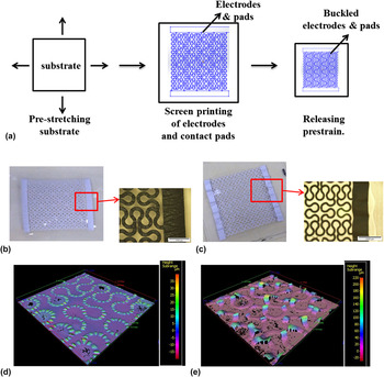
Figure 1(a) illustrates the steps in fabricating stretchable metal electrodes via screen printing. The stretchable silicone substrate (Bisco HT-6240, Rogers Corporation, CT) was prestretched 20% biaxially. While the substrate was still in its prestretched state, the silver paste (LS-411AW, Asahi Chemical Research, Tokyo, Japan) was screen printed onto the substrate using a stencil with serpentine designs. The substrate was pretreated using oxygen plasma when a good bond is desired between the substrate and the electrode. Plasma treatment is often performed to remove residual organic contaminants on a surface and improves wettability for better film adhesion to the substrate surface. Poor adhesion results in the absence of plasma treatment. However, even when the substrate was not oxygen plasma treated, the silver paste can be completely screen printed onto the substrate. As the bond between the substrate and electrode is weak, out-of-plane motion of the Ag electrode is possible. The screen printed Ag paste was cured at 150 °C for 30 minutes before the prestrain in the stretched silicone substrate was released. This eventually results in a buckled serpentine Ag electrode. The thickness and width of the printed Ag electrode are ∼19 and ∼200 µm, respectively. Parts b and c of Fig. 1 show the optical images of the buckled serpentine Ag electrodes formed when the Ag electrodes are well and poorly adhered to the substrate, respectively. Their 3D images are shown in Figs. 1(d) and 1(e), respectively. When there is good adhesion between the electrode and substrate, the amplitude of the buckled electrode is relatively small (∼20 µm), compared to the electrode with poor adhesion to the substrate (between 100 and 200 µm). As the prestrain applied to both samples is the same, the wave length (i.e., lateral distance between two neighboring peaks in the buckled electrode) of the buckled electrode with good adhesion to the substrate is smaller than that of the electrode with poor adhesion, to accommodate the similar magnitude of compressive stress set up after prestrain is released.
Stretchable electrodes. (a) Schematic illustration of the fabrication of stretchable electrodes. (b, c) Optical images of the printed electrodes. The electrodes are (b) well adhered and (c) poorly adhered to the substrate, respectively. The scale bars in the optical images are 1 mm. (d, e) 3D images of the electrodes measured using the focus-variation technique. The electrodes are (d) well and (e) poorly adhered to the substrate, respectively.

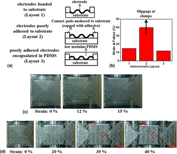
The Ag electrode poorly adhered to the substrate is not constrained by the substrate and is able to twist and bend when stretched to reduce the strain energy it experiences. This is expected to enhance its stretchability. However, such electrodes can be easily damaged by physical contact because they are exposed to the ambient conditions. Encapsulation is expected to circumvent this problem. Three various layouts of the electrodes are examined, as shown in Fig. 2(a). The first and second layouts are Ag electrodes which are well or poorly adhered to the substrate without encapsulation, respectively. The good adhesion between the electrode and substrate is achieved by performing oxygen plasma treatment to the substrate before printing the electrodes. In the absence of oxygen plasma pretreatment, the Ag electrode does not adhere well to the substrate. The last layout (layout 3) is Ag electrode which is poorly adhered to the substrate but encapsulated by polydimethylsiloxane (PDMS) with a modulus of 0.04 MPa, formed via mixing 50 parts of prepolymer and one part of curing agent.
Layout of the electrodes. (a) Three types of electrode layouts. From top to bottom: (1) electrodes are well bonded to the substrate, (2) electrodes without encapsulation are poorly adhered to the substrate and (3) electrodes, which are poorly adhered to the substrate, are encapsulated in low modulus PDMS. (b) Strain at which the electrodes fail (strain at failure) for the three different layouts of electrodes when the electrodes are stretched in the axis parallel to which the two contact pads lie along. Optical images of the electrodes with (c) layout 1 and (d) layout 2 at various levels of strain as the electrode is stretched along the axis that the 2 contact pads lie.

The three types of electrodes are stretched uniaxially and their specific strains at which the electrical resistance increases infinitely (i.e., strain at failure) are noted, as shown in Fig. 2(b). The electrodes with good adhesion to the substrate (layout 1) and the electrodes with poor adhesion to the substrate are encapsulated by low modulus PDMS (layout 3) fail consistently at 15 and 12% strain, respectively, regardless of whether the electrodes are stretched along the axis where the contact pads lie or perpendicular to the axis. On the other hand, the electrodes with poor adhesion to the substrate and are not encapsulated by low modulus PDMS (layout 2) exhibit higher strain at failure. When stretched to 40%, slippage starts to occur (due to the low clamping force of the stretch stage) but the electrodes still exhibit good conductivity. The stretchability of these electrodes is significantly lower than other works with electrodes of smaller thickness (several hundreds of nanometers) Reference Zhang, Xu, Fu, Lee, Su, Hwang, Rogers and Huang19,Reference Zhang, Wang, Li, Fan, Xu, Song, Choi, Yeo, Lee, Nazaar, Lu, Yin, Hwang, Rogers and Huang20 because the screen printed electrodes are ∼200 µm in width and ∼19 µm in thickness. During stretching, the electrodes bend and twist to reduce the strain energy in them. The torsion stiffness GJ T = wt 3/3, out-of-plane bending stiffness EI o = wt 3/12, and in-plane bending stiffness EI i = w 3 t/12 of structures are dependent on their thickness (t) and width (w). Hence, electrodes with larger thickness and width have lower ability to accommodate the strain energy during stretching and exhibit lower stretchability.
The electrode with good adhesion to the substrate (layout 1) is restricted to the substrate during stretching while the electrode with poor adhesion to the substrate (layout 2) can twist and bend out-of-plane of the substrate. Hence, electrode with layout 2 is able to accommodate the strain energy during stretching more effectively. Images of the 2 electrodes (layout 1 and 2) during stretching are shown in Figs. 2(c) and 2(d), respectively. Even though there is no visible fracture in the electrode with layout 1 [Fig. 2(c)], the electrode exhibits an infinite increase in electrical resistance when stretched to 15%. This is due to the formation of microcracks (See supplementary material (Figure 2) for scanning electron microscope images). The strain at the failure of the electrode is lower than 20% (the magnitude of the substrate prestrain) because the sites where buckles and wrinkles formed in the electrode are also dependent on where the release of substrate prestrain was initiated. Release of the substrate prestrain did not occur simultaneously across the substrate. The sites which experience largest strain during subsequent stretching may not correspond to the sites where the buckles and wrinkles are.
On the other hand, the electrode with layout 2 can be stretched to larger strain without failure. As the electrode is stretched along the axis which the contact pads lie along, the serpentine structures that run parallel to the axis are stretched and the structures that run perpendicular to it are compressed further out-of-plane (possible because of the poor adhesion to substrate) due to Poisson effect. At high strains, the stretched serpentine structures begin to tear near the points of highest curvature [circled in red in Fig. 2(d)] where the stress concentration occurs. Reference Kim, Liu, Kim, Wu, Song, Kim, Huang, Hwang, Zhang and Rogers18,Reference Zhang, Wang, Li, Fan, Xu, Song, Choi, Yeo, Lee, Nazaar, Lu, Yin, Hwang, Rogers and Huang20 At these sites, the strain has reached the fracture strain of the Ag, which results in its catastrophic failure. The loss in electrical conductivity, at this point, is not recoverable. This is unlike the case of the electrode with layout 1. As the failure of the electrode with layout 1 is due to the formation of microcracks, the gaps between the Ag particles in the electrode are closed up when the strain is released and the electrical conductivity recovers.
Finally, the strain at failure of the electrode with poor adhesion to the substrate and is encapsulated by low modulus PDMS (layout 3) is 12%, which is significantly lower than the electrode with layout 2. This implies that the PDMS encapsulation layer, despite its low modulus, impedes the motion of the electrode. In earlier works, it has been reported that an encapsulation layer of liquid medium does not significantly interfere with the electrode while the use of low modulus encapsulation layer still affects the mechanics of the stretched electrode. Reference Kim, Liu, Kim, Wu, Song, Kim, Huang, Hwang, Zhang and Rogers18,Reference Cheng, Zhang, Hwang, Rogers and Huang27 It can be expected that the use of a gaseous or liquid medium between the electrodes encapsulated by a thin and solid top elastomer layer minimizes the impedance of the motion of the electrode.
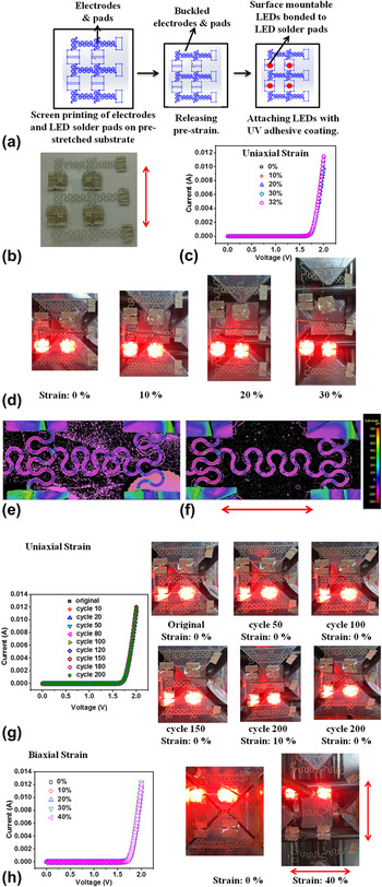
The electrodes with maximum stretchability (layout 2) are integrated with surface mounted light emitting diodes (LEDs) to demonstrate a stretchable LED matrix. The steps to fabricate a stretchable LED matrix are illustrated in Fig. 3(a). The Ag electrodes, LED solder pads, and contact pads were screen printed while the silicone substrate was in a biaxially prestrained state. After curing the screen printed Ag paste and releasing the prestrain in the substrate, the Ag electrodes and pads were buckled. The LEDs were subsequently bonded onto the LED solder pads using silver paste. A thin layer of acrylic based UV adhesive was coated over the LEDs to encapsulate them. An image of the completed LED matrix is shown in Fig. 3(b).
Stretchable LED matrix. (a) Schematic illustration of the fabrication of LED matrix with enhanced stretchability. (b) Optical image of the completed LED matrix. The electrodes between the LEDs are poorly adhered to the substrate [layout 2 of Fig. 2(a)]. The LED matrix can be stretched biaxially (in the axis indicated by the red arrow and in the axis perpendicular to it). (c) Current–voltage curves of the LED matrix from part (b) at various levels of system strain as the LED matrix is stretched along the axis of the red arrow shown in part (b). (d) Optical images of the LED matrix at various levels of system strain as the LED matrix is stretched along the axis of the red arrow shown in part (b). (e, f) 3D images of the LED matrix measured using the focus-variation technique. The LED matrix is at (e) 0% and (f) 34% uniaxial strain respectively. (g) Current–voltage curves of the LED matrix at different cycles of stretching to 10% strain and relaxing. The images on the right show the LED matrix after different number of cycles of stretching to 10% and relaxing. (h) Current–voltage curves of the LED matrix at various levels of system strain as the LED matrix is stretched biaxially (as indicated by the red arrows). Optical images of the LED matrix at 0 and 40% biaxial strain are provided on the right.

The LED matrix can be stretched both parallel and perpendicular to the axis along which the LED solder pads lie [i.e., the axis indicated by the red arrow in Fig. 3(b)]. The system strain at failure of the LED matrix (i.e., the strain at which any one of the LEDs is no longer illuminated) when stretched in the parallel or perpendicular axes are 30 ± 5 and 32 ± 7%, respectively. Figure 3(c) shows the current–voltage curves of the LED matrix when stretched to different extents in the axis parallel to which the LED solder pads lie. The current–voltage curves of the LED matrix hardly change as the LED matrix is stretched up to 32%. Images of the LED matrix as it is stretched up to 30% are shown in Fig. 3(d). The stiff LEDs encapsulated by UV adhesive (modulus: 8 MPa) maintain their dimensions during stretching. Only the electrodes connecting the LEDs are strained during stretching. More images of the LED matrix when stretched perpendicular to the axis along which the LED solder pads lie can be found in Supplementary Figure 4. In the case, when one of the LEDs is no longer illuminated, the cause of the failure can be traced to the fracture in the electrode leading to that LED. The fracture occurs close to the point of highest curvature and next to the LED, where the stress concentration is.
We also observe the evolution of the topography of the electrode connecting the LEDs as it is stretched using the focus-variation technique, as shown in parts e and f of Fig. 3. The LED matrix is stretched uniaxially at 0 and 34% in Figs. 3(e) and 3(f), respectively. As the sample is stretched uniaxially along the axis indicated by the red arrow at the bottom of Fig. 3(f), the length of the electrode lying along the strain axis increased by 34% while the electrode lying perpendicular to it decreased in length by 14.5%, indicating a Poisson's ratio of ∼0.43. The amplitude of the buckled electrodes decreases by less than 6%. On the other hand, the curvature of the serpentine electrodes lying parallel and perpendicular to the stretch axis has decreased and increased significantly, respectively. This implies that the strain during stretching is also accommodated by the bending of the electrodes, besides the “flattening” of the buckled electrodes.
The LED matrix is also repeatedly stretched to 10% and relaxed for 200 cycles. Figure 3(g) shows that the current–voltage curve stays similar even after the 200th cycle of stretching and relaxing. The images in Fig. 3(g) show the LED matrix after various numbers of cycles of stretching to 10% and relaxing. The electrodes and LEDs maintain their original layout after multiple cycles of stretching and relaxing.
When subjected to biaxial stretching, the LED matrix does not fail even beyond 40% strain (when slippage begins to occur at the clamps). Figure 3(h) shows the current–voltage curves of the LED matrix when stretched to different extents biaxially (along the axis parallel and perpendicular to which the LED solder pads lie). The current–voltage curve of the LED matrix remains unchanged as it is stretched up to 40%. The corresponding images of the LED matrix at 0 and 40% biaxial strain are also shown on the right of Fig. 3(h). During biaxial stretching, Poisson effect is absent and the sample does not contract in the axis perpendicular to the stretch axis, unlike in the case of uniaxial stretching. This eliminates failure via compressive strain of the electrodes that can occur when a uniaxial strain is applied, as shown in Supplementary Figure 4.
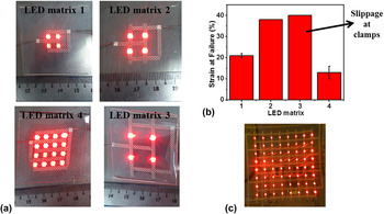
LED matrices with different areal coverage of LEDs are also investigated. Figure 4(a) shows the images of four different LED matrices. The first three matrices are 2 × 2 LED matrices with areal coverage of 18.5, 8.75, and 3.3% (clockwise from the top left). The last matrix is a 4 × 4 LED matrix with a fill factor of 18.5%. The printed areas range between ∼15 mm × 15 mm and ∼40 mm × 40 mm. The four types of LED matrices are stretched uniaxially and the system strain at which the electrical resistance increases infinitely (i.e., strain at failure) are noted, as shown in Fig. 4(b). The strain at failure of the four LED matrices, labeled 1 to 4 in Fig. 4(a), are 21 ± 1, 38, >40% (slippage at clamps when strained to 40%) and 13 ± 3%, respectively. As the areal coverage of the LEDs decreases, the stretchability increases because longer electrodes between the LEDs accommodate higher applied strain. However, the longer electrodes also increase the series resistance in the circuit. The relatively larger width and thickness of the electrodes formed via screen printing compensates this by decreasing the resistance. The stretchability of the 4 × 4 LED matrix is lower than the 2 × 2 LED matrix with a similar areal coverage. This could likely be due to the LED matrix with larger area being more likely to fail with more sites where stress concentration occurs. A large area (∼150 mm × 150 mm) 8 × 8 LED matrix is also demonstrated, as shown in Fig. 4(c).
Large area printable LED matrix with enhanced stretchability. (a) Optical images of 4 different LED matrices printed. Clockwise from top left: three 2 × 2 LED matrices with three different lengths of serpentine electrodes connecting the four LEDs and a 4 × 4 LED matrix are labeled 1 to 4, respectively. The areal coverage of the LED matrix 1 to 4 is 18.5, 8.75, 3.3 and 18.5%, respectively. Printed areas range between ∼15 mm × 15 mm and ∼40 mm × 40 mm. (b) System strain at failure of the four different LED matrices as the LED matrices are stretched uniaxially. (c) Optical image of an illuminated 8 × 8 LED matrix printed over an area of 150 mm × 150 mm.

Biaxially stretchable LED matrix formed via screen printing, a large area printing technique, is demonstrated in this work. Despite the larger width and thickness of the electrodes screen printed, high stretchability is exhibited. Further increase in stretchability is expected if larger prestrain beyond 20% was applied to the substrate before the silver electrodes were screen printed. Selective and deterministic bonding between the electrodes and substrate is also expected to provide a pathway with better control for a larger variety of device configurations. Nonetheless, the technique demonstrated in this study is expected to be applicable in the fabrication of other stretchable, large area, low cost, and more complex electronic systems.
Supplementary material
To view supplementary material for this article, please visit http://dx.doi.org/jmr.2015.213.
See supplementary material at [URL] for further details about fabrication of the electrodes and electrical properties of the LED matrices.