1. Introduction
It is essential to launch space observation and scientific experiment satellites for the development of space technology. However, because of the carrying capacity limit of the rocket, reducing the weight of artificial satellites is an extremely important issue. To overcome the weight challenge, an internal wireless system (IWS) has been proposed for satellites [Reference Matsubara, Tomiki, Toda and Kobayashi1]. If all the wires in an artificial satellite can be eliminated, its weight can be reduced by about 20 to 30% and the subsystem designs can be made complex without considering the limits imposed by wires. This will lead to an increase in the stability of artificial satellites that use IWS during operation because its subsystems are independent of each other. We proposed a complete IWS system that uses microwave wireless power transmission technology [Reference Tesla2–Reference Shinohara, Mitani and Matsumoto4]. According to the design requirements of the satellite, we assume that the input power of a subsystem is several Watt class. And we want to use the array rectenna to receive and convert power to direct current (DC). The received power of each antenna original is about 10 mW class. According to the power supply requirements of subsystems, each subsystem requires multiple input voltages, such as 3.3, 5, and 12 V, etc. Considering overall efficiency, a non-isolated voltage regulator which performed the voltage drop action is used in IWS, so the output of the rectifier must be higher than the highest output voltage of the regulator. In summary, we used a charge pump rectifier for this system.
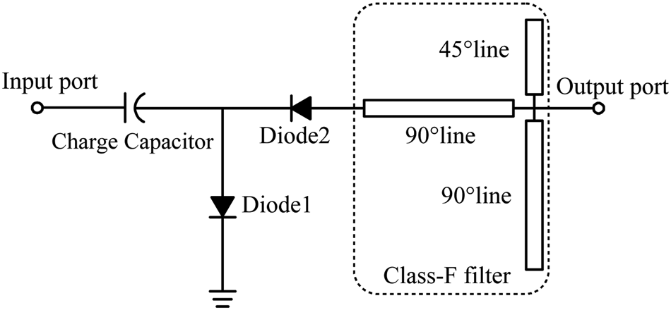
For this system, we proposed a class-F charge pump rectifier that operates in the GHz band [Reference Wang, Mitani and Shinohara5]. The class-F charge pump rectifiers are shown in Fig. 1. In this paper, we theoretically compare the conversion efficiency of a charge pump and single shunt rectifier [Reference Hatano, Shinohara, Mitani, Seki and Kawashima6–Reference Liu, Tan, Zhang and He10], and experimentally verify the results. And considered the application case of the rectenna array, we must understand the load changes when they connect in parallel and series. We elucidate the optimum load changes for the class-F charge pump rectenna array connected in parallel and in series experimentally. The experimental result shows that DC load changes in charge pump rectifiers are the same as single shunt rectifiers. Furthermore, this result also applies to load changes in multi-stage Dickson charge pump rectifiers.
Class-F charge pump rectifier.

2. Conversion efficiency of a rectifier
When a rectifier circuit is performing a rectification operation, the overall loss in the circuit is generated by the circuit elements and transmission lines. The conversion efficiency can be expressed as the difference between theoretical efficiency and transmission line loss, element losses, and the reflection component. This paper mainly discusses single shunt and charge pump rectifiers, their theoretical efficiency is 100%, so the conversion efficiency η can be expressed as equation (1).
 $$\eta = 100\% -L_{TrL}-L_E-{\rm Ref}$$
Here, L TrL is the loss of the transmission lines, L E is the loss of the elements in the circuit, and Ref is the reflection component of the rectifier. When this circuit is in the matching condition, the reflected component is almost 0%. Furthermore, L TrL is very small, and we do not consider the loss of the transmission line in this paper. In a rectifier, we can consider that the conversion efficiency depends on diode loss. The loss of the diode can be expressed by its voltage and current shown as equation (2), where L D is the loss of the diodes. Over a period T, the loss generated by the diodes can be expressed as follows. V is the applied voltage of the diode and I is the current of the diode. In this paper, we use percentages to assess diode losses. Here, the diode we discuss is a non-ideal, and the diode used in the experiment is HSMS2860, please refer to the instruction manual for related parameters.
 $$L_D = \displaystyle{1 \over T}\mathop \int \limits_T^0 VId\theta $$
2.1 The diode voltage and current in a single shunt rectifier
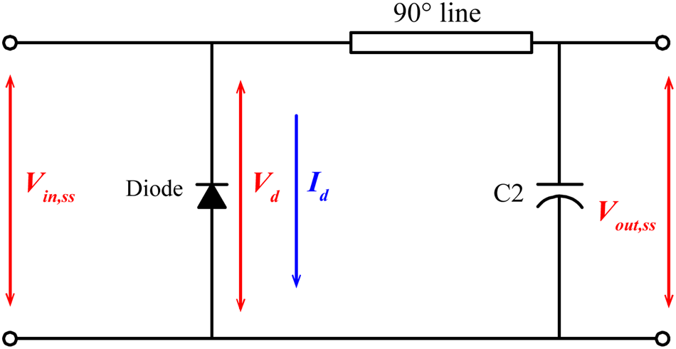
In this section, we discuss the applied voltage and current component in the diode in a single shunt rectifier. We know that the operating state of a diode is mainly affected by its applied voltage. Figure 2 shows the input voltage, output voltage, and applied voltage of the diode in a single shunt rectifier. Voltage V in,ss and V out,ss represent the input and output voltages, respectively. In addition, V d represents the diode voltage. As Fig. 2 shows, V d is equal to V in,ss and V out,ss. In this case, we can assume that the diode current component is I d. The loss in the diode in a single shunt circuit can hence be calculated using equation (2).
Single shunt rectifier circuit.

2.2 The diode voltage and current in a charge pump rectifier
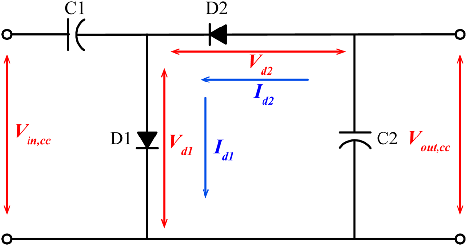
We also analyse the diode voltages and current components in a charge pump rectifier [Reference Honnell11–Reference Borle and Salmon14]. Figure 3 shows the input voltage, output voltage, and applied voltage for the diodes. During the negative half cycle of the sinusoidal input waveform, diode D1 is forward biased and conducts charging up the pump capacitor, C1 to the peak value of the input voltage, (Vp). Because there is no return path for capacitor C1 to discharge into, it remains fully charged acting as a storage device in series with the voltage supply. At the same time, diode D2 conducts via D1 charging up capacitor, C2. During the positive half cycle, diode D1 is reverse biased blocking the discharging of C1 while diode D2 is forward biased charging up capacitor C2. But because there is a voltage across capacitor C1 already equal to the peak input voltage, capacitor C2 charges to twice the peak voltage value of the input signal [Reference Redl and Balogh15]. Hence, capacitor C2 functions as a smoothening capacitor in this circuit. The applied voltages of the diodes are theoretically the same. Voltages V in,cc and V out,cc express the input and output voltages, respectively, of a single-stage charge pump circuit. In addition, V d1 and V d2 are diode voltages in this charge pump circuit. The value of the output voltage, V out,cc is double that of the input voltage, V in,cc. In addition, V d1 and V d2 have the same values. Therefore, V d1 and V d2 equal to V in,cc, and are half of V out,cc. In this case, we can assume that the diode current components are I d1 and I d2.
Charge pump rectifier circuit.

2.3 Diode losses in single shunt and charge pump rectifiers
When the diode applied voltage is near to breakdown voltage, each diode works at its optimum state. In the same input power, if the output voltage increased, the current will reduce. Furthermore, V in,ss is the same as V in,cc, so V d is equal to V d1 and V d2. Under the same input power, we can infer that the current in the diodes, I d1 and I d2 will be half of the current I d. According to equation (2), we can consider the total diode loss is the same in a charge pump and single shunt circuit. It can be concluded that charge pump circuits have almost the same conversion efficiency as single shunt circuits.
2.4 Rectifier experiment result
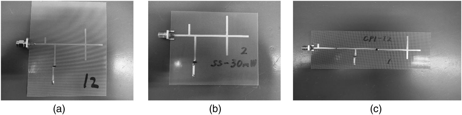
According to the above analysis, when the applied voltage in the diode is the same, the rectifier will have the same conversion efficiency, and the diode applied voltage depends on the input power and DC load. We can control the rectifier efficiency for different input powers by adjusting the DC load, and keep the diode in an optimal working state. To verify this theory, we designed two types of single shunt rectifiers: single shunt rectifier 1 and single shunt rectifier 2. The rectifier 1 operates at an optimum input power of 10 mW and an optimum load of 1000 Ω, the rectifier 2 operates at an optimum input power of 30 mW and an optimum load of 400 Ω. Figures 4(a) and 4(b) show the rectifier 1 and rectifier 2.
Pictures of (a) single shunt rectifier 1, (b) single shunt rectifier 2, and (c) charge pump rectifier.

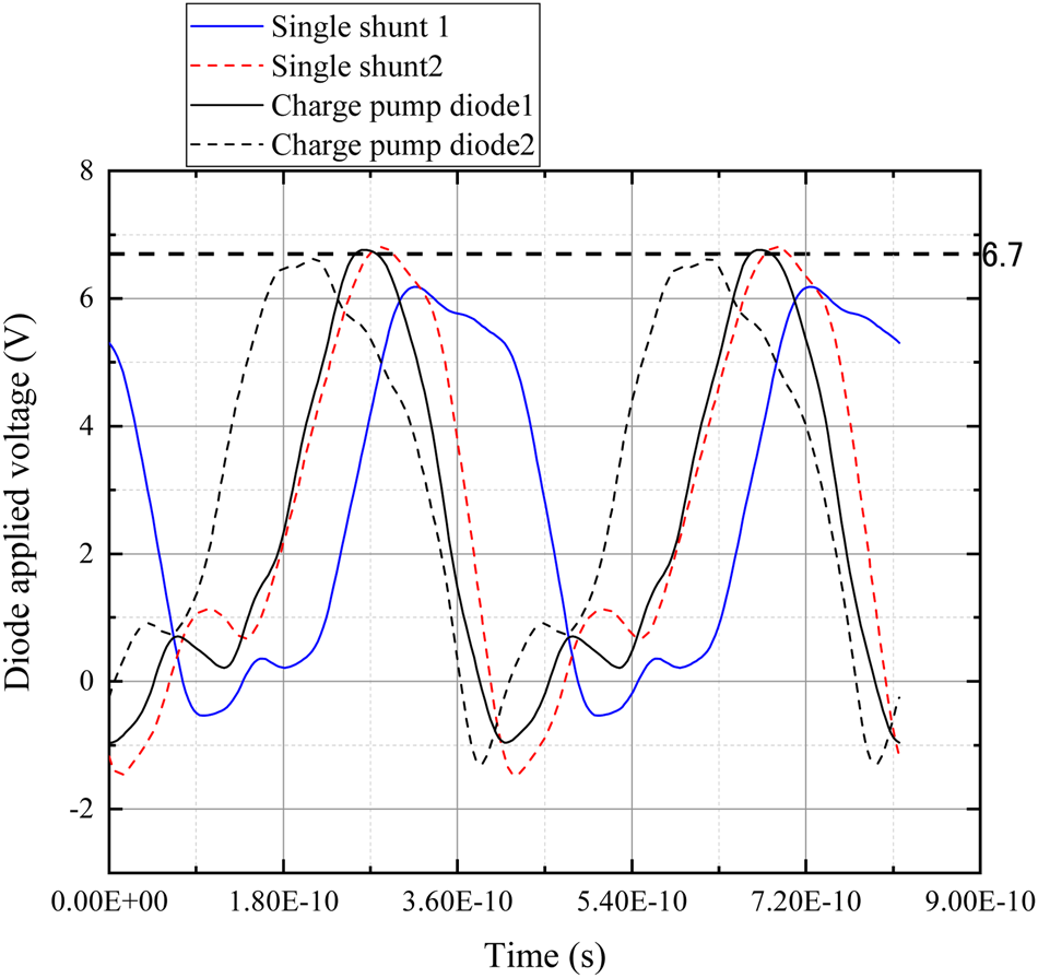
In addition, we designed class-f charge pump rectifiers with an optimum input power of 30 mW and an optimum load of 1400 Ω. Figure 4(c) shows the charge pump rectifiers. We designed the rectifiers have the same diode applied voltage near to their breakdown voltage. Figure 5 shows the diode applied voltage simulation result, and the simulator we used is Advanced Design System. And the HSMS2860 diode breakdown voltage is 7 V.
Applied voltage of the diodes in each rectifier.

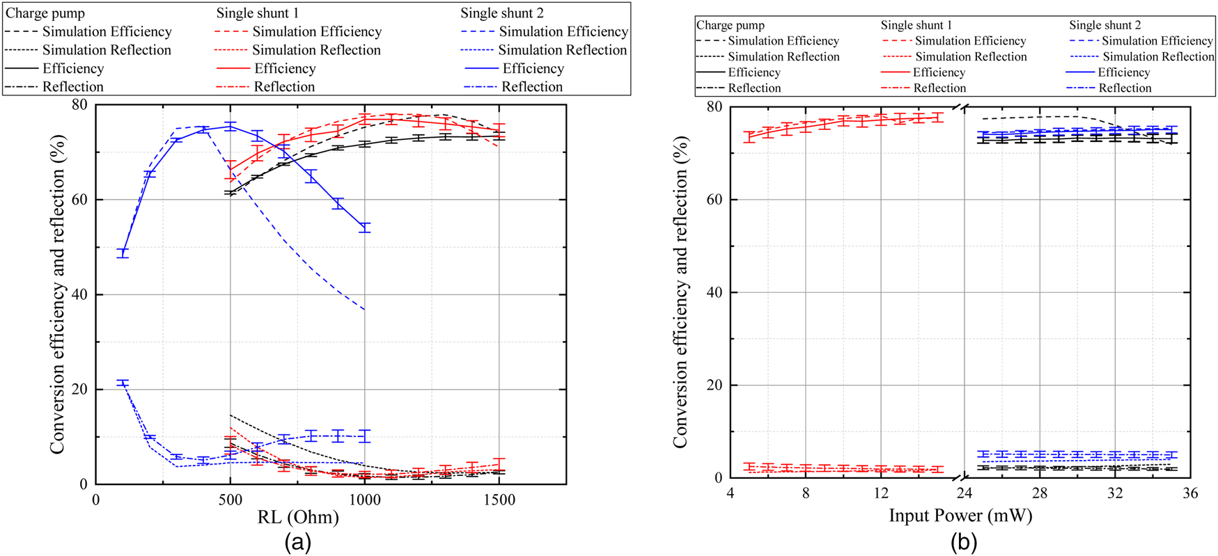
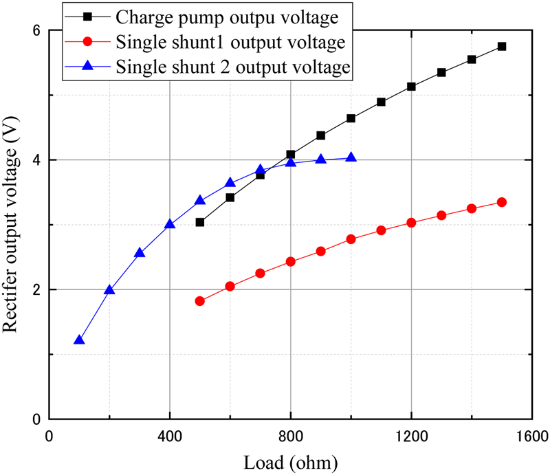
The following experimental data represent the average conversion efficiency and reflection of the rectifiers while the error bars show the standard deviation and the solid line represents the average values. Figure 6 shows the conversion efficiency and reflection of the single shunt rectifier 1, rectifier 2 and charge pump rectifier when the load and input power is sweeping. More than ten of each type rectifier were made, the solid line represents the experimental mean value, error bar represents the experiment data deviation. However, in Fig. 6 the rectifier 2 measurement result, the falling of conversion efficiency is not consistent with the simulation data. The reason can be attributed to the fact that diode breakdown voltage is higher than the datasheet given breakdown voltage, whereby the load exceeds the optimum load in the simulation. However, the efficiency is consistent with the simulation data near the optimum load. From this experimental result, we can observe the efficiency is about 79% whether rectifier 1 or rectifier 2. Although the input power is different, their conversion efficiency percentage is the same at the same diode voltage. From the black lines, the simulation charge pump rectifier efficiency is about 78% and the experimental efficiency is 73%. The difference of simulation and experiment result is caused that the complicated transmission line generated more loss than rectifier 1 and rectifier 2 in the charge pump rectifiers. Figure 7 shows the output voltage of each rectifier. As shown in Fig. 7, rectifiers 1 and 2 output about 2.7 V at each optimum load, the output voltage of the charge pump rectifier is about 5.5 V. And the single shunt output voltage is half of the charge pump output voltage, this result proves that both circuits are in the correct working state.
Reflection and conversion efficiency of the rectifiers, with (a) sweeping load and (b) sweeping input power.

The output voltage of single shunt 1, single shunt 2, and charge pump rectifier.

3. Rectenna array experiment and result
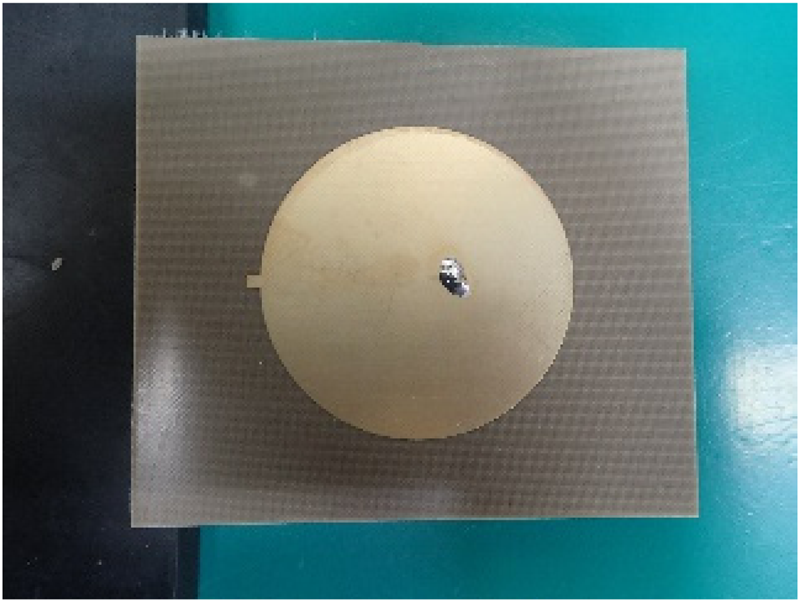
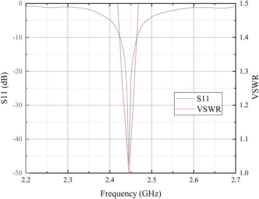
In this chapter, we consider the application scenarios of class-f charge pump rectenna arrays. In many previous research, the load changes be discussed when single shunt rectifiers were connected in parallel or series. The result shows that the optimum load of a single shunt rectenna array with N elements connected in parallel will change to 1/N, and to N times when they are connected in series [Reference Shinohara and Matsumoto16–Reference Shinohara and Matsumoto19]. The essence is to keep the output voltage of every rectifier consistent. The output voltage has a linear relationship with the diode applied voltage of single shunt rectifiers, and the optimum load change is to adjust the applied voltage of the diodes for each rectenna connected in parallel or series. Thus, according to Conversion efficiency of a rectifier and the points noted above, we note that the optimum load of a charge pump rectenna array follows the same law as a single shunt rectenna array. Figure 8 shows the antenna used in this experiment. Figure 9 shows the S11 and VSWR of the antenna. In the following experiment, we adjusted the transmission distance and the antenna position so that each received power of antenna elements is about 36 mW. So the antenna pattern figure can be omitted here, and Figure 10 is shows the experiment photos.
The photo of the 2.45 GHz antenna.

The S11 and VSWR of the 2.45 GHz antenna.

The rectenna array photos.

The class-f charge pump rectifiers shown in Fig. 4(c) were used in this experiment. The experiment was conducted to measure the output voltage and rectenna efficiency in a 2 by 2 charge pump rectenna array connected in parallel and in series. According to the theory stated above, the effective optimum load will be 350 and 5600 Ω when the rectenna array is connected in parallel and in series, respectively. Figures 11 and 12 show the rectenna efficiency and output voltage for the charge pump rectenna array connected in parallel and series, respectively. From the figures, the rectenna array exhibits the same efficiency as the rectifier near the theoretical optimum load. This is exactly the same as the theoretical efficiency of the single shunt rectenna array, and the load changes are exactly the same as the single shunt rectenna arrays.
The result of the class-f charge pump rectifier rectenna array connected in parallel.

The result of the class-f charge pump rectifier rectenna array connected in series.

4. Conclusion
In this paper, we explored the relationship between the conversion efficiency and applied voltage in a diode. We verified the theory with two types of single shunt rectifiers, and obtained similar conversion efficiencies. And we compared the new type of charge pump rectifier that we designed with the two types of single shunt rectifiers, and found that the experimental results show good agreement with the theory. The results indicate that they exhibit almost the same conversion efficiency. Based on the above observations, we calculated the optimum load of the charge pump rectenna array connected in parallel and in series. We experimentally verified the change in the optimum load of the charge pump rectenna array and found that the optimum load of a class-f charge pump rectenna array with N elements connected in parallel will change to 1/N, and to N times when they are connected in series. It is consistent with the results obtained for the single shunt rectenna array.
In future applications, the load changes of the charge pump rectenna array can use the same estimation method as single shunt rectenna array. We will design a multi-stage Dickson charge [Reference Kashiwase20] pump and Cockcroft–Walton circuit [21] based on this class-f charge pump rectifier in the future. The above conclusions will also help us understand the load changes of multi-stage charge pump circuits.
 Ce Wang (S’–) received the M.S. degree from the electrical engineering at Kyoto University, Kyoto, Japan in 2016. He is currently pursuing Ph.D. degree in electrical engineering at Kyoto University, Kyoto, Japan. His current research interests include low-power rectenna and wireless power transmission system design.
 Bo Yang was born in Zhenjiang Province, China, in 1986. He received the B.S. degrees in Electronic Information Engineering from China University of Petroleum (East China) in 2008 and received M.E. degree in electronic engineering from Kyoto University in 2018. From 2008 to 2015, he has been working as an RF engineer with the DAIHEN group, Qingdao, China. Currently, he is working toward Ph.D. degree in electrical engineering at Kyoto University, Kyoto, Japan.
 Seishiro Kojima received B.E. degree in electrical and electronic engineering and M.E. degree in electric engineering from the University of Kyoto in 2015 and 2017, respectively. Currently, he is pursuing Ph.D. degree in electric engineering. He is a student member of the IEEE and the Institute of Electronics, Information and Communication Engineers (IEICE).
 Naoki Shinohara received the B.E. degree in electronic engineering, the M.E. and Ph.D (Eng.) degrees in electrical engineering from Kyoto University, Japan, in 1991, 1993 and 1996, respectively. He was a research associate at the Radio Atmospheric Science Center, Kyoto University from 1996. He was a research associate of the Radio Science Center for Space and Atmosphere, Kyoto University by recognizing the Radio Atmospheric Science Center from 2000, and there he was an associate professor since 2001. He was an associate professor in Research Institute for Sustainable Humanosphere, Kyoto University by recognizing the Radio Science Center for Space and Atmosphere since 2004. From 2010, he has been a professor at Research Institute for Sustainable Humanosphere, Kyoto University. He has been engaged in research on Solar Power Station/Satellite and Microwave Power Transmission system. He is IEEE Distinguish Microwave lecturer, IEEE MTT-S Technical Committee 26 (Wireless Power Transfer and Conversion) vice chair, IEEE MTT-S Kansai Chapter TPC member, IEEE Wireless Power Transfer Conference advisory committee member, international journal of Wireless Power Transfer (Cambridge Press) executive editor, Radio Science for URSI Japanese committee C member, past technical committee chair on IEICE Wireless Power Transfer, Japan Society of Electromagnetic Wave Energy Applications vice chair, Wireless Power Transfer Consortium for Practical Applications (WiPoT) chair, and Wireless Power Management Consortium (WPMc) chair.