I. INTRODUCTION
Emerging system applications, including future high-speed communications, high-resolution radar/imaging systems and directed energy are driving the need for W-band power amplifiers (PAs) [Reference Samoska1–Reference Brown5]. In general, two PA parameters are the subject and target of intensive research: high output power and high efficiency [Reference Daneshgar3–Reference Brown5]. Recently, reconfigurability has been added as an important topic for PA operation and design. The higher the transmitted power the larger is the transmission range, while high efficiency extends battery lifetime, saves energy, and reduces system complexity and cost. This work focuses on improving the PA efficiency. Common PAs in the millimeter wave range apply the class-A, -AB [Reference Samoska1, Reference Daneshgar3–Reference Brown5], or even class-E design approach [Reference Song6]. As these types of PAs are narrowband and the transistors require a proper input and output matching they are limited in terms of flexibility, reconfigurability, and compactness. To overcome these limits, the digital PA approach is a suitable candidate, well proven in the lower GHz-range [Reference Wentzel7], but never employed in the sub-THz region so far. This paper presents for the first time a W-band PA following the digital approach [Reference Wentzel, Hossain, Stoppel, Weimann, Krozer and Heinrich8].
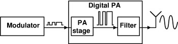
Figure 1 illustrates the concept: A digital data stream feeds the digital power amplifier (DPA). Then, the PA stage amplifies the bit stream in amplitude and the analog filter at the output reconstructs the wanted signal. Ideally, the transistor in the PA stage operates only in on- and off-state leading to a very high efficiency. The challenge is to realize the output filter and high-power levels. The paper is organized as follows: Section II introduces the MMIC technology used. Section III briefly describes the digital amplifier designs, while Section IV presents the measurement results, including small- and large-signal characterization. Finally, Section V concludes the paper.
Principle of DPA, including PA stage and analog output filter.

II. MMIC TECHNOLOGY
The MMIC process utilizes InP DHBT devices transferred onto an AlN carrier wafer by use of an adhesive wafer-bonding process, which reduces the extrinsic base-collector capacitance C bcx and facilitates heat extraction from the active device region [Reference Weimann9].
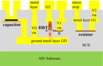
The cross-section of the technology layers is shown schematically in Fig. 2, including thin-film SiN X capacitors with 0.3 fF/µm2, NiCr resistors with 25 Ω/square and metal resistors with 0.5 Ω/square, along with gold-filled via connections between the three layers of routable interconnect metal (Gd, G1, G2), with thickness ranging from 1.2 to 4.5 µm. BCB is used as an interlayer low permittivity dielectric. The p-base (B) has a thickness of 30 nm, the emitter (E) with the cap has a height of 160 nm, the collector (C) with setback, delta doping, sub-collector, and grade are 155 nm thick. Microstrip waveguide connections are formed between G2 and the RF ground plane Gd, with 5 µm BCB between the conductor layers. An i-line stepper has been used to define all lithography steps. The double-finger InP DHBTs with 2 × 0.8 × 6 µm3 emitter area exhibit extrinsic f T /f max of 350/300 GHz at 40 mA collector current. A DC current gain β of 45 and a breakdown voltage V BD, CEO beyond 4 V is achieved. Heat sinking to the AlN carrier substrate is facilitated through the inclusion of deep gold-filled vias (VX) reaching the top of the AlN substrate.
Cross-section of transferred-substrate InP DHBT MMIC technology used for realized digital PA MMIC.

As the targeted signal frequency f S of 100 GHz is nearly only one third of the current gain transition frequency (350 GHz) an operation of the amplifiers with clean rectangular signals which require several higher harmonics of f S (up to at least 1 THz) is not possible. However, the following section describes a first digitally designed PA approach in the 100 GHz range. But due to technology limits (f T /f max) the proposed amplifiers will not operate as purely digitally switched ones. The fact that the final setup is planned to utilize a digital modulator and a dedicated preamplifier for proper (digital) driving of the PA (cp. Fig. 1), the presented amplifier will be termed as “digital” in the following although these types of sinusoidal-driven PAs are often called “switch-mode”.
III. DPA DESIGN
The DPAs were realized using our in-house 0.8 µm InP HBT transferred substrate process as described above. First, the single-band design is explained.
A) Single-band DPA
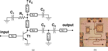
The schematic of the circuit is shown in Figs 3(a), while 3(b) exhibits a photograph of the fabricated DPA MMIC.
(a) Schematic representation of realized single-band digital PA MMIC, including collector bias feed, BPF, and matching to 50 Ω for 95 GHz; (b) Photograph of fabricated InP DHBT S-DPA MMIC for 95 GHz; chip area (w/pads): 0.51 × 0.53 mm2.

The S-DPA utilizes a two-emitter-finger InP DHBT with an area of 2 × 0.8 × 6 µm3 as an active device (T 1 in Fig. 3(a)). The transmission lines TL1 and TL7 represent the 50 Ω input and output line, respectively. TL2, TL3, and TL4 together with the blocking capacitors C1/2 and the resistor R 1 form the collector bias network. The base of the HBT is biased with an external bias-T (not shown in Fig. 3(a)) connected at the input of the PA. At the output of the transistor, TL5 (120 µm) together with capacitor C3 (120 fF) builds the band-pass filter (BPF). TL6 (330 µm) and C4 (100 fF) match the filter to 50 Ω output for a center frequency of 95 GHz.
In contrast to the well-known analog PA concepts the transistor in the digital approach does not need any reactive matching at the input and output, respectively. This saves chip area and cost. Ideally, the amplifier can operate in a very broadband frequency range with switchable output filter bank. This is a major advantage of this type of PA. Figure 3(b) shows the fabricated PA MMIC exhibiting a compact chip area of only 0.51 × 0.53 mm2 including the pads.
The HBT must be biased at the input with a certain base current I B . Thus, for digital operation a large I B -swing is required to switch the devices truly on and off. In this work, this is realized by biasing the base with a voltage V B and providing a voltage swing with a common RF signal source.
To operate the digitally designed PAs in a truly digital mode the amplifier must be driven at the input with a rectangular signal (cp. Fig. 1), which has the carrier frequency encoded. In order to apply such a signal in the 100 GHz-range a source up to at least 1 THz or clipping the signal using Schottky diodes would be required. As both sources were not available and due to the frequency limits of the used technology (see Section II) we applied an overdriven sinusoidal input signal with a maximum amplitude of 1.7 Vpp (9 dBm) to the HBT's base to emulate the digital operation. In simulation, it turned out that the overdriven harmonic signal gives a good estimation of the digital operation behavior. But one has to state that in digital operation the varying input power is modulated by changing the duty-cycle of the input signal, for example, while input amplitude stays constant. This is not the case when using an overdriven sinusoidal input signal where the amplitude changes. Hence, only the full-scale case, i.e. 50% duty-cycle in a pulse-width-modulated signal for instance, can be emulated by the proposed strong sinusoidal overdrive.
However, the PA is optimized for broadband digital input signals. Therefore it does not include any reactive matching. Hence, we have to apply in this measurement a single sine input signal at 95 GHz with a rather high-input voltage swing of 2.5 Vpp (12 dBm) to generate the required swing (1.7 Vpp) at the base. Consequently, in terms of power-added efficiency (PAE) calculation, the available signal source input power (max. 12 dBm) is taken into account. It is important to note that the results would be improved with a rectangular signal source. The PAE is calculated as the ratio between output power P out and the sum of overall DC power P DC as well as the available signal source input power P in .
B) Dual-band digital power amplifier (D-DPA)
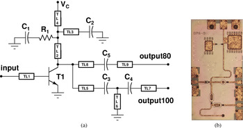
In order to check the multi-band capabilities of the DPA approach, a dual-band PA has been designed and realized. Again, the circuit was fabricated using the FBH 0.8 µm InP DHBT transferred substrate process (cp. Section II) and no special reactive matching as usual in common PA designs has been applied. Figures 4(a) (left) and 4(b) (right) show the schematic and photograph of the realized D-DPA MMIC, respectively.
(a) Schematic representation of realized D-DPA MMIC including collector bias feed, dual-band filter and matching to 50 Ω; (b) Photograph of fabricated D-DPA, chip area (w/pads): 0.46 × 0.85 mm2.

The D-DPA applies the same two-finger DHBT as active device as the single-band design (2 × 0.8 × 6 µm3). The output network of the amplifier combines two series BPFs in parallel, but with separate output port: one filter branch resonating at 80 GHz (denoted as f 1 in the following) and a second optimized for 100 GHz (f 2). The f 1-branch (output port “output80” in Fig. 4(a)) utilizes TL8/9 and C5 (60 fF) as filter elements, while the f 2-branch with output port “output100” (cp. Fig. 4(a)) represents the single-band BPF used in the S-DPA design (cp. Fig. 3(a)). In case of an 80 GHz input signal one has to probe on “output80” – pad to measure the appropriate output signal, while “output100” is open. In case of 100 GHz input, the “output100” – pad must be used and “output80” is open. Moreover, the input line and bias network are the same as used in the S-DPA. Owing to the extension of the output network the MMIC requires more space, but still exhibiting a compact chip area of 0.39 mm2. In further realizations, frequency bands in W- and G-bands will be covered at the same time, respectively.
IV. MEASUREMENTS
A) Small-signal characterization: BPF
In order to determine the optimum signal frequencies f S for the operation of the two DPAs, the S-parameters of the integrated BPFs are checked. All S-parameters on wafer (TSML calibration method) were measured using Agilent's PNA system from 50 MHz–110 and from 140 to 220 GHz with an RF input power (P in ) of −23 dBm.
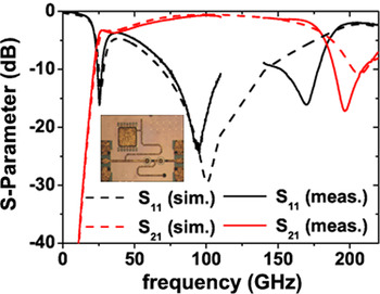
First, the S-parameters of the single-band BPF (TL5/6, C3/4 in Fig. 3(a)) are presented. Note that the collector bias feed transmission line TL2 (cp. Fig. 3(a)) is taken into account as it has a certain influence on the filter characteristic. Figure 5 presents the simulated and measured input return loss (RL) (S 11) and insertion loss (IL) (S 21), respectively. A chip photograph of the output filter MMIC is shown as an insert in the diagram.
Simulated and measured S-parameters (0.05–110, 140–220 GHz) of single-band BPF, including matching and collector bias feed line, P in = −23 dBm; detail: realized BPF MMIC including matching and collector bias feed line; chip area (w/o pads): 0.3 × 0.3 mm2.

From Fig. 5 one clearly recognizes a small frequency shift from 100 GHz down to 95 GHz between simulation and measurement in terms of optimum input RL S 11. Measured S 11 at 95 GHz is −24 dB. The IL S 21 is shifted as well; it exhibits a minimum value of 0.6 dB at 95 GHz. The shift in frequency is due to the tolerances of the discrete on-chip capacitors used in the design of the BPF, though the ±5%-tolerance of capacitor value lies within the specifications of the InP DHBT process. Some more discrepancies between simulation and measurement can be observed in G-band. However, the BPF significantly suppresses the second harmonic (190 GHz) by 11 dB. This is important for an efficient DPA behavior. But, again, the PA itself (w/o filter) is designed to be broadband.
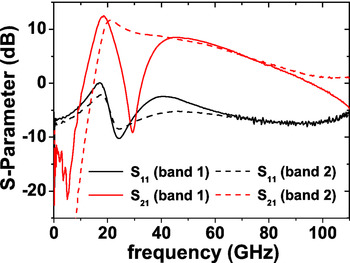
Figure 6 presents the S-parameters (S 11 and S 21) of the dual-band BPF designed for 80 GHz (f 1) and 100 GHz (f 2), respectively. To have a clear view of the data, the diagram displays only measured S-parameters of the two filter branches according to Fig. 4(a): (i) input to output80, which will be denoted as frequency “band 1” in the following; (ii) input to output100, denoted as frequency “band 2”. Again, the collector bias feed lines as well as blocking capacitors (cp. Fig. 4(a), TL8/9, C5) are taken into account.
Measured S-parameters (0.05–110, 140–220 GHz) of dual-band BPF including matching and collector bias feed line, P in = 23 dBm; detail: realized dual-band pass filter MMIC; chip area (w/o pads): 0.7 × 0.3 mm2.

From Fig. 6 one clearly observes the two different center frequencies f 1 and f 2 of the dual-band filter. IL and RL show the best results at 68 GHz (f 1) and 76 GHz (f 2), respectively. The filter exhibits an IL (S 21) of minimum 0.7 dB in both frequency bands, while an input RL of more than 21 dB is achieved. Accordingly, the D-DPA will be operated in these frequency bands with regard to power measurements. Moreover, Fig. 6 includes the G-band information. Thus, the suppression of the second- and third-harmonic frequency of both bands can be approximately extracted. For “band 1” (68 GHz) the second and third harmonic is suppressed by 4.4 dB (−5 dB) and 14.2 dB (−14.8 dB), respectively. The second harmonic of “band 2” is suppressed by 3 dB (−3.6 dB). Here, the third harmonic (228 GHz) lies out of the measurement range (0.05–110, 140–220 GHz), but one can estimate it to be at least 18 dB by taking the value at 220 GHz. Summarizing these results one can conclude that the rejection of the second harmonics must be improved, which will also improve further the overall efficiency of the PA in two band operation.
Mainly, one has to state that there is a clear shift in frequency of operation for both bands as the filter parts were designed to resonate at 80 and 100 GHz. This may arise due to inaccurate simulations and thus design. For this first dual-band approach no EM simulation was performed in advance. In a second design for one of the next process runs these EM simulations have been conducted and they show that the frequency is shifted due to improper modelling of the SiN X caps and due to an inaccurate microstrip line definition. This will be improved in future designs. However, although the frequency of operation is shifted that much a demonstration of the multi-band operation was possible and has been performed in the bands derived above.
B) Small-signal characterization: digital PAs
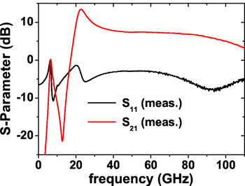
Figure 7 shows the measured S-parameters of the whole single-band DPA from 0.05–110 GHz. Here, the HBT (T 1 in Fig. 3(a)) is biased with a base current I B of 0.7 mA and a collector voltage V C of 2.7 V. The high admissible collector emitter voltage shows the advantage of DHBT technology. From Fig. 7 one can identify a very broadband behavior of the DPA exhibiting a gain of 7 ± 3 dB from 25 GHz up to beyond 110 GHz. At the signal frequency of 95 GHz the small-signal gain is 5.6 dB. Below 20 GHz one clearly recognizes the influence of the integrated BPF showing a significant suppression of the frequency components down to DC (cp. Fig. 5). Moreover, a fair input matching of −8 dB at 95 GHz is achieved although no specific matching was applied, which demands a higher source input power to generate the needed V/I-swing at the HBT's base.
Measured S-parameters (0.05–110 GHz) of realized S-DPA; P in = −23 dBm; bias: I B = 0.7 mA, V C = 2.7 V.

To check the influence of the dual-band output network on the small-signal characteristics the D-DPA is also measured with an input power of −23 dBm from 0.05–110 GHz. Figure 8 exhibits the measured S-parameters (S 11 and S 21) for band 1 (from “input” branch to “output80” in Fig. 4(a)) and band 2 (“input” to “output 100” branch in Fig. 4(a)), respectively. Both characteristics are again measured in W-band (0.05–110 GHz) with a small RF input power of −23 dBm, an I B of 0.7 mA and a collector voltage V C of 2.7 V, i.e. the same conditions applied for the single-band case.

The realized dual-band module achieves a small signal gain of 5.7 dB at 68 GHz for the first frequency band (“band 1” in Fig. 8) and an even smaller value of 4.3 dB at 76 GHz in the 2nd band (“band 2”). Maximum gain is 12.5 dB at 20 GHz. As already recognized in the single-band measurement the output filters of the PA also have a clear influence on the gain characteristics leading to significant suppressions of the frequency components below 20 GHz down to DC. This is clarified especially when comparing both S 21-characteristics of the filters (cp. Fig. 6) with the ones in Fig. 8. Also, due to the output filters the gain at frequencies above the two carriers (f 1 = 68, f 2 = 76 GHz) is strongly decreased. Again, a sufficient input matching of about –7 dB is reached in both frequency bands.
C) Large-signal characterization
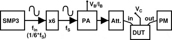
First, Fig. 9 shows the measurement setup used to characterize the DPAs. For the single-band measurement at 95 GHz, e.g. the signal generator SMP3 from Rohde & Schwarz generates the sinusoidal input signal at 15.833 GHz. Then, the signal frequency is multiplied by 6 to 95 GHz with an active frequency multiplier (AFM6 75-110) from Radiometer Physics GmbH. After this the signal is amplified by means of a W-band packaged MMIC PA (WPA-10-882015) from Wasa Millimeter Wave AB.
Measurement setup for large-signal characterization of proposed S- and D-DPAs.

Moreover, the W-band preamp includes a bias-T, which is used to bias the base of the realized DPA. Finally, the input signal is attenuated with a waveguide tunable attenuator (WTA-110), again from Radiometer Physics GmbH, to fully control the input voltage swing. The DUT is connected at input and output with RF W-band on-wafer probes. The collector biasing is connected with the PA via DC needle. At the output the HP 437B power meter (PM) using W8486A power sensor measures the output power.
As already explained in Section III-A the digitally designed amplifiers can only be driven with (overdriven) sinusoidal signals to emulate full-scale (50% duty-cycle) PWM operation due to the limits of the measurement equipment available to date. However, although the proposed PAs are not driven with a digital modulator and thus in a truly digital mode the test procedure is a suitable way to check the potential of the concept, but only in terms of full-scale input. In the future, one could think of designing multipliers without suppressing harmonics in order to generate rectangular input signals and to overcome the frequency limit problem. But this needs to be realized on an InP HBT process with a smaller emitter area to reach higher f T /f max .
To check the optimum performance of the DPAs (including BPF) in terms of input power, a P in -sweep from −4 to 12 dBm of available source input power (P in_available ) is initially performed. The maximum P in_available of 12 dBm translates, according to simulations, into a real maximum input power of 9 dBm at the base of the HBTs (T 1 in Figs 3(a) and 4(a)). This is due to no special reactive input matching applied in the design. The 9 dBm of P in correspond to a voltage swing of 1.7 Vpp. According to simulation this translates into a ± 40 mA current swing with a mean DC value of 1 mA (I B ), which represents the limit for the transistor. As already mentioned in Section III, PAE is calculated with the signal source power needed to generate the desired swing at the base (max. 12 dBm).
Moreover, both DPAs are characterized for varying collector voltages V C (1 to 2.7 V) at P in_available of 8, 10, and 12 dBm. First, the results of the S-DPA are presented and discussed.
1) SINGLE-BAND DPA
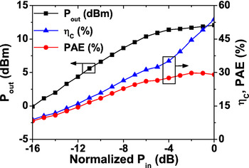
Figure 10 presents the measured results of the S-DPA for an input power sweep (normalized to 12 dBm P in ). Output power P out , collector efficiency η C and power-added efficiency (PAE) are plotted for a constant collector voltage V C of 1.6 V. Collector efficiency is the relation between the dissipated DC power only at the collector (P C ) of the PA and the output power at the load (P out /P C ), while PAE is calculated as P out /(P DC + P in ). If one would use the common PAE definition ((P out –P in )/P DC ) the input power P in is the real maximum input power, i.e. 9 dBm for a P in_available of 12 dBm.
Measured output power (P out ), collector efficiency (η C ) and PAE of the S-DPA versus normalized input power (P in ); bias: V B = 0.85, V C = 1.6 V; P in normalized to 12 dBm available source input power.

In Fig. 10, one observes an increase of P out with growing P in peaking at 12.1 dBm. The behavior is almost linear up to 5 dB below maximum input power. The PAE saturates at 30%. In contrast, the collector efficiency η C increases over the whole P in -range and reaches 54%. With regard to optimum performance, a P in_available between 8 and 12 dBm is the best choice for this circuit. Additionally, one can observe a relatively small drop in PAE between full-scale and backed-off input power of −6 dB from 30% down to 26%, respectively. This is important to note since next-generation 5G high-speed communication networks will demand for high efficiencies over a wide power back-off range, typically down to −12 dB.
But one has to state that this is different from a digital operation where the modulated input power is varied for example with a varying duty-cycle of a rectangular signal with constant amplitude in a fixed-time period. Compared with this the measurement in Fig. 10 varies the input amplitude of the sinusoidal input signal up to a certain overdrive. Thus, the P out and PAE in a digital mode may differ from the values achieved using saturated CW excitation.
The performance can be further improved with additional driver stages operating near transistor cut-off at lower collector voltages as indicated below. This will help to switch the power stage and improve the overall gain of the DPA.
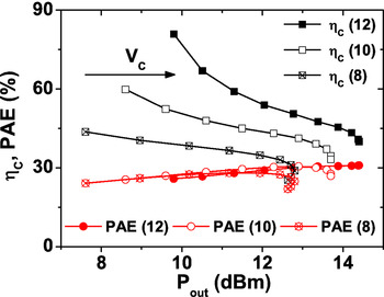
Now, the collector voltage V C is swept from 1 to 2.7 V for 8, 10, and 12 dBm available source input power. Figure 11 displays the measured characteristics of η C and PAE as a function of P out . For V B of 0.85 V (I B -limit: 1 mA) and V C of 2.7 V the digital PA achieves its maximum PAE of 31% at a saturated P out of 14.4 dBm. Although this is not the highest PAE reported in W-band to date [Reference Song6], the result is sufficient taking into account that this is the first W-band DPA realization so far. Even more if one would calculate PAE with the real input power at the base. Furthermore, from Fig. 11 one clearly observes a drop in η C with rising collect1or voltage V C and therefore P out . For example, at 12 dBm input power (curve η C (12) in Fig. 11) the collector efficiency decreases from 81% (V C = 1 V) to 40% (V C = 2.7 V). The peak value proves the great potential of the proposed digital PA. But, basically, the self-heating of the devices with increasing V C and thus P out influences significantly the performance. This needs to be solved in future work.
Measured collector efficiency (η C ) and PAE of the S-DPA for varying collector voltages V C (1 to 2.7 V) and 8, 10, and 12 dBm input power versus output power (P out ); V B = 0.85 V.

Moreover, for the same bias conditions the S-DPA exhibits a measured small-signal gain of 5.6 dB at 95 GHz with −8.1 dB of input RL. Summarizing the results one has to state that they are very competitive in terms of P out and small-signal gain [Reference Daneshgar3] (downscaled to the same emitter finger-width and transistor size) as well as PAE [Reference Daneshgar3–Reference Song6]. This is true in particular when taking into account that the proposed DPA utilizes a comparatively large emitter finger-length (0.8 µm), but is much more compact compared with [Reference Daneshgar3–Reference Song6] and, in contrast to [Reference Daneshgar3–Reference Brown5], does not apply any combining. Power combined stages will be realized in future designs.
2) DUAL-BAND DPA
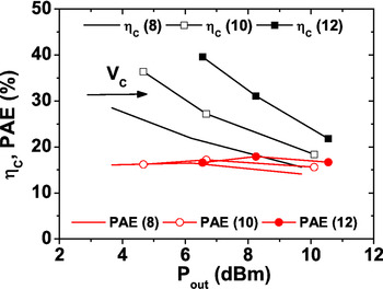
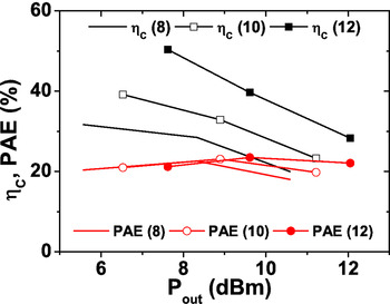
Finally, the D-DPA is characterized in large-signal measurements. Figures 12 and 13 show the measured collector efficiency (η C ) and PAE versus the output power (P out ) for different collector voltages V C (1, 1.5, and 2.7 V) and RF input powers (8, 10, and 12 dBm), available at the source. While Fig. 12 depicts the data for an input signal frequency of 68 GHz (f 1), i.e. “band 1”, which is probed at output pad “output80” in Figs 4(a), Fig. 13 shows the characteristics for 76 GHz input signal frequency in “band 2” (f 2), which is probed at the “output100” (Fig. 4(a)). An input power sweep at a fixed V C like displayed in Fig. 10 was not performed for the D-DPA.
Measured collector efficiency (η C ) and PAE of the D-DPA at frequency “band 1” (input to “output80” in Fig. 4(a)) for varying collector voltages V C (1, 1.5, and 2.7 V) and 8, 10, and 12 dBm available source input power versus output power (P out ); V B = 0.85 V; f S = 68 GHz.

Measured collector efficiency (η C ) and PAE of the D-DPA at frequency “band 2” (input to “output100” in Fig. 4(a)) for varying collector voltages V C (1, 1.5, and 2.7 V) and 8, 10, and 12 dBm available source input power versus output power (P out ); V B = 0.85 V; f S = 76 GHz.

The D-DPA achieves for 68 GHz input signal frequency (“band 1”) a maximum output power of 11 dBm with a peak PAE of 18%. This is much lower than in the single-band case (cp. Fig. 11). Collector efficiencies are increasing with more RF input power (from 8 to 12 dBm) and show peak values of 40%. The significant lower output powers and thus efficiencies are mainly due to the interaction between the two filter branches (see Fig. 4(a)). Because of that the impedances presented by the output network to the transistor are not optimum. This degrades performance. Moreover, both filters show a shift of the resonant frequency, which is another indicator of insufficient design procedures in advance. This means in future work one must apply EM simulation in order to take into account all effects of the circuit, no matter how simple it may be. However, for a first multi-band approach the results are still very sufficient. Figure 13 presents the measured results for an input signal frequency of 76 GHz.
In the second frequency band of operation slightly better results can be observed. The PAE peaks at 24% for a maximum P out of 12.1 dBm, measured at the “output100” branch of the D-DPA (cp. Fig. 4(a)). Furthermore, the collector efficiencies in this frequency band achieve 50% at the maximum, which shows again the big potential of the digital design approach. Also, as already described below Fig. 12, the results are degraded when comparing them to the S-DPA.
Table 1 summarizes the performance comparison with recent W-band PAs. In order to get a clearer view for the compared values and to set the chip area in relation to the delivered output power the second row of the table shows size of the output stage for each reference. In the last line, the values after the “S:” represent the measured data of the single-band PA, while after the “D:” in Table 1 the data of the dual-band version is given.
Summary of recent W-band PAs.

The table clearly indicates that high-efficiency concepts can deliver high output power and high efficiency at millimeter-wave frequencies with very high-power density. The work on class E PA is bandwidth limited, while the concept of DPA can outperform other PAs when several devices are combined into a larger power cell. The major advantage of the digital PA is the reconfigurability, flexibility (multi-band operation) and thus compactness and low cost.
V. CONCLUSION
Two highly efficient DPA MMICs have been designed and realized in W-band for the first time: a single-band PA (S-DPA) at 95 GHz and a dual-band version (D-DPA) at 68 GHz (band 1) and 76 GHz (band 2), respectively, to prove the flexibility in terms of signal frequency due to the broadband approach. The circuits have been fabricated on FBH in-house 0.8 µm InP DHBT transferred-substrate process. The DPAs do not apply any reactive matching for the transistors at in- and output, which leads to a very compact chip size of 0.27 and 0.39 mm2 only. The integrated BPFs show a minimum IL of 0.6 dB and an input RL of more than 20 dB, respectively. The single-band PA (including BPF) reaches a maximum P out of 14.4 dBm with peak PAE of 31%. Small-signal gain is 5.6 dB. The dual-band amplifier shows a gain of 5.7 dB in band 1 (68 GHz) and 4.3 dB in band 2 (76 GHz). The D-DPA shows peak output power of 12.1 dBm and PAE of 24%, respectively. These values are much lower than in the single-band case, but may be improved when redesigning the structure with EM simulation tools, which were not used for this first dual-band design.
However, summarizing the results one can conclude that together with measured collector efficiencies above 80% the great potential of the DPA for future wireless high-speed communication systems is well proven. Further work on high-frequency DPA will focus on mitigating the self-heating induced drop in efficiency as well as on combining several PA cells to achieve higher P out , gain and efficiency. Furthermore, it is planned to realize a multi-band PA suitable for W- and G-band applications.
ACKNOWLEDGEMENTS
The authors would like to thank FBH's process technology staff for wafer fabrication. Moreover, A. Wentzel likes to thank M. Hrobak for the great help in characterizing the circuits, especially in terms of the dual-band DPA. N. Weimann acknowledges partial funding from the European Union Seventh Framework Programme (FP7/2007-2013) under grant agreement no 333858.
 Andreas Wentzel received the Dipl.-Ing. and Dr.-Ing. degrees in Electrical Engineering from the Technical University of Berlin, Germany, in 2006 and 2011, respectively. Currently, he is the Head of the Digital PA Laboratory in the III–V-Electronics Department of the Ferdinand-Braun-Institut in Berlin. His research activities focus on the design of digital TX architectures, including advanced switch-mode power amplifier concepts realized on GaN and InP as well as on optimized modulation schemes and filter structures suitable for this type of PA.
 Maruf Hossain received his M.Sc. degree in Electronics/Telecommunication from the University of Gavle, Gavle, Sweden in 2008 and Ph.D. degree in Electrical Engineering from Technical University of Berlin, Berlin, Germany in 2016. In 2008, he joined in IHP microelectronics in the Circuit Design Department, Frankfurt/Oder, Germany. Since 2011, he has been with the Ferdinand-Braun-Institut (FBH), Berlin, Germany. His research interests include the CMOS/BiCMOS, millimeter wave, and THz MMIC circuit design and characterization.
 Dimitri Stoppel received his B.Eng. degree in Microsystems Technology and his M. Eng. degree in Systems Engineering from the University of Applied Sciences, Berlin, Germany, in 2012 and 2013, respectively. Currently, he is a Ph.D. student at Ferdinand-Braun-Institut, Berlin. He is currently working on process development for InP-DHBT MMIC processes. His main field of interest contains polymer and metal dry etching, thin-film resistors, adhesive wafer bonding, through-silicon vias, and optical and electrical analytic methods.
 Nils G. Weimann received the Diploma degree (with honors) in Physics from the University of Stuttgart, Germany, in 1996, and the Ph.D. degree in Electrical Engineering from Cornell University, Ithaca, NY, USA in 1999. He then joined Alcatel-Lucent's Bell Labs in Murray Hill, NJ. Since 2012 he has been with the Ferdinand-Braun-Institut in Berlin, Germany. Dr. Weimann has authored or co-authored more than 100 publications and conference contributions, and he holds 12 patents.
 Viktor Krozer (M'91 – SM'03) received the Dipl.-Ing. and Dr.-Ing. degrees in Electrical Engineering at the Technical University Darmstadt in 1984 and in 1991, respectively. In 1991, he became the Senior Scientist at the TU Darmstadt working on high-temperature microwave devices and circuits and submillimeter-wave electronics. From 1996 to 2002 Dr. Krozer was a Professor at the Technical University of Chemnitz, Germany. From 2002 to 2009 Dr. Krozer was a Professor at Electromagnetic Systems, DTU Elektro, Technical University of Denmark, and was heading the Microwave Technology Group. Since 2009 Dr. Krozer has been an endowed Oerlikon-Leibniz-Goethe Professor for Terahertz Photonics at the Johann Wolfgang Goethe University Frankfurt, Germany and heads the Goethe-Leibniz-Terahertz-Center at the same university. He is also with FBH Berlin, leading the THz components and systems group. His research areas include terahertz electronics, MMIC, nonlinear circuit analysis and design, device modeling, and remote-sensing instrumentation.
 Wolfgang Heinrich received the diploma, Ph.D., and habilitation degrees from the Technical University of Darmstadt, Germany. Since 1993, he has been with the Ferdinand-Braun-Institut (FBH) at Berlin, Germany, where he is the Head of the Microwave Department and Deputy Director of the Institute. Since 2008, he is also a Professor at the Technical University of Berlin. His present research activities focus on MMIC design with emphasis on GaN power amplifiers, mm-wave-integrated circuits, and electromagnetic simulation. Professor Heinrich has authored or coauthored more than 350 publications and conference contributions. He has been serving the microwave community in various functions, e.g. as Distinguished Microwave Lecturer for the term 2003–2005, as General Chair of the European Microwave Week in Munich, 2007, and as Associate Editor of the IEEE Transactions on MTT from 2008 until 2010. Since 2010, he is the President of the European Microwave Association (EuMA).