Introduction
RFID (radio frequency identification) is a rapidly growing technology for automatic identification and is being exploited in many areas such as health care, airport, libraries, military, passport, supply chain automation, traffic management, etc. [Reference Xavier, Hikage, de Paula Pessoa and Fleury1]. For the RFID operation in UHF band, each country has its own frequency allocation, i.e. 866–869 MHz for Europe, 866–867 MHz for India, 902–928 MHz for North America, and 916.7–920.9 MHz for Japan [2]. Hence, RFID tags, which are designed to operate over the frequencies of 865–928 MHz, cover the Lower European and the North American bands and named as broadband UHF RFID tags that can work seamlessly across different countries. While operating an RFID tag on metallic surfaces, its performance degrades due to the generation of image currents [Reference Dobkin and Weigand3]. Moreover, the coupling between the metal and the tag will reduce the operational bandwidth. Further to achieve long read range with metal mounted configurations, tags are required to operate at high RF input power near to the maximum permissible limits. Therefore, the challenge is the development of wideband RFID tags which are capable to work on metal surface environments at low power and exhibit long read range.
To conquer the challenges mentioned above, various design configurations have been reported [Reference Park, Lee and Park4–Reference Low, Chee and Lim24] in previous years. Some dipole based tags have been designed [Reference Park, Lee and Park4–Reference Park and Kim7]. In these designs, spacers based upon foam [Reference Park, Lee and Park4], cavity [Reference Kim and Yeo5, Reference Byondi, Sul and Chung6], and Artificial Magnetic Conductor (AMC) [Reference Park and Kim7] are used to mitigate the effects of image currents but to the detriment of increasing overall thickness. With the use of folded metallic patch the radiation efficiency can be enhanced as the surface currents at the top of radiating patch are in the same phase as those on the middle patch [Reference Ng, Lim, Bong and Chung8–Reference Murugesh, Lim, Chee and Bong10] but this technique limits the operational bandwidth as the impedance matching cannot be achieved at multiple frequencies simultaneously. Further, to avoid the effects of image currents in metal RFID tags, microstrip patch can also be used [Reference Björninen, Delzo, Ukkonen, Elsherbeni and Sydänheimo11] but the narrow bandwidth limits its applications. On the other hand, paper [Reference Paredes, Zamora, Nguyen, Martín and Bonache12] employed an embedded complementary split-ring resonator to increase the radiation efficiency but the reuse of tag requires the change in feed network every time. The design reported in papers [Reference Sharma, Hoang, Nekoogar, Dowla and Reynolds13–Reference Son and Jeong15] incorporated vias to match the antenna with the RFID chip. The design in paper [Reference Sharma, Hoang, Nekoogar, Dowla and Reynolds13] uses lumped elements for re-tuning adaptability and to increase its applications for different frequency bands but this requires high effective isotropic radiated power (EIRP) operational power. The via used in paper [Reference Tan, Lee, Lim, Bong and Chung14] improves its input impedance and radiation efficiency. Additionally, to achieve a wide impedance bandwidth, a proximity-coupled radiating patch fed through vias has been reported [Reference Son and Jeong15]. However, using vias requires complex tuning because the surface currents are highly sensitive to their locations. An alternative technique that replaces vias involves the use of folded patch antennas [Reference Alagiasundaram, Lee, Lim, Chee and Bong16–Reference Murugesh, Lim, Chee and Bong18]. This method
incorporates inductive stubs to connect the top radiating patch of the tag to the ground plane, simplifying manufacturing processes and improving tuning procedures. Inductive and capacitive loading employed in paper [Reference Lai and Li19] is another way to achieve good 3 dB impedance bandwidth (835–966) MHz but gives read range of only 5 m due to the poor radiation efficiency. A compact RFID tag, designed using slotted patch and shorting pin [Reference Pan, Zhang and He20], exhibits an impedance bandwidth of 880–940 MHz but exhibits read range of only 3.35 m. A radiating patch designed using slits reported in paper [Reference Son, Jeon and Cho21] exhibit −3 dB impedance bandwidth from 890 to 960 MHz with a read range of 9 m. This tag exhibits low gain due to the high ohmic loss of the PVC substrate. A multiband RFID tag design reported in paper [Reference Hamani, Yagoub, Vuong and Touhami22] exhibits the coverage of both the European and the American region with a maximum read ranges of 11.8 m, 14.6 m, and 6 m at 868 MHz, 905 MHz, and 945 MHz, respectively. In order to achieve high gain, an air gap is introduced, thereby the tag thickness increases to about 7.6 mm. A metal mountable tag design with proximity coupled patch using multiple substrates is reported [Reference Lee, Lim and Rahim23] to achieve wide bandwidth but overall thickness of the design is a major challenge in its use. Frequency reconfiguration has been implemented in the design of RFID tags for multiband operation [Reference Low, Chee and Lim24]. However, to achieve this reconfiguration, the antenna must be integrated with external circuitry and components, such as RF switches, tuning posts, p–i–n diodes, varactor diodes, microelectromechanical systems, and ionic polymer-metal composite actuators.
In this paper, a novel design of compact, long-range and wideband RFID tag design is presented. Triangular patch is used to increase the operational bandwidth of the tag [Reference Fu, Ren, Yin, Lei and Lian25, Reference Kobayashi and Sawada26]. The proposed design employs an inductive feed network composed of narrow grounding strips [Reference Björninen, Delzo, Ukkonen, Elsherbeni and Sydänheimo11] to achieve the complex conjugate matching with commercially available tag chips. Further, parasitic strips are also designed in the tag to get impedance matching in multi-resonant modes with significant improvement in reading range. The tag chip used is Higgs 4 IC [27] with an impedance of 20.55–j191.45 Ω at 866 MHz. The chip has internal resistance and capacitance of 1.8 kΩ and 0.95 pF, respectively. The reading sensitivity of tag chip is approximately −20.5 dBm. The performance of the tag antenna has been studied through analyzing its reading range and gain over wide frequency range of UHF band.
Design and simulation
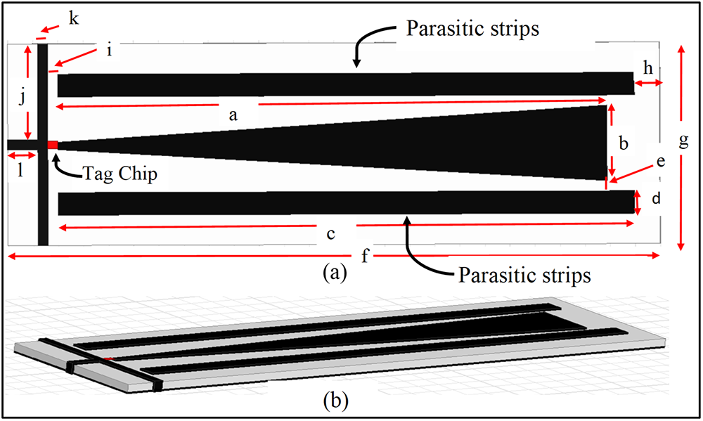
The geometry of the proposed RFID tag is shown in Fig. 1. A triangular patch is designed to increase the bandwidth as the concept reported in papers [Reference Fu, Ren, Yin, Lei and Lian25, Reference Kobayashi and Sawada26]. The tag is fed through narrow grounding strips which exhibits an inductive effect for conjugate impedance matching with tag chip. Two parasitically coupled strips are deigned alongside triangular patch for enhancement in impedance matching and read range at FCC band in simultaneous with ETSI band. The design is placed on Rogers RT/Duroid 5800 grounded dielectric substrate with ε r = 2.2, tanδ = 0.0009 with a thickness of 1.575 mm. The design is simulated using Ansys HFSS tool. The simulated antenna geometry and the associated parameter values are shown in Fig. 1. The optimized dimensions in mm are listed in Table 1.
(a) Top view and (b) side view of the tag antenna geometry.

Optimized design parameters for tag antenna

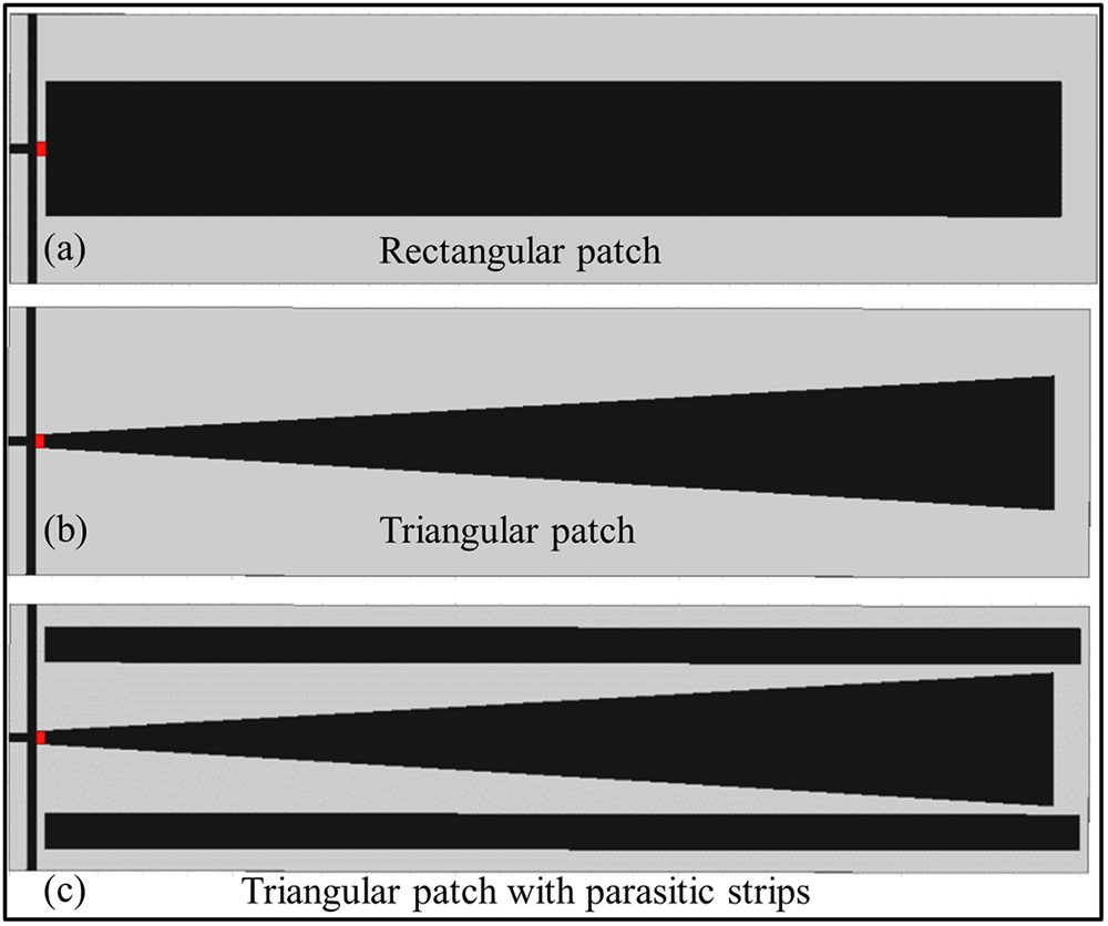
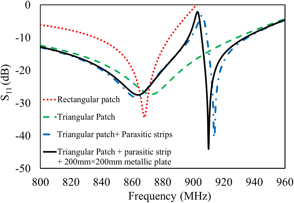
The design of the tag antenna is shown in Fig. 2(a–c). The simulation of the tag antenna is performed in free space environment and on (200 × 200) mm2 metal plate. The simulated S 11 parameters of the antenna are given in Fig. 3. The rectangular patch tag design shown in Fig. 2(a) exhibits very narrow bandwidth of 46 MHz (838–884 MHz) which covers ETSI UHF RFID band (865–868 MHz) only. Further, in order to increase the bandwidth, the antenna is converted into triangular form as shown in Fig. 2(b), the bandwidth gets increases to 160 MHz (770–930 MHz) which covers both ETSI and FCC band as shown in Fig. 3. However, the triangular patch does not provide the good impedance matching in FCC (902–928 MHz). Further, in order to enhance the impedance matching and read range at FCC band, two parasitic strips alongside with triangular patch are designed as shown in Fig. 2(c). The simulation of the tag antenna is performed in free space environment and on (200 × 200) mm2 metal plate. The parasitically coupled strips introduces extra resonating points in the UHF RFID band as shown by simulated responses in Fig. 3, thereby the impedance matching is improved in both ETSI as well as in FCC band [Reference Santiago, Costa and Fernandes28, Reference Lai and Li29].
(a) Tag based on rectangular patch, (b) tag based on triangular patch, and (c) tag based on triangular patch with parasitic strips.

S 11 parameters of the tag antenna in different situation.

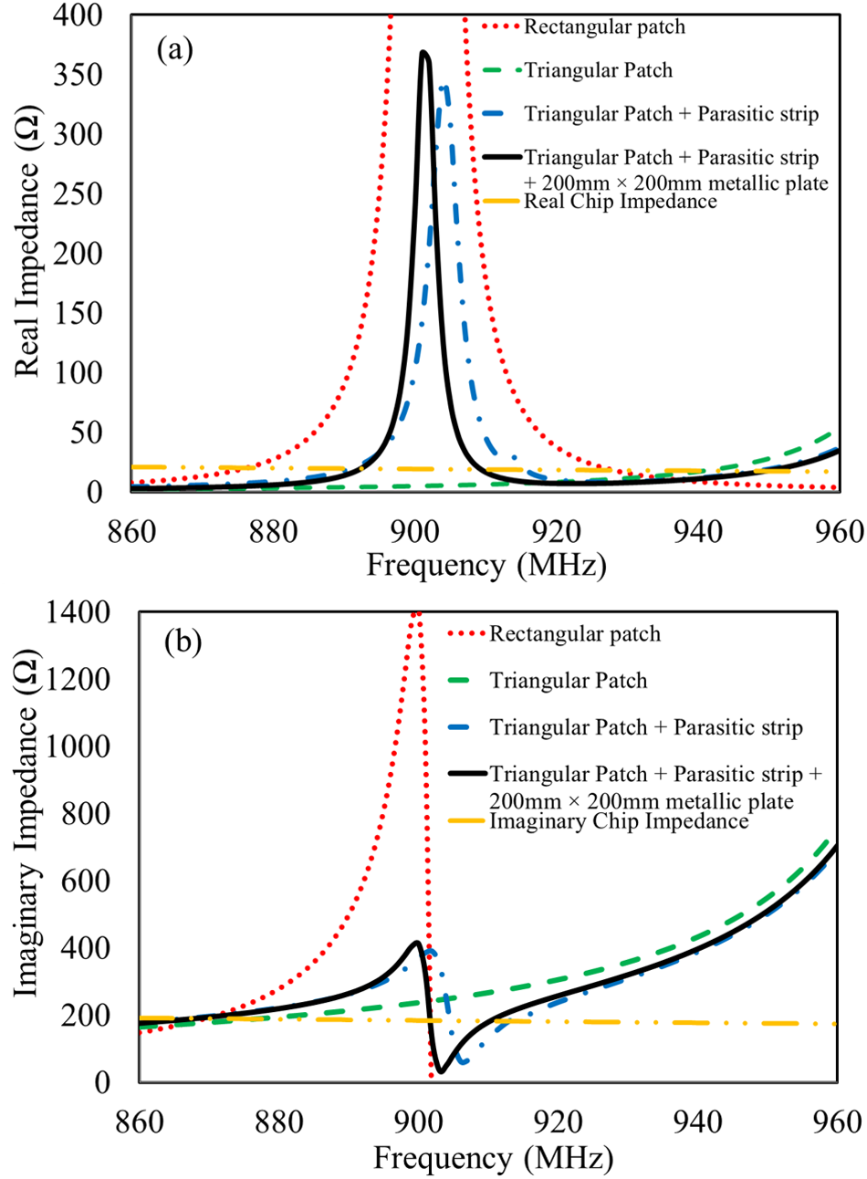
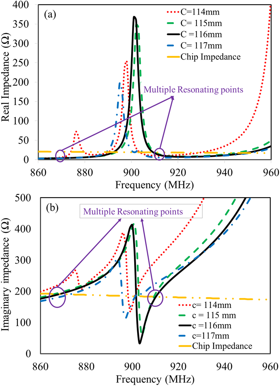
The simulated real and imaginary impedance of the tag antenna is given in Fig. 4(a) and (b), respectively. It is observed that the impedance of the triangular patch is 2.6 + j172.8 Ω at 866 MHz and 6.8 + j277.5 Ω at 913 MHz but the conjugate impedance required to match with that of RFID chip is 20.55 + j191.45 Ω at 866 MHz and 18.65 + j182 Ω at 913 MHz. By inserting the two parasitic strips, the impedance of the tag antenna becomes 5 + j188.7 Ω at 866 MHz and 28 + j182.6 Ω at 913 MHz, which are very close to the imaginary part of the impedance required to match with the impedance of the RFID chip. It is also observed that if the (200 × 200) mm2 metal plate is placed under the RFID tag antenna, the impedance at both the frequencies remains almost same as that of the RFID tag antenna without metal plate. The effect of parasitic strip is studied in Fig. 5. It is observed that if the length of the strip is greater as compared to the length of triangular patch, the design provides multi resonating points. Further, it is observed that when the length “c” is equals to 116 mm, the design exhibits impedance matching points at around 866 MHz and 910 MHz which covers both the European region (ETSI) and the American region (FCC)/Asian region bands. The tag performs almost independently to the use of metal plate as shown in Fig. 3 which makes it capable to use with or without metallic environment.
Z 11 parameters of the tag antenna in different situations.

Effect of parasitic strips on impedance matching at multiple frequency points.

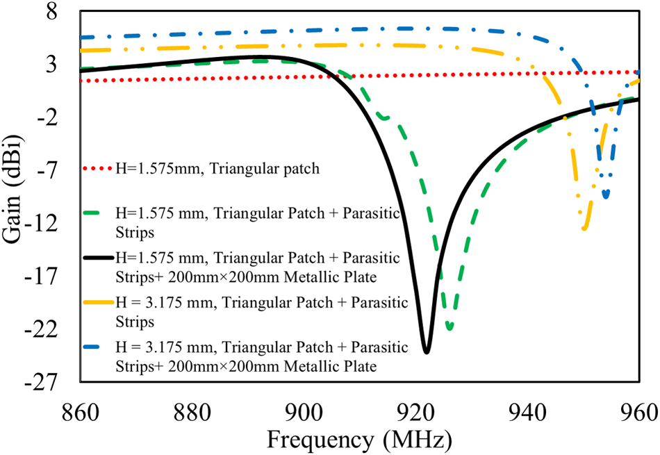
The gain versus frequency curve is shown in Fig. 6. It is observed from curve that the tag antenna design without parasitic strips (only triangular patch) shows almost constant gain in the whole UHF band, but it does not provide multiple impedance matching points in American frequency (FCC) band (902–928 MHz) as shown in Fig. 3. For substrate thickness of 1.575 mm and with parasitic strips the tag antenna provides a maximum gain of around 3 dBi and for 3.175 mm thickness the gain is more than 5.5 dBi in European/Indian (ETSI) band. On the other hand in American (FCC) band, the tag antenna exhibits a gain of around 0 dBi for 1.575 substrate thickness and a gain of 6.5 dBi for 3.175 mm thickness. Hence, as per the requirement, there will be a tradeoff between multiple impedance matching points and required gain in 902–928 MHz frequency band. Further, the design shows almost similar response in free space as well as when placed on (200 × 200) mm2 metallic plate.
Gain vs frequency curve of tag antenna with different substrate thickness (H).

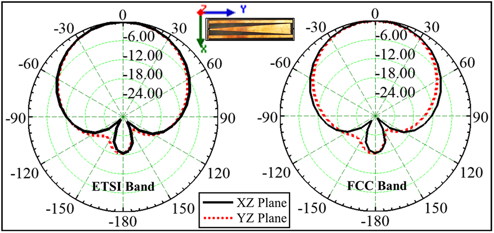
The co- and cross-polar radiation patterns of the respective antennae for different frequencies are shown in Fig. 7. The radiation patterns are observed to be unidirectional at all the frequency which make it suitable for different RF applications.
Simulated results of radiation pattern for the proposed RFID tag.

Tag reading range
The reading range of an RFID tag plays a vital role in improving its use for potential RF applications. Therefore, the performance of the proposed RFID tag in terms of its reading range is also investigated. The maximum range of RFID tag along the (θ, Φ) direction can be calculated by using the Friss transmission equation [Reference Seshagiri Rao, Nikitin and Lam30]
 \begin{equation}{\text{ }}{{\text{d}}_{{\text{max}}}}\left( {\theta {\text{,}}\varphi } \right) = \frac{{\text{c}}}{{4{{\pi f}}}}\sqrt {\frac{{{\text{EIR}}{{\text{P}}_{\text{R}}}}}{{{{\text{P}}_{\text{c}}}}}{{\tau }}{{\text{G}}_{{\text{tag}}}}\left( {{{\theta }},{{\varphi }}} \right)} \end{equation}
where  ${\text{EIR}}{{\text{P}}_{\text{R}}}$ is the effective isotropic radiated power (limited by the radio regulations), given by the product of the transmitted power and the antenna gain
 ${G_{\text{r}}}$ of the reader,
 ${P_{\text{c}}}$ is the minimum threshold RF power required by the chip to turn on and the minimum threshold RF power
 ${P_{\text{c}}}$ for the chip used in this design is −20.5 dBm,
 ${{{G}}_{{\text{tag}}}}\left( {{{\theta }},{{\varphi }}} \right)$ is the gain of the tag antenna, and
 $\tau $ is the power transmission coefficient between the tag antenna and tag chip impedances, where 0 ≤ τ ≤ 1
 \begin{equation}\tau = 1 - \,{\left[ {{\Gamma }} \right]^2} = \frac{{4{Z_{\text{c}}}{Z_{\text{A}}}}}{{{{\left| {{Z_{\text{c}}} + {Z_{\text{A}}}} \right|}^2}}} \leq 1\end{equation}
where “Γ” is the reflection coefficient which accounts for the impedance mismatch between the antenna ( ${Z_{\text{A}}}$) and chip impedance (
 ${Z_{\text{c}}}$)
 \begin{equation}{{\Gamma }} = \frac{{{{\text{Z}}_{\text{c}}}{\text{ }} - {\text{ }}{{\text{Z}}_{\text{A}}}}}{{{{\text{Z}}_{\text{c}}}{\text{ }} + {\text{ }}{{\text{Z}}_{\text{A}}}}}\end{equation}
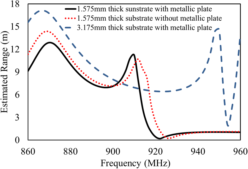
Using the above mentioned equations (1)–(3), the estimated reading ranges of the proposed antenna with different substrate thickness in the entire UHF RFID band are plotted in Fig. 8.
Range vs frequency curve of tag antenna with different substrate thickness (H) for 2 W EIRP.

It is clearly observed from Fig. 8 that the range as well as bandwidth of the tag increases with the increase in the thickness of the substrate. With 3.175 mm thickness, it covers the whole UHF RFID frequency band.
Experimental measurements
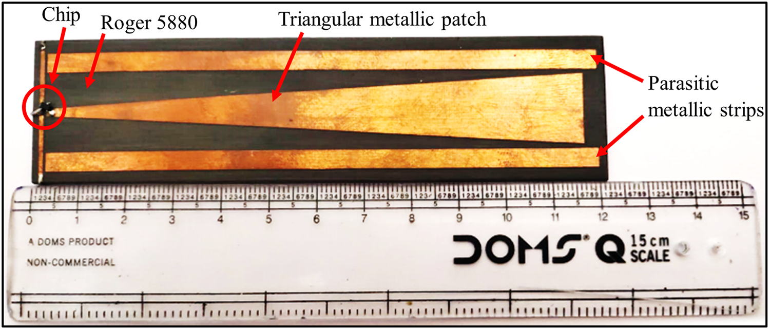
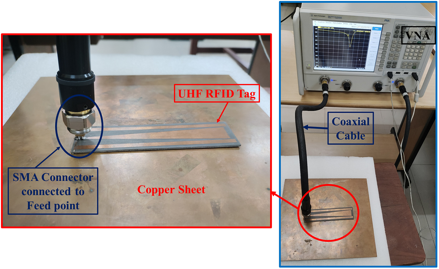
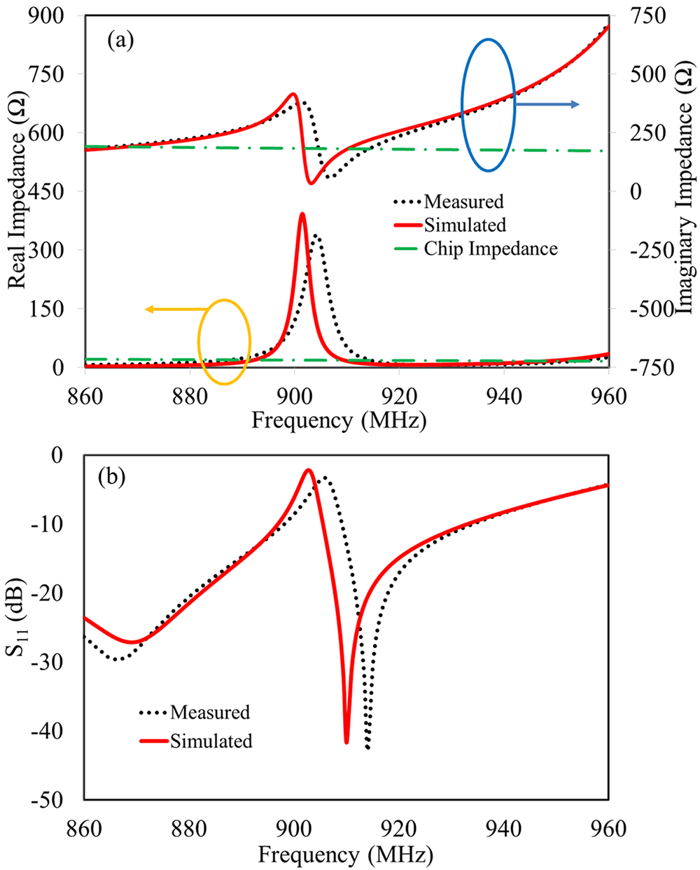
A prototype of RFID tag antenna is fabricated on double side copper plated Rogers RT/Duroid 5880 substrate of thickness 1.575 mm as shown in Fig. 9. The size of the fabricated tag is (121 × 30 × 1.575) mm3. The impedance is measured using vector network analyzer, low loss coaxial cable, and SubMiniature version A (SMA) connector as shown in the measurement setup represented in Fig. 10. The prototype is placed on 20 × 20 cm2 copper sheet. The measured impedance and return loss are shown in Fig. 11(a) and (b), respectively. It is observed that measured responses are quite in agreement with the simulated responses.
Prototype of fabricated RFID tag with chip.

Impedance measurement using vector network analyzer.

Simulated and measured result of UHF RFID tag. (a) Real and imaginary impedance. (b) Return losses S11 in dB.

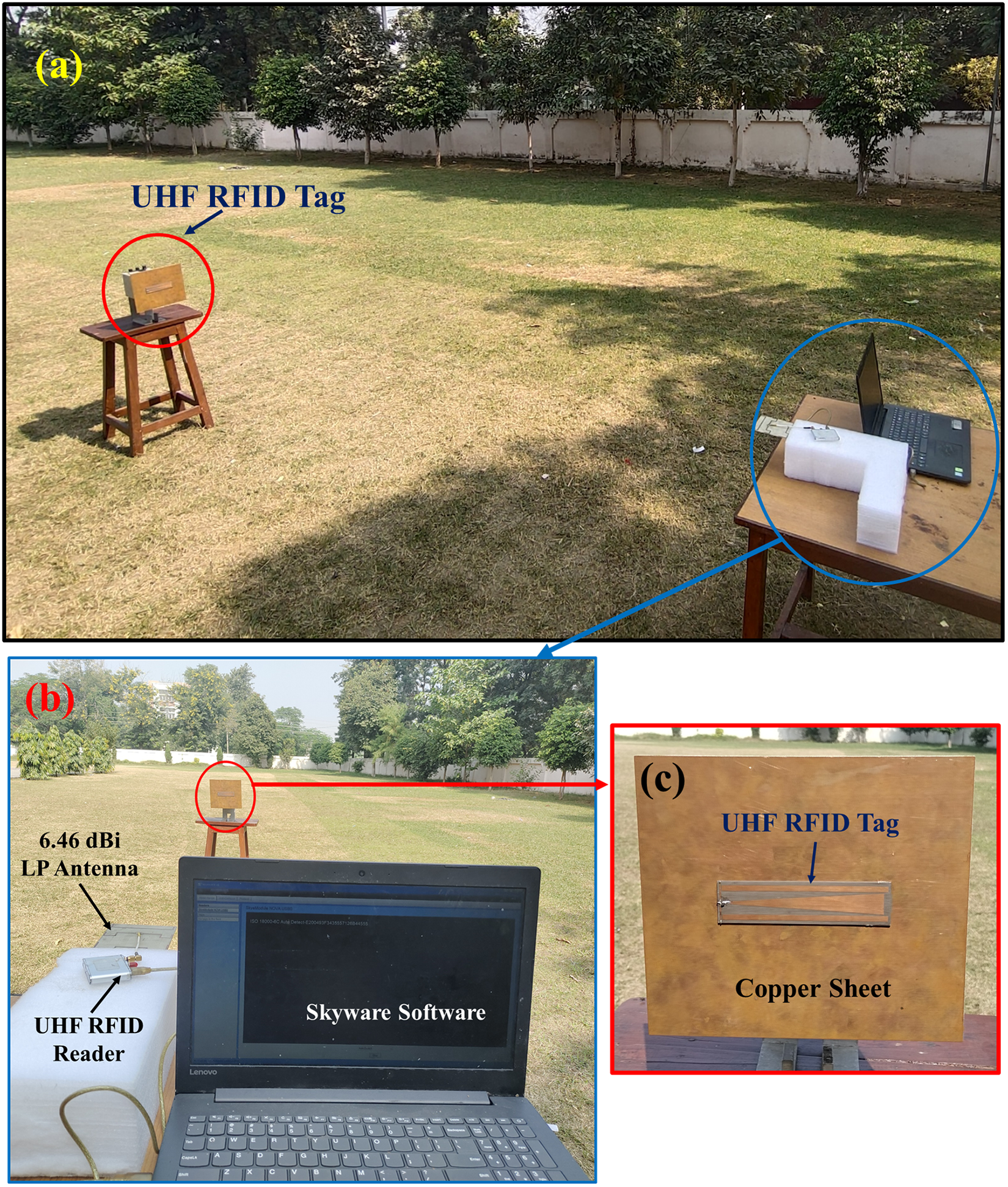
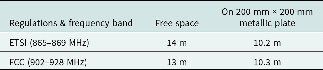
The reading range measurement setup is shown in Fig. 12. The reading range of the tag is measured by using Skyetek Supernova RFID reader [31] connected to a linearly polarized antenna of gain 6.46 dBi as shown in Fig. 12(b). The maximum reading range was measured, by keeping the tag in motion away from the reader along a straight line up to a point where it is maximally detectable for point to point transmission and reception. The read range is tested when the tag is placed on (200 × 200) mm2 metal plate as shown in Fig. 12(c) and in free space. The reading range is measured for the two standard frequency bands that are ETSI (for European countries and India, 866–869 MHz) and FCC (for US, 902–928 MHz). The measured read range for 2 W EIRP of the transmitting source listed in Table 2 and observed in good agreement with the calculated values.
Measurement setup for reading range of the UHF RFID tag. (a) Side view, (b) front view, and (c) UHF RFID tag on copper sheet.

Maximum reading range of tag in two different bands

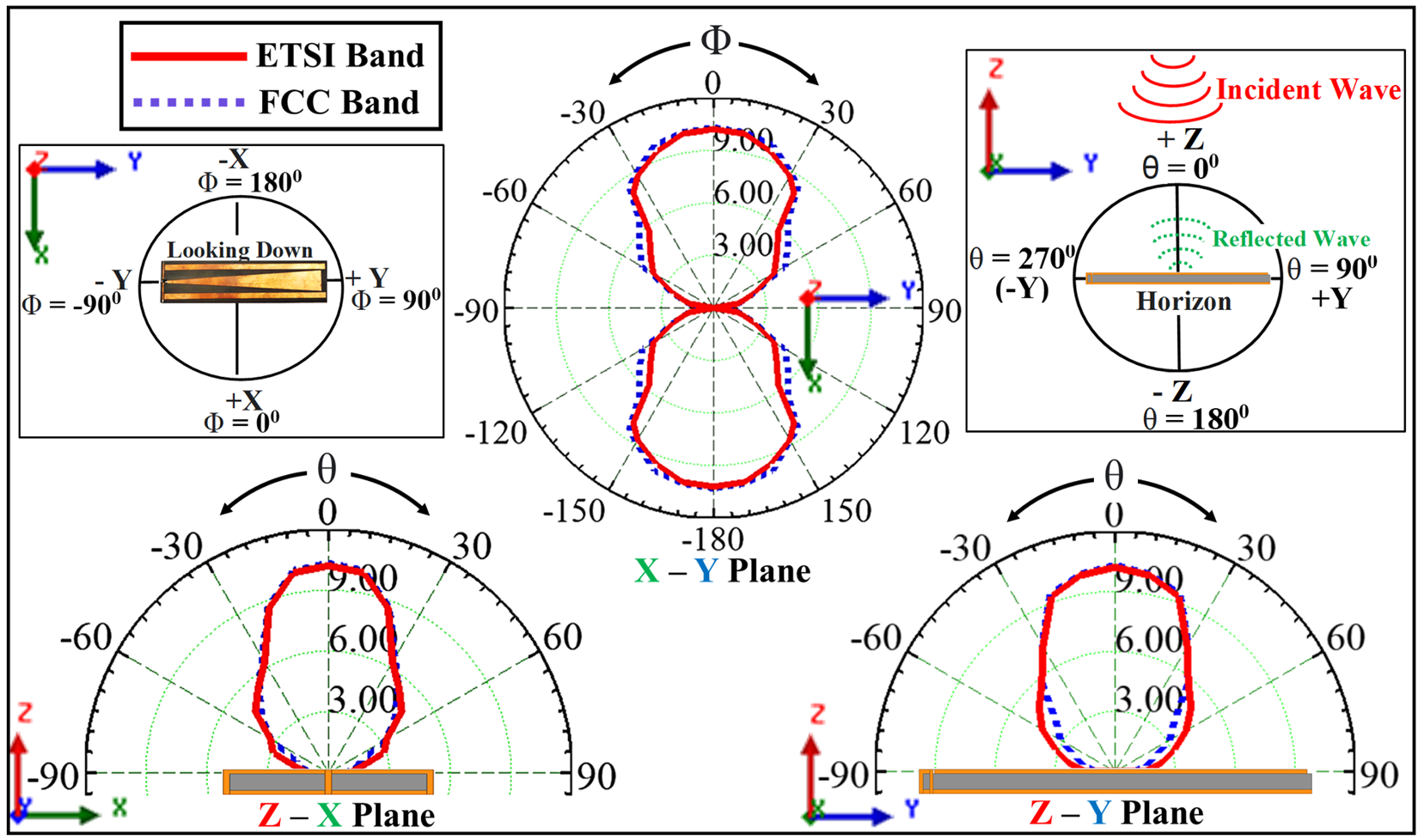
Measurements are conducted by positioning the tag in front of the reader, and additional tests are performed by varying the tag’s orientation in the “θ” and “ɸ” planes to plot its radiation pattern as shown in Fig. 13. In the bore-sight direction (θ = 0°), the reading range is 10.2 m for the ETSI band and 10.3 m for the FCC band. However, as “ɸ” increases, the reading range decreases in the X–Y plane due to reduced polarization efficiency. At ɸ = 90°, the reading range drops to nearly zero meters because the electric field of the tag antenna is perpendicular to the electric field of the linearly polarized transmitting reader antenna. Furthermore, as “θ” increases, the reading range also diminishes in the Z–X and Z–Y planes, which is due to the continuous copper plane at the back of the tag antenna. At “θ” = 180°, the reading range is reduced to zero.
Measured radiation pattern in XY, ZX (ɸ = 0°), and ZY (ɸ = 90°) plane.

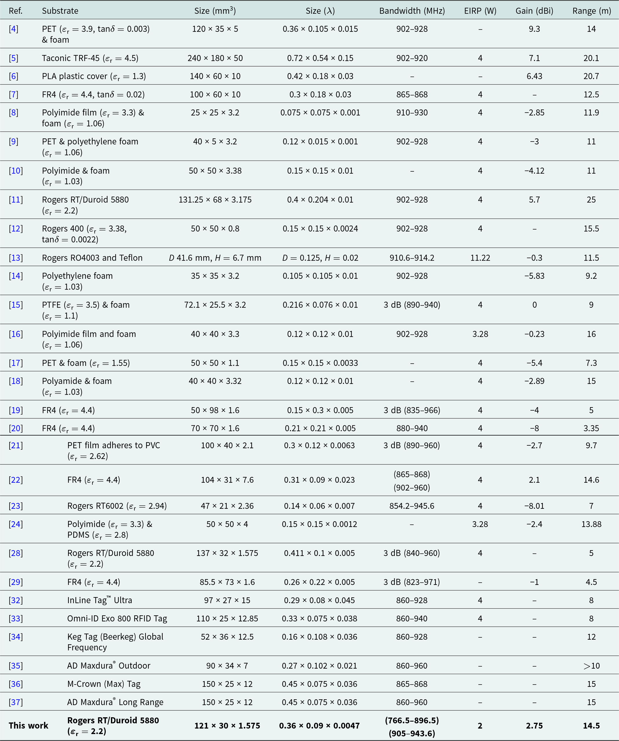
The proposed tag antenna has been compared to previously reported RFID tags in terms of antenna size, bandwidth, gain, substrate thickness, and reading range, as shown in Table 3. It is observed that the −10 dB bandwidth and reading range of the proposed tag antenna are better than those reported in papers [Reference Park, Lee and Park4–Reference Son, Jeon and Cho21]. Although the bandwidth in paper [Reference Hamani, Yagoub, Vuong and Touhami22] is comparatively good, the substrate thickness is greater and the gain is lower compared to this work. In paper [Reference Hamani, Yagoub, Vuong and Touhami22], the reader’s emitted power was set to 3.3 W EIRP for the European band (ETSI) and 4 W EIRP for the American (FCC) and Asian bands, achieving a maximum read range of 11.8 m at 868 MHz and 14.6 m at 905 MHz. In this work, the reader’s output power is set to 2 W EIRP for both the European and American bands, providing a maximum read range of 10.2 m in the European (ETSI)/Indian band and 9 m in the American (FCC) band with a substrate thickness of 1.575 mm. The designs in papers [Reference Santiago, Costa and Fernandes28] and [Reference Lai and Li29] offer good bandwidth but have a larger footprint and provide a shorter reading range. Additionally, the tags reported in papers [Reference Kim and Yeo5, Reference Byondi, Sul and Chung6], and [Reference Björninen, Delzo, Ukkonen, Elsherbeni and Sydänheimo11] achieve a long reading range but are larger in size and offer less bandwidth. The designs in papers [Reference Paredes, Zamora, Nguyen, Martín and Bonache12, Reference Alagiasundaram, Lee, Lim, Chee and Bong16], and [Reference Murugesh, Lim, Chee and Bong18] exhibit comparable reading range performance with compact sizes but are limited to a single frequency band. The proposed tag is also compared with commercially available UHF RFID tags [32–37]. It provides better performance than papers [32] and [33] with reduced thickness. The tags in papers [34] and [35] show comparable performance, though they are thicker than the proposed tag. Further, papers [36] and [37] deliver slightly better performance than the proposed tag but have larger overall dimensions. Thus, the compact size of (121 × 30 × 1.575) mm3dimensions, wide bandwidth, and long reading range of up to 10.2 m for both ETSI (865–868 MHz) and FCC (902–928 MHz) bands over the metal surfaces of the proposed UHF RFID tag makes it a potential candidate to serve applications such as asset tracking, factory automation, and inventory management. For example, in order to monitor metal containers, tools, and machinery in industrial environments, the designed tag can be attached to above mentioned items, and the tag antenna transmits the item’s unique identification number to RFID readers. This enables real-time tracking of inventory levels in warehouses, retail stores, or distribution centers. Its robust design on a rigid substrate ensures durability and reliable performance under harsh environmental conditions.
Performance comparison with published works

Conclusion
In this paper, a novel compact RFID tag with broadband characteristics is designed and characterized. The tag is fabricated on a Rogers RT/Duroid 5880 grounded substrate, it covers the major portion of the UHF RFID band with −10 dB return loss. The overall size of the tag is (121 × 30 × 1.575) mm3. Triangular patch is used to enhance the impedance matching bandwidth between the antenna and tag chip without any additional matching networks. The parasitic strips are used to provide the multi resonating points so that it is capable to provide good performance in both ETSI as well as FCC bands. The performance of the tag is studied for different thickness of the substrate used in the design of the tag. The performance of the proposed tag is verified by measuring its reading range in free space as well as on 200 × 200 mm2 metal plate to make it useful for potential RF applications such as supply chain, asset tracking, waste management like industrial bin identification, bicycle or ports equipment, packaging and labels, clothing and apparel, metal pallet tracking, oil and gas industry, aerospace and aviation, shipping container tracking, railway coaches identification, etc. The reading range of the fabricated tags is measured for the frequency band of different countries. The tag exhibit maximum reading range of (14 m in free space and 10.2 m on metallic plate) in ETSI (865–869 MHz) band and reading range of (13 m in free space and 10.3 m on metallic plate) for FCC band (902–928 MHz).
Competing interests
We declare that there are no conflicts of interest, financial or otherwise, related to the research presented in this manuscript. I have not received any financial support or funding from any private or governmental organizations or individuals in relation to this work.

Abhishek Choudhary received his B.Tech (ECE) degree in 2013 and M.Tech. degree in Electronics and Communication Engineering from University Institute of Engineering and Technology (UIET), Kurukshetra University, Kurukshetra, Haryana, India, in 2015. He is currently pursuing his Ph.D. from UIET, Kurukshetra University, Kurukshetra. His research interests include antennas, tags, and reader antenna design for RFID applications.

Dr. Deepak Sood has received his Ph.D. from Kurukshetra University, Kurukshetra, Haryana, India, in the year 2016, M.Tech (ECE) in 2007 and B.Tech (ECE) degree in 2002. He is currently working as an assistant professor in the Department of Electronics & Communication Engineering of UIET, Kurukshetra University, Kurukshetra, Haryana, India. He has 21 years of teaching experience. He has more than 40 research papers at national and international level in various fields of RF engineering. His research interests include design and development of metamaterial-based microwave absorbers, development of spatial filters using frequency selective surfaces, RFID, microstrip-based RF device design such as hybrid network, power divider, directional coupler, filters, and antenna design.