I. INTRODUCTION
There is a need for simple and reliable sensors that are suitable for trace detection in a spectrum of applications ranging from medical diagnosis, environmental monitoring, industrial and agricultural process control, and lab-on-a-chip. Reference Mao, Chang, Zhou and Chen1,Reference Zhang and Lieber2 In the past two decades, various nanomaterials have been explored for sensing applications, including quantum dots, Reference Freeman, Finder, Gill and Willner3–Reference Li, Wang, Wang, Tang, Pounds and Lin5 nanoparticles, Reference Lang, Fu, Hou, Han, Yang, Liu and Jiang6–Reference Zhao, Hilliard, Mechery, Wang, Bagwe, Jin and Tan8 nanowires, Reference Cui, Wei, Park and Lieber9–Reference Zheng, Patolsky, Cui, Wang and Lieber11 carbon nanotubes, Reference Allen, Kichambare and Star12–Reference Star, Gabriel, Bradley and Gruner14 and graphene. Reference Liu, Dong and Chen15–Reference Zhan, Li, Yang, Jenkins, Huang and Dong17 Among these nanomaterials, graphene, a two-dimensional (2D) carbon layer, has drawn significant attention in sensor applications due to its unique structure and properties. Graphene has demonstrated great potential in various novel sensors (optical, electronic, electrochemical, and mechanical sensors) due to its exceptional optical properties, electronic properties, electrochemical properties, or mechanical properties. Reference Mao, Chang, Zhou and Chen1,Reference Liu, Dong and Chen15,Reference Yang, Ratinac, Ringer, Thordarson, Gooding and Braet16,Reference Chang, Mao, Zhang, Cui, Zhou, Wu, Yang and Chen18–Reference Mao, Lu and Chen20
For electronic field-effect transistor (FET) biosensors, the unique structure and electronic properties of graphene, e.g., ultra-thin thickness, large specific surface area, extremely high electron mobility, and high sensitivity to electronic perturbations from foreign molecules, are the cornerstones for the use of graphene-based materials as the sensing material. The general working principle of graphene-based FET sensors is based on the conductivity change in the sensing channel (graphene nanosheet) upon the binding of target biomolecules. Reference Zhan, Li, Yang, Jenkins, Huang and Dong17,Reference He, Wu, Yin and Zhang21 To make this binding event specific, probes are usually labeled on the graphene sheet surface through surface modification (chemical or physical linkage) and act as the binding sites for target biomolecules. Reference Zhan, Li, Yang, Jenkins, Huang and Dong17,Reference He, Wu, Yin and Zhang21 In the sensing step, when a target biomolecule binds to the probe, it causes a change in the electrical conductance of the graphene nanosheet that can be measured by the external circuit/measuring system. Through proper calibration, graphene-based FET sensors can be used for quantitative measurements of biomolecules, and a good low limit of detection (LOD) is achieved due to the high sensitivity of graphene to electronic perturbations from foreign biomolecules. In addition to the good LOD, compared with optical biosensors, the test procedure of FET sensor is simple and no chemical reagents are needed for the detection. Moreover, FET sensor normally has rapid response with a detection time on the order of seconds. These properties make the FET sensor an ideal candidate for rapid detection of biomolecules with low concentrations or real-time monitoring/online detection of biomolecules. So far, many studies have demonstrated the use of graphene FET sensors in detecting biomolecules, including DNA, protein (antibody, biomarker, and glucose), and bacteria. Reference Chen, Chen, Huang, Selegard, Platt, Palaniappan, Aili, Tok and Liedberg22–Reference Zhu, Du and Lin25
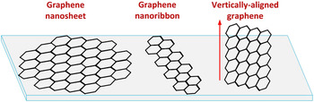
The performance of graphene FET biosensors largely depends on the sensor structure and the properties of the sensing material and probe. To explore the potential of graphene-based sensors, three graphene structures have been studied in FET sensors: graphene nanosheet, graphene nanoribbon (GNR), and vertically aligned graphene (as shown in Fig. 1). Graphene or reduced graphene oxide (RGO) nanosheets, the most commonly used material in graphene FET sensors, have been demonstrated in various sensing platforms for detecting biomolecules. Reference Zhan, Li, Yang, Jenkins, Huang and Dong17,Reference He, Wu, Yin and Zhang21 As an alternative to graphene nanosheet, GNR has drawn great attention in FET sensors due to its large band gap, which could potentially lead to higher sensor sensitivity. Reference Dong, Long, Wang, Chan-Park, Huang, Huang and Chen26,Reference Tan, Chuang, Lin, Zhou and Cheng27 Vertically-aligned graphene (VG) is an emerging graphene structure that has a vertically aligned nanosheet structure on a substrate. The major advantages of VG in FET sensors is its unique vertical orientation and open structure. Reference Bo, Mao, Han, Cen, Chen and Ostrikov28 This article will review and discuss recent progress in graphene nanosheet, GNR, and VG-based FET sensors. Insights are given for the future development of graphene-based FET sensors for real biomedical applications.
Schematics of graphene nanosheet, GNR, and vertically aligned graphene structures.

II. GRAPHENE-BASED FET BIOSENSORS
A. Graphene nanosheet biosensors
The first graphene-based FET sensor was reported in 2007 by Novoselov’s group, which demonstrated that micrometer-size sensors made from graphene were capable of detecting individual gas molecules that attach to or detach from the graphene surface. Reference Schedin, Geim, Morozov, Hill, Blake, Katsnelson and Novoselov29 The group showed that the adsorbed molecules change the local carrier concentration in graphene one electron by one electron, which leads to step-wise changes in conductivity. This study opened the door for a new type of FET sensor based on the 2D graphene nanosheet. Since then, many studies have focused on graphene-based sensors and have shown that graphene is sensitive to changes in its chemical environment due to its high specific surface area, high carrier mobility, and low electrical noise at room temperature. Reference Robinson, Perkins, Snow, Wei and Sheehan30
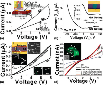
The first study using a graphene FET device for detecting biomolecules was reported by Mohanty et al. in 2008, Reference Mohanty and Berry31 in which the group fabricated a graphene FET device and studied its interactions with single bacterium and DNA. To study the graphene interaction with bacteria, the graphene sheet was functionalized with amine groups [graphene-amine (GA)]. To construct an FET sensor, gold electrodes were patterned on a Si wafer with an open channel. For conductivity (drain-source current versus drain-source voltage) and transistor (drain-source current versus gate voltage) measurements, the sensing material or sensing channel, in this case, the graphene nanosheet, bridged the electrodes and a top or back gate potential was applied to the device. The electrical measurements of GO and GA sheets are shown in Figs. 2(a) and 2(b), in which the silicon as a backgate was used to determine the semiconductor characteristics of the materials. The results showed that both GO and GA exhibited a slightly nonlinear current–voltage behavior in dry nitrogen atmosphere, and the GA device had a lower conductivity than the parent GO device. Mohanty et al. also found that the surface modification of GO sheet could change its conductivity due to the change in the carrier density and mobility of the nanosheet. Both the GO and GA devices were p-type semiconductors (a doped semiconductor contains mostly free holes as the carrier), which is typical for GO and RGO FET devices.
(a) The current–voltage (I–V) curves of the GO and GA devices. The insets show the device with GO/GA between gold electrodes and a schematic of the GO and GA’s chemical structure. (b) FET curves of GO and GA show they are p-type semiconductors. The top inset shows the post-deposited gold electrodes on a GO sheet. (c) The conductivity of the p-type GA device increases upon attachment of a single bacterial cell on the surface of GA (inset 1). LIVE/DEAD confocal microscopy test on the bacteria deposited on GA (insets 2–4). (d) DNA transistor: ss-DNA tethering on GO increases the conductivity of the device. Inset shows a G-DNA(ds) sheet with wrinkles and folds clearly visible. Reproduced with permission. Reference Mohanty and Berry31 Copyright 2008, American Chemical Society.

Bacterium attachment on a GA device was characterized with the I–V test, as shown in Fig. 2(c). The GA device exhibited a sharp 42% increase in conductivity upon the attachment of a single bacterial cell (Gram-positive Bacillus cereus cell). This could be attributed to the p-type characteristic of GA, where the attachment of a negatively charged species such as bacteria, is equivalent to a negative potential gating, which increases the hole density and thus the conductivity of GA (gating effect). Applying a similar idea, they also studied the interaction of the GO device with DNA. At first, selective tethering of the single-stranded DNA (probe DNA, 2.5 μg/μL) on GO to form G-DNA was carried out, and, subsequently, hybridization with cDNA (target DNA, 0.175 μg/μL) was conducted on the G-DNA device. The second step led to a 71% increase in conductivity [Fig. 2(d)]. Since the probe and target DNA pair is specific, a highly selective sensor could be designed. The results from this study showed the possibility of using graphene nanostructures as a bacteria cell or as a label-free DNA detector.
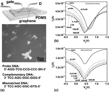
After the first report on the electrical detection of DNA hybridization by monitoring the conductance change of GO sheets, many studies were carried out to further evaluate the potential of using a graphene FET device to detect DNA. Reference Dong, Shi, Huang, Chen and Li32–Reference Ping, Vishnubhotla, Vrudhula and Johnson37 In 2010, Dong et al. reported label-free and sensitive DNA detection using graphene-based FET devices. Reference Dong, Shi, Huang, Chen and Li32 The major innovation in this study is that the detection was based on the Dirac point shift in the transistor measurement. Dong et al. fabricated their graphene FET devices using chemical vapor deposition (CVD)-grown graphene sheets with probe DNA pre-immobilized on the surface of graphene film. Figure 3(a) shows a schematic of the graphene device, which is operated by a liquid gating. The typical transistor curve shown in Fig. 3(b) demonstrates that the graphene device exhibited ambipolar behaviors subjecting to the gate voltage applied to the bath solution. The gate voltage (V g) that gave the minimum graphene conductance (Dirac point) could be identified from the transfer curve and used to monitor the doping state of the graphene film. Figure 3(b) also shows that the Dirac point was sensitive to the immobilization of probe DNA and the hybridization of the complementary target DNA. Specifically, after hybridization with target DNA, the Dirac point significantly left-shifted with the addition of DNA molecules, suggesting that DNA molecules n-doped the graphene film. In this study, Dong et al. tested the mismatched DNA with the device and the results [Fig. 3(c)] showed that the mismatched DNA had an insignificant impact on the Dirac point. These results proved that the large shift in the Dirac point was caused by the complementary DNA, not the nonspecific binding between the complementary DNA and graphene. To increase the loading density of probe DNA, Dong et al. proposed a method using Au nanoparticles (NPs) as a linker to anchor the thiolated probe DNA molecule to the graphene surface. Their sensors showed a detection limit of 0.01 nM and a sensing range of 0.01–500 nM. As we discussed, gating effect and doping effect are two commonly accepted sensing mechanisms for graphene FET sensors. For this study, Dong et al. proposed that the n-doping effect played an important role for the electrical detection of DNA. Based on the two reports on graphene FET DNA sensor, it is found that both conductivity (I–V) and transistor (Dirac point shift) measurements could be used to investigate the DNA binding event; and the I–V measurement is actually the measurement of current change in the sensor when the gate potential is fixed at 0 V. The I–V detection is easier for the quantification of signal and the transistor measurement is useful to understand the sensing mechanism.
(a) Schematic illustration of the graphene device operated by liquid gating. Middle is an optical microscopy image of the graphene films. Bottom shows the DNA sequences used in the experiments. Transfer characteristics for the graphene transistors before adding DNA, after immobilization with probe DNA, and after reaction with (b) complementary or (c) one-base mismatched DNA molecules with the concentration ranging from 0.01 to 500 nM. Reproduced with permission. Reference Dong, Shi, Huang, Chen and Li32 Copyright 2010, John Wiley & Sons, Inc.

In addition to Au NPs, other metal nanoparticles, such as Pt NPs, were used as the linker for probe immobilization on the graphene sheet surface. Reference Yin, He, Huang, Zhang, Wu, Chen, Lu, Chen, Zhang, Yan and Zhang34 For real application of the DNA sensor, one target is to develop ultra-sensitive sensors that can detect low-concentration DNA samples. Recently, an RGO-based FET biosensor was reported for ultra-sensitive label-free detection of DNA via peptide nucleic acid (PNA)–DNA hybridization. Reference Cai, Wang, Huang, Ning, Zhang and Zhang36 In this study, PNA was used as the probe instead of DNA, and DNA detection was performed through PNA–DNA hybridization. The sensor’s detection limit was achieved at 100 fM level. It was reported that the sensitivity of DNA biosensors depended on the length of the oligomer. In one study, a CVD-grown graphene FET sensor was reported for 60-mer, 40-mer, and 22-mer DNA detection. Their results showed that 60-mer DNA had the lowest LOD of 1 fM, and the LODs for 40-mer and 20-mer DNA were 100 fM and 100 pM, respectively. Reference Ping, Vishnubhotla, Vrudhula and Johnson37
DNA detection was demonstrated with graphene FET sensors, and the detection of other biological molecules, such as protein, was reported using graphene sensors. Reference Ohno, Maehashi, Yamashiro and Matsumoto38–Reference Piccinini, Bliem, Reiner-Rozman, Battaglini, Azzaroni and Knoll47 In 2009, Ohno et al. first reported the electrolyte-gated graphene FET device for detecting bovine serum albumin (BSA). Reference Ohno, Maehashi, Yamashiro and Matsumoto38 Without any surface modification on the graphene sheet, BSA was prepared with phosphate buffer electrolyte solution at pH 6.8 and injected onto the graphene surface. The dynamic measurement of conductance versus time for various BSA concentrations suggested that the conductance of the graphene FET increased with the addition of BSA. Based on the conductivity change, the adsorption of BSA on the graphene surface was confirmed. The FET sensor response was attributed to the gating effect from BSA molecules, which are negatively charged at the pH used for their measurement. Although this sensor device might have low selectivity to BSA, since no specific probe was used to differentiate BSA from other proteins, this study again confirmed that the surface charge on the biomolecule could change the conductivity of graphene when the biomolecule was attached to its surface.
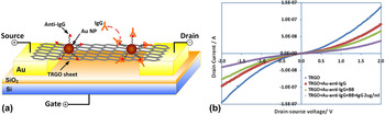
Soon after the report of the first graphene FET protein sensor, Chen group reported a thermally-reduced GO (TRGO) sensor for specific detection of immunoglobulin G (IgG). Reference Mao, Lu, Yu, Bo and Chen48 Thermal annealing is one of most commonly used methods for GO reduction since the reduction level could be easily controlled by adjusting the reduction temperature and the RGO nanosheet has a relatively high purity compared with chemical reduction method. This study presents a methodology for avoiding nonspecific protein immobilization on TRGO while at the same time providing a stable binding for probe proteins through robust Au NPs. A schematic of the TRGO FET device is shown in Fig. 4(a), in which the TRGO sheet was suspended above the substrate across the gold electrodes. Anti-Immunoglobulin G (anti-IgG) was anchored to the TRGO surface and functioned as the specific recognition group for the IgG binding. To link the anti-IgG to TRGO nanosheet, at first, the antibody was linked to the Au NP through a chemical linker (thiol chemistry), then the antibody–NP conjugates were deposited onto the RGO nanosheet and the NP attached to RGO nanosheet through Van der Waals force. A blocking buffer (BB) was used to prevent possible nonspecific binding events. Figure 4(b) shows the evolution of drain current (I d) when the TRGO FET device was treated with Au NP–anti-IgG conjugates, BB, and IgG (2 μg/mL). With the introduction of the target protein, a significant decrease in the I d was observed due to the binding of IgG to anti-IgG. This protein sensor had a detection limit of 2 ng/mL and showed negligible responses to mismatched proteins such as Immunoglobulin M (IgM) and horseradish peroxidase (HRP). Soon after this study, Chen group further investigated the dependence of the sensor response on the TRGO base resistance and the antibody areal density on the TRGO sheet. Reference Mao, Yu, Lu and Chen49 A correlation of the sensor response with sensor parameters was found. The sensor response was more significant with larger TRGO base resistance (depending on the alignment and density of TRGO sheets on the electrodes) and higher antibody areal density. With an optimized sensor structure, the detection limit of the TRGO FET sensor was improved to 0.2 ng/mL level.
(a) Schematic of a TRGO FET. Anti-IgG is anchored to the TRGO sheet surface with Au NPs and functions as a specific recognition group for the IgG binding. (b) Evolution of drain–source voltage dependence of the drain current I d when the TRGO FET device is treated with Au NP–anti-IgG conjugates, BB, and IgG (2 μg/mL). Reproduced with permission. Reference Mao, Lu, Yu, Bo and Chen48 Copyright 2010, John Wiley & Sons, Inc.

In addition, biotin–streptavidin protein detection was demonstrated with a three-dimensional (3D) graphene FET platform. Reference Kim, Sohn, Lee, Han, Lee, Jung and Lee50 In this platform, vertically aligned ZnO nanorods as a sensing surface, capped by an ultra-thin TiO2 layer for improved electrolytic stability, were grown on a CVD graphene channel. The sensor showed a rapid detection capability with a very fast response time (∼1 min) to proteins with an fM-level concentration. This is attributed to the fast binding kinetics of the probe-target proteins, the small diffusion length of the target molecules to reach the sensor surface, and the large density of available probe molecules on the vertical ZnO nanorods.
Another application of graphene FET sensors is cancer biomarker detection. One report demonstrated RGO FET biosensors for label-free detection of a prostate cancer biomarker, prostate specific antigen/α1-antichymotrypsin (PSA–ACT). Reference Kim, Sohn, Jung, Yoon, Lee and Park45 The immunoreaction of PSA–ACT complexes with PSA monoclonal antibodies on the RGO channel surface led to a linear response in the shift of the Dirac point in the transistor curve. The RGO FET could detect protein–protein interactions down to the femtomolar level (LOD at 1.1 fM) and it showed a high specificity to other cancer biomarkers in the PBS solutions, as well as in the human serum.
Many studies have shown that graphene FET devices are highly sensitive to pH change in aqueous solution. Reference Ohno, Maehashi, Yamashiro and Matsumoto38,Reference Kwon, Yi, Lee, Shin, Kim, Cho, Nam and Park51 Using this idea, Her et al. developed a graphene FET sensor to detect alanine aminotransferase (ALT), which is an enzyme that can be used in combination with other enzymes to diagnose the course of various liver disorders. Reference Her, Pan, Lin, Wang and Li52 The FET device exhibited a high pH sensitivity of 23.12 mV/pH (Dirac point shift). The sensor could accurately determine the variation in pH, which is related to the generation of H+ ions during the enzymatic reaction between biocomponents of l-alanine, α-ketoglutarate, and ALT. This type of biosensor exhibited a linear response toward the ALT concentrations in the range from 10 to 100 U/L, with an evaluated detection sensitivity of 0.42 mV/(U/L).
Blood glucose monitoring is a way of testing the concentration of glucose in the blood (glycemia), which is particularly important in the care of diabetes mellitus. As demonstrated, graphene nanosheet is highly sensitive to biomolecule attachment Reference Ghoshdastider, Wu, Trzaskowski, Mlynarczyk, Miszta, Gurusaran, Viswanathan, Renugopalakrishnan and Filipek53 and thus graphene FET devices also have been demonstrated for sensing glucose. Reference Huang, Dong, Shi, Li, Li and Chen54–Reference Zhang, Liao, Mak, You, Mak and Yan57 In a representative study, the Chen group reported the redox enzyme-modified graphene devices for real-time detection of glucose and glutamate. Reference Huang, Dong, Shi, Li, Li and Chen54 The working principle of this sensor was based on the conductance change of the graphene transistor as the glucose molecules were oxidized by the specific redox enzyme [glucose oxidase (GOD)] functionalized on the graphene film.
As shown in Fig. 5(a), GOD was immobilized onto graphene film via a linker molecule (1-pyrenebutanoic acid succinimidyl ester), with one end attached to the graphene surface through π–π interaction with a pyrene group, and the other end covalently reacted with the amino group on the enzyme by an amide bond. GOD catalyzed the oxidation of glucose in the following reaction: β-D-glucose + O2 + H2O → D-glucono-1,5-lactone + H2O2. The sensor response to this reaction is shown in Fig. 5(b). An obvious increase of I ds was observed when glucose was added to the testing chamber filled with PBS solution. I ds increased as more glucose was added, and the graphene response tended to saturate at glucose concentrations larger than 10 mM [Fig. 5(b)] due to the limited density of GODs on the graphene film and/or the limited reaction rate of GOD. Using the same platform, the Chen group also demonstrated the detection of glutamate molecules with glutamic dehydrogenase enzyme. The detection limit of the graphene FET glucose sensor (0.1 mM) was comparable to the commonly used electrochemical sensors. After this study, zinc oxide NPs-decorated graphene film Reference Kavitha, Gopalan, Lee and Park58 and a flexible graphene device [graphene on polyethylene terephthalate (PET) substrate] Reference Kwak, Choi, Kim, Kim, Yoon, Ahn, Yang, Yang and Seo55 were reported for sensing glucose and showed promising performance compared with electrochemical glucose sensors. Given their perfect 2D structure, excellent electronic properties, and the ability to support cell adhesion, graphene FET devices also promise applications that interface with living cells/bacteria and monitor their dynamic activities. Reference Ang, Li, Jaiswal, Wang, Hou, Thong, Lim and Loh59–Reference Mannoor, Tao, Clayton, Sengupta, Kaplan, Naik, Verma, Omenetto and McAlpine61
(a) Schematic illustration of GOD-functionalized graphene FET. (b) Current responses to the addition of glucose at various concentrations. The upper inset shows that GOD-free graphene FET is not responsive to 10 mM glucose. The lower inset shows the response curve of the graphene FET to glucose fitted by an exponential function. Reproduced with permission. Reference Huang, Dong, Shi, Li, Li and Chen54 Copyright 2010, The Royal Society of Chemistry.

B. GNR biosensors
As we know, intrinsic graphene has a zero band gap and exhibits a low on–off current ratio when used as the conducting channel in an FET, which largely limits its application in electronic sensors. There are methods to convert graphene from a semimetal to a semiconductor. In particular, a sizable energy gap can be opened up in graphene through the quantum confinement effect by engineering graphene in the form of a GNR or a graphene nanomesh. Reference Lu, Yu, Wen and Chen62 FET sensors based on a single GNR are anticipated to have high sensitivity and high spatial resolution. Reference Tamersit and Djeffal63 A theoretical study on a GNR-based DNA sequencing device showed that when a single-stranded DNA (ssDNA) was electrophoretically threaded through the GNR channel, the electrical signatures of four types of nucleotides could be measured, which indicated the high sensitivity of the GNR to biomolecule interactions. Reference Min, Kim, Cho and Kim64
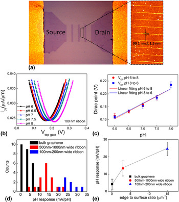
GNR could be made by electron beam lithography (EBL) and oxygen plasma treatments on pristine graphene nanosheets. GNR FET sensors fabricated by this method were reported for pH measurement. Reference Tan, Chuang, Lin, Zhou and Cheng27 As shown in Fig. 6(a), the graphene FET sensor, consisting of GNR arrays patterned by EBL and oxygen plasma, has four columns of ribbons connected with large graphene islands. Each GNR was measured to be 99.1 ± 1.5 nm wide, 5.5 μm long, and 1–2 layers thick. Figure 6(b) shows the transfer curves of a GNR device in different pH solutions. The transfer curves were identical in different pH solutions, but the Dirac point shifted to positive potential with a higher pH. The sensor sensitivity was ∼23.6 mV/pH: this strong response could be attributed to the dangling bonds associated with GNR edges. Figure 6(c) shows the Dirac point position versus pH (pH changes from 6 to 8 and then back to 6), from which a linear relation was obtained. In this study, the authors compared the pH responses of the sensors with different graphene structures, i.e., pristine graphene, wide GNRs with a width of 500–1000 nm, and narrow GNR with a width of 100–200 nm [Figs. 6(d) and 6(e)]. The results revealed that the pH response increases when the GNR width decreases. The improved pH response in GNR is attributed to the increased number of hydroxyl groups attached to edge defects, as the edge-length-to-surface-area ratio increases when the GNR width decreases. It is found that the shift of the Dirac point in response to the pH change was reversible, indicating the hydroxyl ions are binding to the edge defect sites through physical adsorption.
(a) Microscopic image of graphene FET after EBL edge patterning (left); AFM image to show GNRs (right). (b) Drain-source current density I ds (current was normalized to the width of the graphene channel) as a function of the top gate potential V g in different pH buffer solutions for FET made of 100 nm-wide GNRs. (c) Dirac point shift in response to the different pH. (d) Histogram of sensitivity for the FETs with pristine graphene and graphene ribbons of various widths, pH response of different devices (mV/pH). (e) Average pH response with different edge-to-surface-area ratio. Reproduced with permission. Reference Tan, Chuang, Lin, Zhou and Cheng27 Copyright 2013, American Chemical Society.

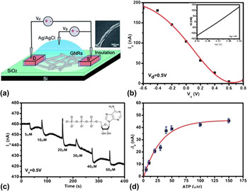
In another study, Dong et al. reported a reduced graphene oxide nanoribbon (rGONR) sensor made by chemically unzipping multiwalled carbon nanotubes (MWCNTs). Reference Dong, Long, Wang, Chan-Park, Huang, Huang and Chen26 To investigate the electrical properties of the rGONR thin-film network, a liquid-gated field-effect transistor was constructed [Fig. 7(a)]. The transistor properties of a typical rGONR device (source–drain current versus gate voltage) is shown in Fig. 7(b). The on–off ratio of the prepared rGONR thin-film is ∼52.0 ± 8.6 (n = 10 devices), which is much larger than the typical on–off ratio (<3) of graphene nanosheet or rGO. Reference Lu, Yu, Wen and Chen62,Reference Mao, Yu, Cui, Bo, Lu and Chen65 As shown in Figs. 7(c) and 7(d), the addition of adenosine triphosphate (ATP) molecules decreased the conductance of the rGONR film and the detection limit was achieved at 5 µM. Based on the electrostatic gating effect from the highly negatively charged ATP molecules, the sensor should have increased conductivity upon ATP binding; however, the experimental results showed that the sensor conductivity decreased. To understand the sensing mechanism, Dong et al. measured the I d–V g curve of the rGONR device before and after the addition of ATP. It was found that ATP changed the rGONR conductivity through an n-doping effect, and the current on–off ratio of the sensor greatly decreased after ATP binding.
(a) Schematic illustration of the rGONR thin-film network device configured as a liquid-gated FET with phosphate buffer saline solution as the electrolyte. (b) I d–V g curve of a typical rGONR FET biased at V d = 0.5 V. The inset shows the I d–V g curve at V g = 0 V for the same device. (c) Real-time recording of the I d of a typical rGONR thin-film device in PBS, at V d = 0.5 V and V g = 0 V. The inset shows the molecular structure of ATP. (d) The current response versus ATP concentration (n = 3 devices; the error bars indicate the standard deviation). Reproduced with permission. Reference Dong, Long, Wang, Chan-Park, Huang, Huang and Chen26 Copyright 2011, The Royal Society of Chemistry.

It is believed that the improvement in graphene semiconducting properties by structure engineering will be an appealing direction for the future development of graphene-based FET sensors. However, one of the major challenges in GNR FET sensors is nanoribbon fabrication. To make the sensor more applicable, a simple and low-cost fabrication method for large-scale production of GNR is needed. Compared with EBL, oxygen plasma treatments, and chemically unzipping CNT, a low-cost and facile shrink lithography method was used to form suspended GNR FET sensors for pH and cancer marker sensing applications. Reference Zhang and Cui66 A 50 nm wide GNR was fabricated and used for detecting prostate-specific antigen, which achieved an LOD of 0.4 pg/mL.
C. Vertically-aligned graphene biosensors
Although graphene FET devices show promise in miniaturized and high-performance sensors, many challenges still remain for the low-cost and large-scale fabrication of graphene sensors with reliable performance. Recently, vertically-oriented graphene (VG) has emerged as a new type of graphene material. Due to VG’s unique structure and properties, VG-based nanostructures have been explored to advance sensing technology. Reference Bo, Mao, Han, Cen, Chen and Ostrikov28 Using VG as the sensing element, VG sensors have been studied for detecting biomolecules (e.g., protein) Reference Mao, Yu, Chang, Steeber, Ocola and Chen67 and gases (e.g., NO2, NH3, and H2). Reference Seo, Rider, Kumar, Randeniya and Ostrikou68–Reference Yu, Wang, Lu, Chen, Bo and Chen70 Different from conventional graphene, VG draws increasing attention in biosensor applications due to its unique vertical orientation and open structure. VG is a high-performing sensing material, as its surface can be fully accessible by analytes, and the high length of exposed edges and the high in-plane carrier mobility lead to superior sensor performance.
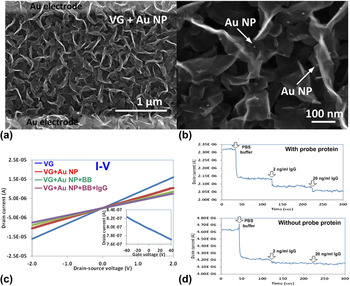
VG-based FET biosensors were reported for protein detection. Reference Mao, Yu, Chang, Steeber, Ocola and Chen67 As shown in Figs. 8(a) and 8(b), VG as the sensing material was directly grown on the sensor electrodes using the plasma-enhanced chemical vapor deposition (PECVD) method. Au NP–antibody conjugates as a probe for analyte protein binding were deposited on the VG surface, which allowed the direct diffusion and binding of the target protein (IgG) to the probe protein (anti-IgG) on the Au NP. In this sensor, the VG showed p-type semiconducting characteristics in an ambient environment, which is quite similar to the characteristics of graphene or RGO. During the sensing test [Fig. 8(c)], with the IgG sample added to the sensor, the drain current I d decreased and the sensor had a high sensitivity to antibody and antigen interactions.
(a) SEM image of VG network between electrode fingers after deposition with Au NP–antibody conjugates. (b) Magnified SEM image of VG network deposited with Au NP–antibody conjugates. (c) Sensor conductivity changes with probe antibody labeling and analyte protein detection. Inset is the FET transport characteristic of the VG. (d) Dynamic responses of the VG sensor exposed to different concentrations of IgG with (top) and without (bottom) probe proteins. Reprinted with permission. Reference Mao, Yu, Chang, Steeber, Ocola and Chen67 Copyright 2013 Macmillan Publishers Limited.

Graphene-based FET sensors normally have a rapid response to target analytes, which offer great potential for using the sensors in real-time biosensing and rapid diagnostics. Figure 8(d) shows the dynamic responses of VG sensors to different IgG concentrations with and without the probe proteins, respectively. The results showed that the sensor conductivity decreased correspondingly with the injection of the IgG, and the response time was on the order of seconds. The critical function of the probe in the sensor was confirmed, since the sensors without probes showed much lower responses than those with probes. By comparing the VG sensor with conventional horizontal graphene-based sensors, the vertical orientation and open structure of VG increase the accessible area of the device to the analytes, thereby increasing the sensitivity of the sensor. In addition, the direct PECVD growth of VG on sensor electrodes could achieve higher stability and reproducibility than the drop-casting method commonly used in graphene sensor fabrication. The high stability and reproducibility are believed to be due to the strong binding between the VG and the sensor electrode.
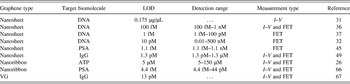
Table I summarizes the performance of representative graphene nanosheet, GNR, and VG FET biosensors. The graphene FET sensors have been demonstrated for various types of biomolecules detection including DNA, protein, and bacterium. I–V and FET are two commonly used measurement types in detection, which utilized current change and Dirac point shift as the sensing signal, respectively. Based on the studies shown in Table I, the LOD of the sensors is achieved at an extremely low level of fM, which is superior to commonly used optical methods.
Graphene nanosheet, GNR, and VG FET biosensors. I–V represents for drain–source current and drain–source voltage measurement, and FET represents for transistor (Dirac point shift) measurement.

III. CONCLUSION AND FUTURE DIRECTIONS
In this article, representative graphene-based FET sensors are reviewed for biosensing applications. Shortly after its discovery, graphene has been explored in a variety of biosensing applications due to its exceptional electrical properties and unique structures. Compared with 1D semiconducting nanowires and nanotubes, graphene has shown superior performance and great potential for biological sensors. Compared with conventional biosensing techniques, graphene-based biosensors have tremendous advantages, such as high sensitivity and selectivity, fast response, easy operation with simple instruments, and relatively low cost, and could be ideal candidates for the next generation of biosensors. Although some promise is envisioned, graphene-based commercial biosensors are yet to come and there is still a need for breakthroughs in sensor research either for improving the sensor performance or for lowering the sensor cost and developing more adoptable sensor fabrication methods.
In laboratory demonstrations, the performance of some reported graphene FET sensors could meet the need for practical applications; however, when the sensors are fabricated at a large scale, degradation in the sensor performance and quality is very common. The qualities of graphene-based sensor, e.g., reproducibility, long-term stability, and false control, represents great challenges for real applications or commercialization of the sensor. Among these challenges, the reproducibility or reliability of the sensor needs much attention. To improve the sensor’s reproducibility, sensor device fabrication should be precisely controlled to minimize the device-to-device variations, e.g., graphene sheet density on the electrode and probe density on the graphene sheet. To this direction, advancements in fabrication methods, e.g., printing method and use of thickness and shape controlled graphene film, are highly needed for the device fabrication. Research is also needed to develop cost-effective and scalable production methods that can retain the essential properties of graphene materials and minimize the device-to-device variations. Second, a calibration method should be developed to precisely correlate the sensor sensitivity to biomolecule concentration. In the calibration, sensor electrical characteristics, e.g., initial resistance and transistor on–off current ratio, should be taken into consideration.
For the future direction of graphene-based FET sensors, improvement in the sensor performance, i.e., sensitivity and selectivity, is foreseen by engineering the graphene/probe hybrid structure. On the other hand, the sensor platform design and signal acquisition system could be further developed for easy signal acquisition, higher signal to noise ratio, and large sample size statistical analysis. Reference Basu and RoyChaudhuri71,Reference Mackin and Palacios72 Recycling of the sensor for multiple-time use also worth study, especially when the sensor is used for long-term continuous detection. With the development of manufacturing method and sensor structure design, graphene FET biosensors have a great potential to assist or replace existing optical sensors in the future.