Introduction
In the last 20 years, with the growth of wired networks and mobile communication systems, numerous wireless access technologies have been progressed. Latterly, with the growth of smart gadgets like home digital entertainment center, the need for a high transmission rate in wireless technology has fascinated extensive attention. It has been proved that improved data rate can be attained by combining ultra-wideband (UWB) with multiple inputs multiple outputs (MIMO) systems [Reference Sim, Chung and Lee1]. UWB systems operate from 3.1 to 10.6 GHz, comprise channel capacity, eliminate the fading effect, etc. Therefore, by employing UWB MIMO systems, the fading effect and data rate can be further improved without passive elements. Presently, many researchers mainly focus on miniaturization, broadband, high isolation that improves the enactment of UWB MIMO antennas. Numerous methods developed in the literature to have enhanced impedance matching with compact size. These techniques are multi-session transformers, tapered lines, and distributed impedance matching [Reference Negi2]. Multi-session transformer method is the modified version of the quarter-wave transformer, employing multiple segments of λ/4 transmission lines linked together [Reference Negi2]. The disadvantage of this technique is that it makes the system complex. In the tapered line technique, the feed line width is exponentially increased or decreased for the impedance matching purpose. Another technique is distributed impedance matching where the structure is modified itself without using any passive element for widening the impedance bandwidth. Other than impedance bandwidth, UWB systems require a band-notched filter to suppress the interference from the narrowband system, such as WiMAX varies from 3.3 to 3.7 GHz, WLAN varies from 5 to 6 GHz, and X-band system varies from 7.2 to 8.4 GHz; therefore, UWB systems do not cause any interference to the other existing narrowband systems [Reference Thakur, Jaglan, Gupta and Kanaujia3]. Numerous designs are discussed in the literature such as etch slots of different shapes such as open-end quarter wavelength rectangular slot [Reference Gujral, Li, Yuan and Qiu4], arc [Reference Xie, Zhao, Jiao and Zhang5], meandered in the patch surface or on the ground surface. Another method to achieve band notch characteristics is by adding stub [Reference Guichi, Challal and Denidni6] and parasitic element beside the feed line and rejection resonators like capacitively-loaded loop [Reference Zitouni and Hacene7]. The above-discussed method produces poor radiation patterns due to perturbation in the radiating surface or on the ground plane. Lately, multiple band notches are attained by using single electromagnetic band gap (EBG) structures. In [Reference Jaglan, Gupta, Thakur, Kumar, Kanaujia and Srivastava8], three bands are rejected by using three different EBG structures. In [Reference Liu and Xu9], two EBG structures obtain three rejected bands at three interfering narrow bands. Further in [Reference Ghosh, Mandal and Das10], a single EBG structure obtains triple notches with a size of 9.4 × 4.5 mm2.
Triple notch UWB MIMO antenna
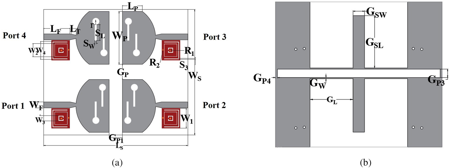
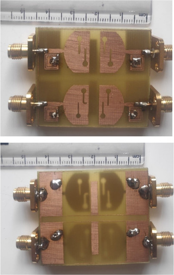
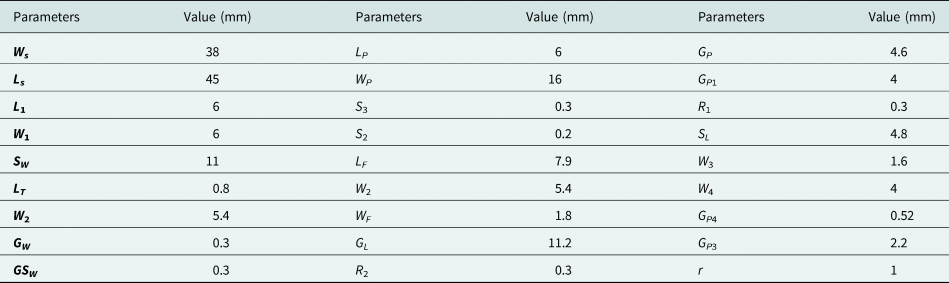
The final prototype of the structure is depicted in Fig. 1 and the adjusted parameters of the suggested antenna are presented in Table 1. HFSS (v13) is used to design and simulate the suggested antenna. For validation, the proposed antenna is fabricated using the EP 2006 PCB prototype machine. This four-element UWB antenna is fabricated using FR-4 having ɛr of 4.4 and has a compact size of 38 × 43 × 1.6 mm3. Figure 2 presents the prototype of the proposed UWB MIMO antenna. The S-parameters are measured using the Agilent N5230C vector network analyzer, and gain and radiation patterns are tested using the microwave shield anechoic chamber, respectively. The values of SL, SW, WP, LP, and LT are varied to get a wider bandwidth of 9 GHz (2–11 GHz), which covers the entire frequency range. To generate triple notches, the EBG structure is placed near the feedline of the suggested antenna.
(a) Layout of the top view of suggested antenna. (b) Layout of the bottom view of suggested antenna.

Prototype of the proposed four-element UWB MIMO antenna.

Dimensions of the suggested structure

Band gap determination
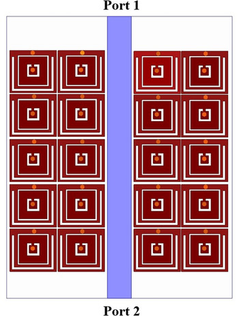
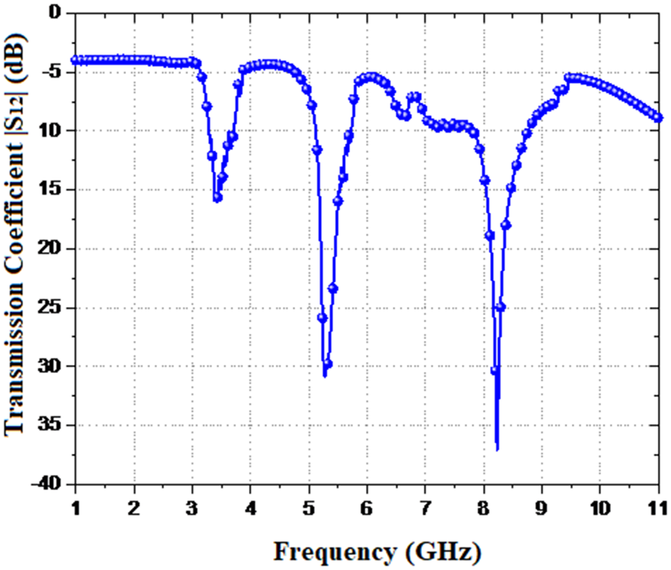
To further validate the band gap characteristic of EBG structure, the proposed EBG structure 5 × 4 lattice of EBG structure is simulated using an FR4 substrate with ɛr = 4.4 with the height of 1.6 mm. The bandwidth of the band gap of the EBG structure is computed by using the suspended microstrip transmission line method presented in Fig. 3. In the presence of the EBG periodic structure, the transmission responses (S 21) between the two ports are analyzed to obtain the band gap properties. Figure 4 shows three band gaps as 0.4 GHz (3.3–3.7 GHz), 1 GHz (5.15–5.85 GHz), and 1.4 GHz (7.2–8.6 GHz); the minimum S 21 value is about −37 dB for the triple band gaps.
Transmission line over modified EBG structure.

Transmission coefficient for modified EBG structure.

Equivalent circuit model
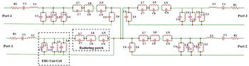
The equivalent circuit of the suggested structure is depicted in Fig. 5. The arrangement of inductor (L), capacitor (C), and resistance (R) is used to demonstrate the port of 50 Ω load, feed line, and radiating patch [Reference Malviya, Panigrahi and Kartikeyan11]. The fed lines and radiating patch are symbolized by the series and parallel arrangement of L1, C1, R1, and L7, C7… LN, CN, respectively. The parallel arrangement of L6 and C6 use to denote the mutual coupling among ports 1–2, and ports 1–4. Similarly, the parallel arrangement of L5 and C5 is used to symbolize isolation between ports 1–3. The modified EBG structure is equivalent to three resonant circuits denoted by parallel combination L2 and C2, L3 and C3, and L4 and C4.
Equivalent circuit.

Numerical results and discussion
Voltage standing wave ratio (VSWR) and S parameters
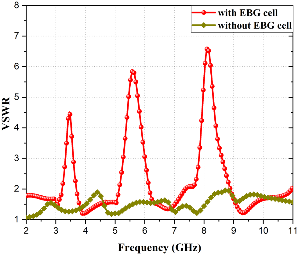
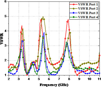
Figure 6 illustrates the simulated VSWR curve with and without the EBG structure. From the simulated result, it is observed that the UWB MIMO antenna with EBG structure function in the entire UWB range except for WiMAX, WLAN, and X-band. The VSWR parameter of the suggested antenna is illustrated in Fig. 7 and it show that the VSWR value at rejecting bands is more than 2; therefore, it is clear that no radiation is taking place at the rejecting frequencies 3.5, 5.5, and 7.7 GHz.
Deviation of VSWR with frequency.

Variation of VSWR with the frequency of different ports.

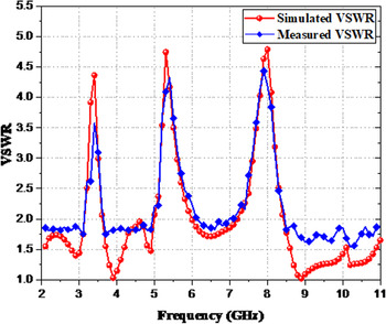
However, Fig. 8 shows the tested and simulated VSWR curve of the structure. The difference in the tested and simulated results is because of the various losses like conduction loss, dielectric loss, mismatch loss, SubMiniature version A (SMA) soldering, fabrication error, measurement error, and orientation problems when the proposed structure is connected to the vector network analyzer [Reference Thakur, Jaglan and Gupta12].
Variation of measured and simulated VSWR.

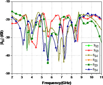
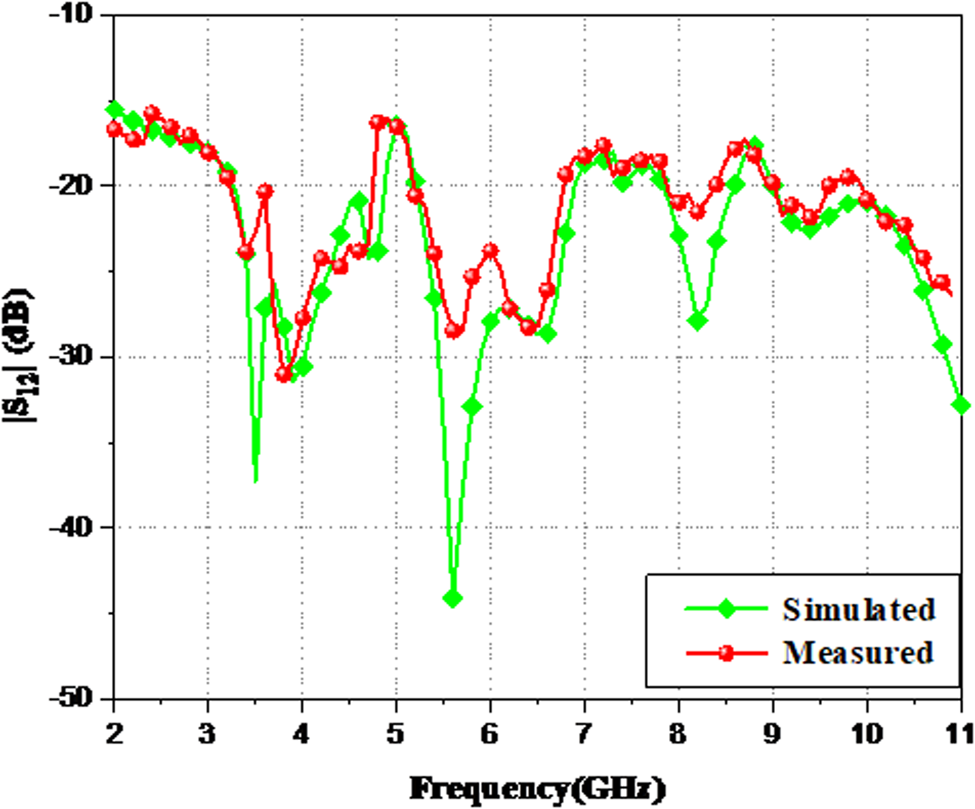
Figure 9 demonstrates the isolation of the suggested antenna. The mutual coupling among the patch antenna is considerably minimized by using T-shaped stubs on the ground plane. A slot is etched on the ground plane to enhance the isolation. It can be seen from Fig. 10 that mutual coupling is below −15 dB for the whole frequency band. The measured curves confirm good resemblance with simulated curves.
Deviation of mutual coupling with frequency.

Variation of mutual coupling with frequency.

Radiation pattern
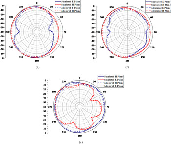
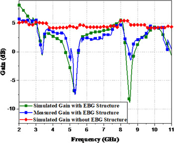
Figure 11 indicates the simulated and tested radiation plot at 4, 6.3, and 7.6 GHz at both E plane and H plane. It is seen that the suggested structure shows a ring-shaped radiation pattern in the H plane and rotation symmetry at the E plane. Figure 12 illustrates that the gain of the suggested antenna is varied from −9.5 to 7.5 dB for the entire UWB range.
(a) Normalized radiation plot at 4 GHz. (b) Normalized radiation plot at 6.3 GHz. (c) Normalized radiation plot at 7.6 GHz.

Deviation of gain with frequency.

MIMO characteristics
The significant factors to analyze and validate the MIMO characteristics are envelope correlation coefficient (ECC), diversity gain (DG), total active reflection coefficient (TARC) [Reference Chae, Oh and Park13], and mean effective gain (MEG) [Reference Karaboikis, Papamichael, Tsachtsiris, Soras and Makios14]. During the analysis of the MIMO antenna, the ECC is considered as a valuable parameter to evaluate the degree of signal fading or diversity skill of the MIMO antenna. Correlation is commonly used to measure the difference between the radiation patterns. ECC and DG can be determined using S parameters [Reference Chae, Oh and Park13] and radiation pattern [Reference Karaboikis, Papamichael, Tsachtsiris, Soras and Makios14]. The mathematical formula to evaluate the ECC in terms of scattering parameters and radiations pattern can be given by [Reference Chandel, Gautam and Rambabu15]

For four elements:


where S 11, S 22, S 33, and S 44 are the reflection coefficients. S 12, S 21, S 31, S 13, S 41, and S 14 are coupling between the ports:

XPR is the cross-polarization rate of the incident field:

where PV and PH are the average power along elevation (θ) and azimuthal angle (ϕ). DG is an efficient parameter used to measure the enactment level of diversity systems. The DG defined as the slant of the error probability plot of the received SNR DG is related to ECC by the below equation [Reference Kumar, Kumar, Kumar Vishwakarma and Srivastava16]

The RE and BW of an MIMO antenna are not accurately characterized by return loss. Therefore, rather than using return loss, TARC can be used so that it accounts for both coupling and random signal combination. Thus, TARC delivers a more significant measure of MIMO efficiency.
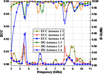
Figure 13 shows the simulated ECC and DG measured using S parameters. Ideally, ECC must be 0 but practically it should be beneath 0.5 and DG must be around 10 dB. The ECC and DG for different antenna elements are within 0.02 and 9.92 dB, respectively. The radiation efficiency and bandwidth of an MIMO antenna are not accurately characterized by return loss. Therefore, rather than using return loss, TARC can be used so that it accounts for both coupling and random signal combination. TARC is a significant factor that denotes the mutual coupling of the ports. For the four-port UWB MIMO antenna, the TARC can be calculated using below equation [Reference Blanch, Romeu and Corbella17]:

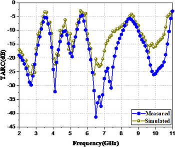
Figure 14 illustrates the TARC of the suggested antenna. Ideally, for an MIMO system, the TARC should be less than 0 dB. It is clear from Fig. 14 that the TARC is below −2.5 dB for the complete band with the triple rejected bands.
Deviation of ECC and DG with frequency.

Variation of TARC with frequency.

MEG is one of the significant factors and is defined as the relation given below [Reference Tang, Zhan, Wu, Xu, Chen and Hu18]:

where N is the number of patches and μirad is the efficiency. In this case N = 4:


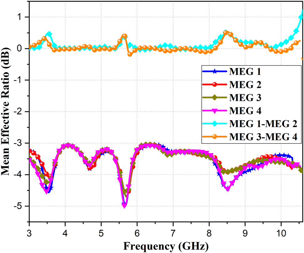
For better diversity performance, the range of MEG should be |MEG i − MEG j| < −3 dB. The simulated MEG of the suggested four-port UWB MIMO is shown in Fig. 15. The value of MEG's for all the four elements is within the desired limit. The performance evaluation of the suggested UWB MIMO antenna with those recent antennas in the publication is presented in Table 2.
Variation of MEG with frequency.

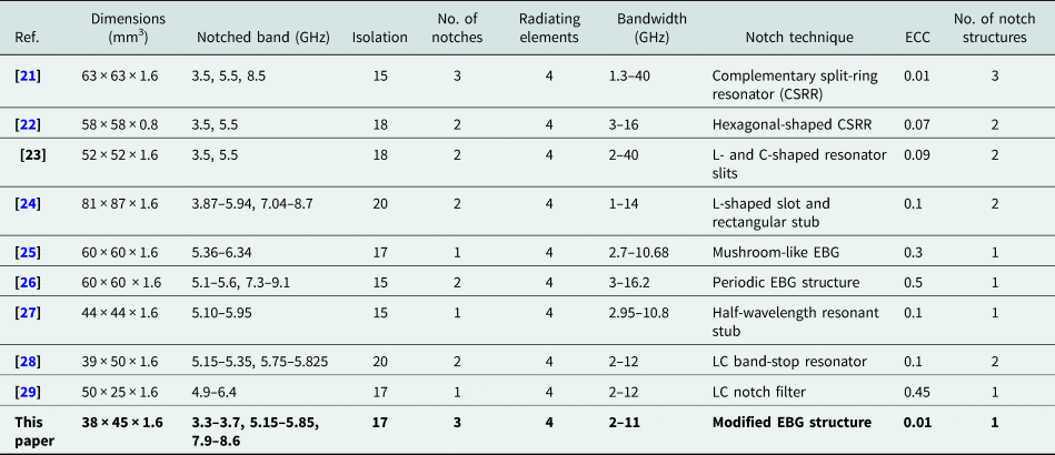
Comparison table of the proposed antenna with other antennas

Performance comparison of different antennas
Table 2 shows the comparative study of different four-element band-notched UWB antennas. Size of the antenna, number of notches, bandwidth, number of notch structures, and ECC [Reference Dastranj19, Reference Amin, Saleem, Shabbir, ur Rehman, Bilal and Shafique20] are some of the important parameters considered for the comparison. It can be observed from Table 2 that notch structures given in [Reference Kumar, Urooj and Alrowais21–Reference Kiem, Phuong and Chien25, Reference Liu and Tu27–Reference Khan, Naqvi, Iftikhar, Asif, Fida and Shubair29] provide notches at a single frequency. EBG structures given in [Reference Wu, Yuan and Wu26] provide notches at two different frequencies. The proposed antenna has compact size, better ECC, and precise notches at three different interfering bands. The proposed antenna provides triple-band notch characteristics using a single EBG structure with better diversity characteristics. Therefore, the proposed antenna can be used as a suitable design for modern wireless communication systems.
Conclusion
In this paper, a miniaturized band-rejected UWB MIMO antenna is designed. A modified EBG unit cell is used to obtain three band-notched characteristics. The novelty of this structure is that the three rejection bands are obtained by using only a modified compact EBG structure with C-shaped slots on its surface. A single EBG structure is used instead of using multiple EBG structures. The tested and simulated scattering parameters, gain, mutual coupling, and radiation patterns were studied and tested. The proposed antenna attains decent diversity performance parameters with ECC < 0.02, TARC < −7.5 dB, and MEG is in the desired limits. The measured result shows a good resemblance.
 Ekta Thakur received her B.Tech. degree in Electronics and Communication Engineering from Bahra University and her M.Tech. degree in Electronics and Communication Engineering from the Jaypee University of Information Technology, Solan in 2016. She obtained her Ph.D. degree on “Design and development of compact MIMO/diversity band notched UWB antennas” from the Jaypee University of Information Technology, Solan in December 2020. Her main research interests include, ultra-wideband antennas, band notched antennas, meta-materials, MIMO systems, electromagnetic band gap structures, and circular polarized UWB antennas.
 Naveen Jaglan was born in 1989. He obtained hid B.Tech (Hons.) and M.Tech (Hons.) degrees in Electronics and Communication Engineering from Kurukshetra University, Kurukshetra, India in 2009 and 2011, respectively. He obtained his Ph.D. on “Design and development of microstrip antennas integrated with electromagnetic band gap structures” from the Jaypee Institute of Information Technology, Sec-62, Noida, U.P., India in June 2017. He has authored/co-authored several research papers in referred international journals and conferences. His research has included microwave communications, 5G antenna design, planar and conformal microstrip antennas including array mutual coupling, artificial materials (metamorphic and metamaterials), EBG, PBG, FSS, DGS, novel antennas, UWB antennas, MIMO systems, numerical methods in electromagnetics, composite right/left handed (CRLH) transmissions and high-k dielectrics. His skill includes modeling of antenna and RF circuits with Ansoft HFSS/CST Microwave Studio/ADS Momentum, measurements using vector network analyzer and anechoic chamber.
 Samir Dev Gupta obtained his B.E. (Electronics) from Bangalore University (University Visvesvaraya College of Engineering, Bangalore), M.Tech (Electrical Engineering) from I.I.T. Madras, M.Sc. (Defence Studies) from Madras University, and Ph.D. from J.I.I.T., Noida. He is currently designated as Director and academic head of the Jaypee University of Information Technology (JUIT), Waknaghat, Solan, H.P., India. He has over three and a half decades of work experience in the areas of avionics, communication, radar systems, and teaching at UG & PG levels. His teaching career spans over 22 years and 6 months includes in addition to teaching at JIIT, Noida since December 2002, teaching at the Institute of Armament Technology under Pune University, now Defence Institute of Advanced Technology (Deemed University) for PG programs and training and development needs of Indian Air Force (I.A.F.) and Defence Research & Development Organization (D.R.D.O.), Air Force Technical College (A.F.T.C.), Bangalore where graduate engineers from IIT's, NIT's, and Indian and foreign universities undergo Aeronautical Engineering (Electronics) course for about 18 months prior joining Technical Officers' branch of the I.A.F. and Advanced Stage Trade Training Wing at Guided Weapon Training Institute, Baroda. He was also a recognized postgraduate teacher in microwave communication at Pune University. His research interest is in the area of conformal microstrip patch antennas for aircraft systems. His publications in referred journals and conferences are well cited. His previous assignments includes, Deputy Director at Air Headquarters and was involved in planning, coordinating, and directing maintenance, modification of aircraft and helicopter systems, modifications and induction of advance electronic systems into I.A.F., Commanding Officer of an 8 GHz LOS microwave communication unit, Senior Engineer looking after maintenance of airfield navigation aids, techno-logistic management of ground-based communication equipment as Aeronautical Engineering (Electronics) Branch officer of the I.A.F., Chairman Communication Advisory Committee at I.A.T., Pune. He is qualified for first and second line servicing of Mirage-2000 aircraft. Work experience on Mirage Mission Simulator and fly by wire systems of Mirage-2000 aircraft. He led and supervised highly qualified and skilled engineering officers and technicians of I.A.F. in maintenance and operation of missile, radar, and communication systems. Experienced in management of resources to achieve time-bound targets and objectives viz. successfully implemented contract with international and national agencies for induction of unmanned aerial vehicles, portable laser designating systems, and upgradation of aircraft simulators for the I.A.F. Prior to joining JUIT, Waknaghat as Director and academic head, he was a Professor in the department of ECE at the Jaypee Institute of Information Technology (JIIT), Noida. He also initiated training and placement process for JIIT, Noida. He has successfully placed first and second batch students of Jaypee Education System in top-notch national and multinational organizations through campus recruitment. He has been associated with JIIT, Noida in students' welfare and discipline as Associate Dean of Students and Chairman Proctorial Board, respectively.