I. INTRODUCTION
The Ku-band is very interesting for mass market applications as satellite broadcasting and microwave link [Reference Deng, Chen, Tsai and Niknejad1, Reference Myiashita2]. In a Ku-band satellite receiver usually the signal picked-up by the dish antenna is amplified by a low noise amplifier (LNA) designed with compound semiconductor HEMT (high electron mobility transistor) and the local oscillator is a dielectric resonator oscillator. Both these facts do not allow for the fabrication of a monolithic receiver. Efforts have been made, in order to fabricate a monolithic satellite receiver using silicon-based technologies. Next Experience (NXP) commercializes a low noise block (LNB) integrating on the same die the down-conversion mixer, the VCO, and the PLL (phase locked loop). The chip is designed using a state-of-the-art SiGe Bipolar CMOS (BiCMOS) technology. It is worth here noticing that bipolar technologies were also used in the past to design a monolithic digital video broadcasting satellite (DVBS) receiver [Reference Ghirlando, Smerzi, Copani and Palmisano3].
Recently, efforts have been also made to design a satellite receiver using CMOS technologies [Reference Deng, Chen, Tsai and Niknejad1, Reference Myiashita2]. In [Reference Deng, Chen, Tsai and Niknejad1] the design was focused on the receiver chain only (LNA and mixer) while in [Reference Myiashita2] the whole LNB was addressed. In both the cases, the adopted technology was a 180 nm CMOS using a 1.8 V supply.
In all these efforts the DVBS receiver exhibits a superheterodyne block diagram constituted by two blocks: the LNB and the In-Phase/Quadrature (I/Q) tuner. The LNB downconverts the signal from the satellite to the IF frequency. The IF composite signal is then solved in its I and Q components by the tuner. The tuner is usually fabricated in a low-power CMOS technology while for the high-frequency LNB the only silicon-based commercial product is, at the best knowledge of the authors, the TFF1004HN chip fabricated using a 110 GHz fT SiGe BiCMOS technology [4].
In the present paper a quadrature voltage controlled oscillator (QVCO) in a 130 nm CMOS technology is investigated having in mind the idea of replacing the previously sketched out traditional superheterodyne architecture with a direct conversion architecture where the LNB receives the composite signal from the satellite and provides at the output in one step the I and Q bit stream at the base band. The QVCO is indeed usually the preferred solution to generate in-quadrature signals with respect to poly-phase filters, ring oscillators, or frequency dividers. In the design of the QVCO attention should be paid to the phase noise, which is a very stringent specification for the satellite broadcasting, because of the use of Amplitude and Phase Shift Keying (APSK) modulation schemes that make the constellation round and therefore prone to suffer from cycle slips if the phase noise of the local oscillator is too high.
In particular, the central frequency was fixed at 15 GHz, to evaluate the technology capabilities not only for the ground receiver (e.g. in the DVBS the down-link frequency band is 10.7–12.75 GHz) but also for the on satellite receiver (e.g. in the DVBS the up-link frequency band is 12.9–18.4 GHz).
II. CIRCUIT DESIGN
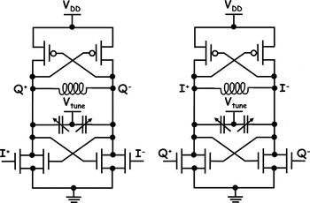
Figure 1 depicts the schematic of the designed QVCO. The circuit was biased without current mirror for sake of phase noise minimization [Reference Levantino, Samori, Bonfanti, Gierkink, Lacaita and Boccuzzi5]. In addition, the lack of a current mirror allows to reduce the power consumption [Reference Hajimiri and Lee6] and to avoid the introduction of a automatic amplitude control circuit [Reference Berny, Niknejad and Mayer7].
Schematic of the designed QVCO.

All the transistors were designed multi-finger and with a minimum channel length (0.13 µm). To get an equivalent admittance of the coupled pairs negative enough to compensate for the losses and robust enough against the fabrication tolerances, the p-channel transistors of coupled pairs were designed wider than the n-channel ones: the gate width of the p-channel transistors was fixed equal to 56 µm and the gate width of the n-channel transistors was fixed equal to 10 µm. For sake of good locking capability and of flicker noise minimization, the coupling n-channel transistors width was fixed equal to 16 µm.
The tank was designed using a single octagonal coil differential inductor resonating with the parasitic capacitances. A compact model as that described in [Reference Scuderi, Biondi, Ragonese and Palmisano8] was extracted from electromagnetic simulations carried out both with the 2D 1/2 electromagnetic simulator Momentum by Agilent Technologies and with the 3D electromagnetic simulator by CST. The inductor exhibits an inductance of about 290 pH and a maximum quality factor in the range of 27. It is worth pointing out that these values of inductance and quality factor are very close to those recently claimed in [Reference Dal Toso, Bevilacqua, Tiebout, Da Dalt, Gerosa and Neviani9] for a 65 nm CMOS LC VCO working in the Ku-band.
To obtain tuning capability, two 20-finger accumulation MOS varactors with a minimum gate length of 350 nm were introduced [Reference Tiebout10].
III. EXPERIMENTAL RESULTS
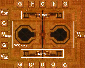
Figure 2 shows the microphotograph of the fabricated prototype. In the middle of the chip are visible the two inductors of the VCO core. In the microphotograph are also visible the two buffers to drive the load of the instruments. Under an experimental point of view, the use of the buffers is mandatory, in order to perform reliable measurements. Without buffers, the losses of the external load connected to the circuit during the characterization can degrade the VCO performance or, on the other hand, high-Q lines connected to the pads via the coplanar probes and coaxial cables can improve the VCO performance.
Microphotograph of the fabricated QVCO.

The GSGSG pads for the differential in-phase (I+, I−) and in quadrature (Q+, Q−) RF output signals are visible on the top and on the bottom of the chip, respectively. At the left side the pad GSG pad for the tuning voltage (V tune) is visible. Eventually, three pads for the supply (V DD) are distributed along the pad ring. The chip size is 900 × 1100 µm2, pads enclosed.
The differential output signals were made available to the single-ended input of the Agilent E4408B spectrum analyzer using a wideband Anaren 30070 hybrid.
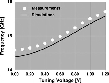
Figure 3 reports the output frequency variation with the tuning voltage. A difference less than 1.3% between simulations and measurements was obtained on the whole tuning range. The carrier frequency (f 0) goes from 14.6 to 15.8 GHz for V tune ranging between 0 and 1.2 V corresponding to a tuning range of 7.4%. The QVCO delivers about −20 dBm on a 50 Ω load and it sinks 9.4 mA from a 1.2 V supply.
Comparison between measured and simulated frequency dependence on the tuning voltage.

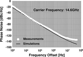
Phase noise measurements were carried out for V tune ranging between 0 V and 0.6 V using an Agilent E5500 phase noise meter. Figure 4 shows the measured phase noise for f 0 = 14.6 GHz. The QVCO exhibits a phase noise of −106 dBc/Hz at the offset frequency (Δf) of 1 MHz. This value is very close to the −107 dBc/Hz (at 1 MHz from a 10.7 GHz carrier) recently claimed for the VCO used in the PLL of a monolithic Ku-band receiver [Reference Myiashita2]. For other values of applied V tune the phase noise did not change in agreement with simulations.
Comparison between measured and simulated phase noise.

IV. DISCUSSION
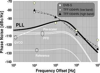
Since the VCO has to be employed in a PLL, the measured phase noise depicted in Fig. 4 has been therefore inserted in a PLL simulation carried out with Matlab. The noise contributions of the pre-scaler, of the phase and frequency detector, and of the reference have been set to typical values. The loop filter was designed so that to obtain a PLL bandwidth of 400 kHz and a phase margin of 60°. Figure 5 shows the simulated phase noise (black curve). The white lines are the contributions of the single building blocks.
Simulated PLL phase noise (black curve) together with the single contributions of the PLL building blocks (white lines) compared with the DVBS standard and the commercial product TFF1004HN.

The PLL phase noise is very close to the DVBS phase noise specifications (open circles) at the offset frequencies of 100 kHz and 1 MHz [11]. The simulated phase noise is a higher than standard limit in the offset frequency range 100 kHz–1 MHz. The simulated phase noise is also comparable with the phase noise exhibited by the TFF1004HN commercial product [4] and it is better for offset frequencies lower than 100 kHz. As further discussion about Fig. 5, it is worth pointing out that the phase noise and, in particular, the tuning range specifications have to be addressed by introducing a switched capacitor bank in the VCO topology during the design of the final PLL.
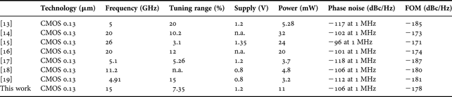
Eventually, the performance of the fabricated QVCO has been compared with other 130 nm CMOS VCOs reported in the literature through the following figure-of-merit (FOM) that allows for a comparison normalized with respect to the power and the frequency [Reference Fahs, Ali-Ahmad and Gamand12]:

where L(Δf) is the phase noise at Δf, and P DC is the dissipated DC power (Table 1).
Comparison with other 130 nm CMOS VCOs reported in the literature.
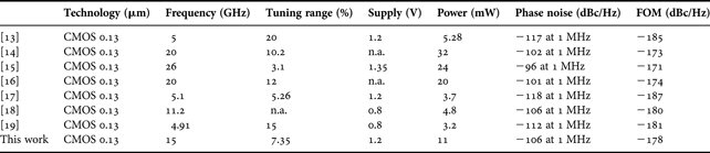
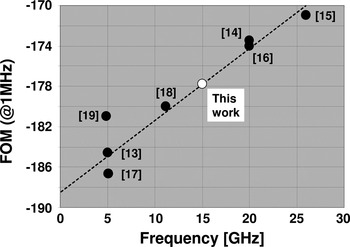
Figure 6 plots the FOM versus the oscillation frequency. The QVCO reported on the present work is well aligned with the other VCO's trend extracted from the literature.
FOM versus oscillation frequency. Comparison between the QVCO reported in the present work (white dot) and others VCOs reported in the literature (black dots). Technology is 130 nm CMOS in all cases.

A comparison with Ku-band cross-coupled VCO designed in 90 nm, see for instance [Reference Jacobsson, Bao, Aspemyr, Mercha and Carchon20], or 65 nm, see for instance [Reference Lu, Wang and Chang21], CMOS technologies does not point out a remarkable improvement in the phase noise even if these technologies are more expensive than the 130 nm CMOS adopted in the present work. The adoption of a 90 nm/65 nm CMOS technology may help with reducing the dissipated power and therefore with improving the FOM but not the phase noise in itself.
V. CONCLUSIONS
A 130 nm CMOS QVCO exhibiting a central frequency of 15 GHz has been demonstrated. The phase-noise-related FOM is well aligned with other 130 nm CMOS VCOs reported in the literature. In particular, the comparison with other CMOS VCOs claimed in the literature for Ku-band satellite receiver, with the DVB-S standard, and with commercial products implemented in SiGe BiCMOS technologies suggests that the 130 nm CMOS technology can be evaluated with interest for the design of a DVB-S satellite receiver front-end.
It is authors opinion that the main contribution of the present paper is not in the circuit topology in itself, that was already used in the past for a plant of applications, but rather in having provided demonstration that a bulk standard (e.g. not SOI) 130 nm CMOS technology can be employed to design a PLL for the realization of silicon monolithic DVBS satellite receivers, that nowadays were demonstrated only using bipolar or SiGe technologies.
In particular, the fact that the demonstrated VCO is an I/Q VCO allows for the conclusion that a DVBS receiver could be fabricated with a direct-conversion architecture implemented in a bulk 130 nm CMOS technology, which would be a product completely new with respect to a traditional superheterodyne one (e.g. a SiGe BiCMOS LNB cascaded with the low-voltage CMOS IF tuner).
Eventually, it has to be pointed out that in the final design of the PLL a QVCO topology exhibiting a switched capacitor bank will help with addressing the tuning range specifications.
ACKNOWLEDGEMENTS
The authors would like to thanks Andrea Mazzanti (University of Pavia, Italy) and Enrico Monaco (University of Modena and Reggio Emilia, Modena, Italy) for the fruitful discussions and Fahd Ben Abdeljelil (University of Nice, Nice, France) and the CIMPACA platform for the phase noise measurements.
The circuit was fabricated through the European CMP Consortium.
 Paolo Lucchi was born in Modena, Italy, in 1981. He received the Laurea degree in electrical engineering from the University of Modena and Reggio Emilia, Modena, Italy, in 2008. He is currently working toward the Ph.D. degree in electrical engineering at University of Modena and Reggio Emilia, Italy in co-tutele with University of Bordeaux, France. His research activity is focused on integrated circuit design for RF and millimeter-wave applications on CMOS technologies.
 Davide Dermit received the Laurea degree (summa cum Laude) in electrical engineering and the Ph.D. degree in Information and Communication Technologies from the University of Modena and Reggio Emilia, Modena, Italy, in 2007 and 2011, respectively, working on integrated circuit design for RF and mixed-signal applications on CMOS technologies. He is now with STMicrolectronics, Tours, France, working on the design of Si-based RFICs.
 Gilles Jacquemod received his Ph.D. degree in integrated electronics from INSA Lyon, in 1989. His primary research interests include analog integrated circuit design and behavioral modeling of mixed domain systems. He is also involved in RF design applied to wireless communication. He is head of electronics department of Polytech'Nice-Sophia, director of the CNFM PACA pole, and President of the CIM-PACA Design Platform. He is author or co-author of more than 100 journal and conference papers, and holds 2 patents.
 Jean-Baptiste Begueret received the M.S. degree in electronics in 1990 and the Ph.D. degree in 1996, both from the University of Bordeaux, France. In 1997, he joined IMS, the Microelectronics Laboratory of the University of Bordeaux, France, as an Associate Professor with the IC Design Team. From 2005 to 2010, he was leading this “IC Design Team”. In 2006, he became a full professor in this University. From 2011, he is the head of the “Design Group”. His research interests are in silicon ICs design for RF (up to 170 GHz) and high-speed data link (up to 100 Gbps) applications. He is currently a member of the IEEE BCTM and ICECS Steering Committee. He is also a member of the IEEE RFIT, RFIC, and ESSCIRC Technical Program Committee. He is co-author of more than 150 publications in international conferences, journals, and 20 patents.
 Mattia Borgarino received the Laurea degree in electronics engineering in 1993 and the Ph.D. degree in Information Technology from the University of Parma, Italy, in 1999. From 1999 to 2000, he was with the LAAS-CNRS, Toulouse, France, as Postdoctoral Fellow. In 2000, he joined the University of Modena and Reggio Emilia, Modena, Italy, where he is now Associate Professor. His current main research interests cover the design of Si-based RFICs.