Introduction
The constant growth of high-speed applications among satellite links is foreseen to foster the adoption of multi-band terminals. For instance, the pairing of Ku and Ka-bands will allow large spectrum for both uplink and downlink which in turn guarantees more high-quality services for the end users. If such services given by the High-Throughput Satellites and the Direct-to-Home internet access will be available everywhere without physical connections, their mass deployment will likely occur and the design of the mm-wave circuitry has to be compliant with large scale industrialization.
The electronic design of radio terminals is challenging: performance have to be maximized due to the low signal-to-noise ratio at the reception side while cost and compactness have to guarantee effective integration and affordable production. Since satellite communications usually rely on frequency division duplexing scheme, the diplexer (DPLX) plays a fundamental role in the architecture: its losses have a detrimental impact on the transmitted power as well as in the reception NF, while TX-RX isolation preserves the LNA from desensitization. The DPLX also acts as a physical connection between PCB and the waveguide/coaxial antenna port. The possibility to push such integration further is attractive to overcome the performance versus cost and complexity trade-offs.
The proposed design addresses the widely adopted Ku and Ka bands where the operation channels are 10.7–12.75 GHz (RX) and 27.5–30 GHz (TX). The approach described here exploits a low-pass and a high-pass filters (LPF + HPF) placed orthogonally. Since both integration and performance have to be maximized, a thin-film process has been chosen as manufacturing technique, which is well established and guarantees a straightforward path toward industrialization and large-scale production.
The choice of substrate integrated waveguide (SIW) approach leads to good quality factors especially above X-band, where the conductor losses tend to decrease [Reference Garg, Bahl and Bozzi1, Reference Bozzi, Georgiadis and Wu2]. The literature offers several examples of DPLX based on SIW solutions which fit the intended frequency bands: [Reference Sirci, Martínez, Vague and Boria3] shows a topology where two band-pass filters (BPFs) have been branched together but both placed within the X-band. The topology proposed in [Reference Jaschke, Rohrdantz, Mohncke and Jacob4] is similar to the previous one with the added complication of 10 GHz TX/RX frequency separation. The SIW approach has also been exploited for Ku-band tunable DPLX [Reference Iqbal, Tiang, Lee and Lee5], and X-band high isolation filters [Reference Cheng, Gu, Zhang, Yang and Huang6] to show the flexibility in the realization of different frequency behaviors.
Several published approaches also target compact footprint, especially across the lower part of the microwave spectrum. Li et al. [Reference Li, Mimsyad, Hou, Hsu and Ho7] and Dong and Itoh [Reference Dong and Itoh8] show DPLX structures for the S-band where the compactness is the main aim. The extreme shrinking leads to insertion loss (IL) penalty and degradation of the isolation between channels.
The proposed DPLX must exhibit an unusual wide frequency separation which will be mandatory to guarantee the aforementioned services. BPFs which exploit the fundamental mode of a standard rectangular cavity suffer from poor out-of-band rejection, limited by the first higher mode resonant frequency. SIW structures with wide out-of-band-rejection are available at the cost of higher IL and topology complexity.
As SIW circuits show intrinsic high-pass behavior, an integrated waveguide interconnection can be exploited as HPF across the 27.5–30 GHz span: it guarantees low in-band losses and high rejection across Ku band. SIWs unfortunately hardly suit the design of LPFs and for such reason the proposed DPLX embeds a nineth-order LPF based on open-ended microstrip stubs.
The novelty of this solution relies on the adoption of well-established concepts and their integration for maximum performance, compactness, and industrial fabrication. A planar DPLX on ceramic substrate covering such a wide portion of mm-wave spectrum is far from being standard and its design flow together with the achievable performance have been investigated and reported in this manuscript. This development is a significant part of the “Small user TErminal multi band DIplexer” (STEDI) project, which has been carried out thanks to the cooperation of two industrial partners and the European Space Agency. The manuscript is organized as follows: the section “Diplexer design and full-wave simulations” reports the design flow and the simulation results of the DPLX, the section “Realization and measurement” describes the manufacturing techniques and experimental results, and the section “Environmental analyses” comments on the reliability against thermal cycles and vibrations, and the final section concludes the paper.
Diplexer design and full-wave simulations
The intended DPLX is based on a single alumina substrate, only top and bottom metal layers are available for the circuit design and realization. The chosen topology for both filters has to be compliant with this straightforward approach and guarantees electromagnetic performance and compactness. Filter in-band IL is usually in trade-off with the achievable out-of-band rejection. The latter figure of merit is the first to be considered in order to design the DPLX's filters. The target rejections are 80 and 60 dB across RX and TX channels, respectively.
The final device is required to be as comparable as possible in terms of losses with a standard metallic waveguide filter, which is the conventional solution. The 99.6% 10 mils thick alumina with a dielectric constant (DK) of 9.85 and a dielectric loss tangent (DF at 1 MHz) of 0.0001 is selected to minimize the dimensions of the DPLX. The factors driving this choice are concentrated over dielectric constant stability and low dissipation factor. Furthermore, moisture absorption plays a relevant role in material's stability under certain environmental conditions, notably where high humidity is expected (outdoor applications). Alumina demonstrates multiple advantages compared with PTFE substrates nevertheless the good electrical properties. In example, moisture absorption is negligible for pure ceramic substrates but is relatively high (>0.02%) in most of Teflon-based dielectric laminates.
SIW-based high-pass filter
The intended TX band spans from 27.5 to 30 GHz. This path is designed as a symmetric straight SIW interconnection due to its intrinsic high pass behavior. Here the conventional paradigm of investigating very strong filtering functions to provide the required rejection (i.e. with a SIW line as long as possible), holds as long as the device is neither packaged nor shielded.
In the case at hand, in fact, the rejection across the RX band is limited by the cross-talk between the I/O ports of the component which may undesirably creep when the component is closed within a cavity. The choice of a SIW device is convenient because the top solid ground plane allows the placement of metallic septa between the ports: these decouple the HPF ports by suppressing surface waves and spurious couplings. By comparison, a conventional microstrip line would not accept such contacting metal structures on its top layer. These features guarantee high TX-on-RX isolation in a tiny footprint.
The width of the SIW (w SIW) defines the filter performance: the wider the opening the better the IL and the return loss (RL) across the TX band but the lower is the rejection on the RX channel. The dimensioning follows the standard rule by which the operating frequency of a rectangular waveguide is 1.25 times the cut-off frequency of the fundamental mode. Therefore, w SIW is given by

where c is the speed of light in vacuum, DK is the dielectric constant of the alumina (9.85), f TX1 is the lower frequency of the TX channel, d is the via diameter and s is the center-to-center distance between vias. Assuming d = 250 μm and s = 1.9⋅d, w SIW becomes 2300 μm (the layout is shown in Fig. 1).
2D layout of the DPLX. Orange shapes show the top metal layer of the layout, blue circles the metallized vias, the green area is the package footprint.

The equivalent rectangular waveguide width is 2173 μm, and its propagation constant at 12.75 GHz can be computed to be 10.2 dB/mm. As a consequence, the expected length to provide at least 80 dB of isolation is about 8 mm, provided that spurious coupling between ports is made negligible.
The 50 Ω microstrip to SIW transition and the length of the filter have been optimized through Ansys Electronics Desktop. The considered target S-parameters are the in-band RL (|S11| <−20 dB) and the RX rejection (|S21| <−80 dB).
Microstrip low-pass filter
Within the Ku-band, microstrip lines still show a reasonable Q-factor which allows a low-loss 50 Ω matched filter design. In particular, the designed LPF exploits the convenient topology of open-ended stubs connected through a high-impedance line.
Although being very practical for integration, microstrip lines suffer from radiation, which can be lowered by reducing substrate thickness. Clearly, this feature is in trade-off with the conductor losses which become large with thinner substrates.
In order to achieve the desired RX-on-TX rejection, the filter order has been chosen equal to nine. The synthesis response guarantees up to 70 dB of the attenuation in the TX band but, due to the inter-port cross-talk, this value seems unreachable when implemented in a compact planar and packaged component. A reasonable expectation for simulations of a packaged component without any metal septum to isolate the ports is 60 dB while considering at the same time an IL below 0.6 dB. Figure 1 shows the final layout.
Diplexer full-wave simulations
As mentioned within the introduction, the approach proposed here relies on the mixing of well-established and reliable concepts to deliver a high-performance and compact mm-wave DPLX. Beside the single filter design, the relative placement of the HPF and LPF filters plays a fundamental role in the final DPLX features.
The frequency span from 10.7 to 30 GHz needs a wideband tee which can be achieved only by means of a TEM or a quasi-TEM structure (i.e. microstrip). Options on multimode cavity [Reference Kordiboroujeni and Bornemann9] or ultra-wide band SIW structures [Reference Moscato, Moro, Pasian, Bozzi and Perregrini10] have been explored but they are not compatible with the given specifications.
The filters have been chosen to match an orthogonal topology, like the one adopted in [Reference Teberio F, Arregui, Soto, Laso, Boria and Guglielmi11]. This choice, shown in Fig. 1, allows compactness, isolation, and short branching, which mitigates the risk of spurious resonances between the channels. This kind of topology requires a large empty area between the two orthogonal paths. This area has been exploited to ground the top metallized layer and has also been used as footprint for metallic septa. Both strategies enhance the isolation between TX and RX ports. The final device features a 15 × 11.1 mm2 compact footprint which is one of the key aspects in the whole project.
The exploited thin-film manufacturing technique allows the use of an SMD-compliant process, therefore a proper wide-band and low-loss transition has been designed. The one chosen to connect the DPLX to a carrier PCB is based on a metallized half-via. This choice is reliable, assures good performance and guarantees visual inspections after the soldering process.
The design of such transition matches two 50 Ω lines realized on different layers and through different technologies. Layer-to-layer transitions suffer at high frequency where the series inductance of the metallized via starts to be problematic. In order to compensate such effect, a corona close enough to the signal pad and extra matching elements as shown in Fig. 2 have been designed. The required signal-to-ground gap involved is the bottleneck because the standard tolerance given by the PCB process and by the soldering procedure. This trade-off between operational frequency and reliability has been overcome with the proposed design.
Layout of the PCB-to-alumina transition. Dimensions are in μm: D1 = 250, D2 = 300, L1 = 430, W1 = 880, W2 = 400. The figure also shows the PCB and alumina stack up.

A metallic package 5 mm height milled from aluminum has been also realized. It helps the shielding of the component while the inner metallic septa maximize the TX rejection. Both antenna and RX ports (which rely on unshielded structures) are in the same package cavity, therefore their rejection could be limited by cross-talk between transitions. The enclosure design foresees three apertures to avoid short circuits between the 50 Ω microstrip and the ground on the top layer of the alumina substrate. Each aperture has a width of 2 mm and a height 0.75 mm, large enough to avoid performance drop due to small misalignments.
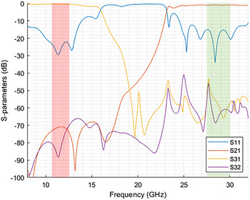
The stand-alone DPLX has been simulated and optimized without any metal packaging. The achieved EM performances are promising and totally fulfill the given specifications. Furthermore, the assembly (PCB + DPLX + package) has been modeled and simulated within the Ansys environment. The results are shown in Fig. 3 and reported in Table 1. The achieved isolation performance oversteps the intended specifications due to spurious effects given by the metallic package, the PCB, and the connectors.
Simulated frequency behavior of the developed DPLX. Carrier PCB, package, and connectors shape have been considered. Red highlighted frequency span shows the RX channel while the green rectangle shows to the TX one.

Simulation versus measurement comparison.

Realization and measurement
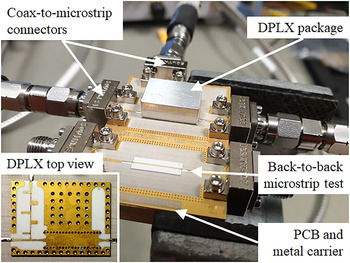
The DPLX has been realized within SIAE Microelettronica facilities, as the whole thin-film SMD compliant process can be internally handled. The process exploits a 10 mils-thick AD996 alumina from Coorstek Inc. and a Ti-Pd sputtered layer with a galvanic gold finishing. The SMD compatibility is guaranteed by a nickel shield while a final flash of gold preserves the whole metal stack-up. A carrier PCB has also been designed on a 10 mils Teflon laminate (Arlon CLTE-AT). The package has been realized in-house, manually aligned and bonded on the DPLX with conductive glue. A curing procedure is finally required. The whole assembly is shown in Fig. 4.
Final assembly of the DPLX under measurement and die top view.

The experimental setup involves the use of a 4-port Rohde&Schwarz ZVA40 VNA, where coaxial cables are connected to the carrier PCB through 2.92 mm female Southwest end-launch transitions, finally fastened on a brass carrier. A custom 3-port TRL calibration has been applied to all the measures in order to de-embed the mismatches and the losses given by the coaxial-to-microstrip transitions.
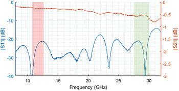
The characterization also concerns the measurement of a 50 Ω microstrip 10.25 mm long realized on the same alumina substrate and soldered on the PCB (Fig. 4). This is useful to prove the effectiveness of the losses and matching achievable by using the half-via transition. Figure 5 shows the measurements of such back-to-back microstrip soldered on the test PCB.
Characterization of the back-to-back microstrip soldered on the test PCB. Red highlighted frequency span shows the RX channel while the green rectangle shows to the TX one.

The verified |S11| touches its worst value of −17.7 dB at 22 GHz. For the other frequencies, the graph instead shows matching better than 20 dB up to the top of the TX band nevertheless. The measured IL is below 0.7 dB across the sub-10−30 GHz frequency span. It is important to highlight that within the measured |S21| of the DPLX, the pair of the half-via transition contributes by a relevant percentage.
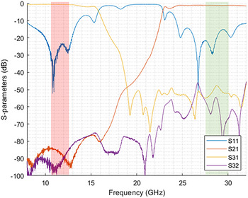
Figure 6 shows the S-matrix of the assembled DPLX measured using the three-port setup. The agreement between simulations and measurements confirms the accuracy of the design procedure. The detailed performance is reported in Table 1.
Measured S-parameters of the realized DPLX. Absorber has been placed on the top of the package to lower cross-talk between ports. Red highlighted frequency span shows the RX channel while the green rectangle shows to the TX one.

Preliminary measurements show a TX-on-RX rejection value in the order of 50 dB. The reason of this value was mostly related to the crosstalk between the ports when all the parts were assembled together. The measured |S21| shown in Fig. 6, where such isolation is better than 80 dB, is the correct one achieved with an absorber placed on the top of the component. On the contrary, the RX-on-TX rejection (|S31| in Fig. 6) is still limited by the package and PCB assembly. The design of the carrier PCB also plays a role: the design does not take into account shielding vias. and ground planes along the feeding microstrips which could potentially help to reduce crosstalk between the ports. Finally, the matching from all three ports, as well as the IL across both TX and RX path are in line with the expectations.
Environmental analyses
The intended application of the developed component is related to equipment for satellite ground-segment where the environmental conditions are limited by terrestrial standards, much less demanding than their space counterparts. However, the developed component covers an unusual wide frequency span and furthermore it is soldered on a PCB. Such features could lead to large performance deviation due to environmental stresses. As a consequence, both thermal characterization and mechanical tests have been carried out to investigate the DPLX stability under harsh ambient conditions.
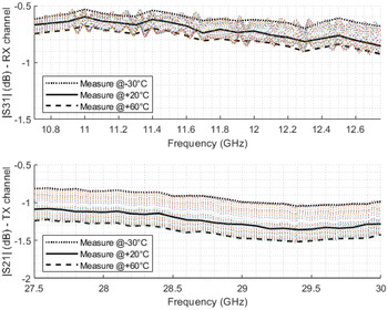
The DPLX has been initially tested in a thermal chamber from −30°C to +60°C with a temperature slope of 0.5°C/min. Three hundred measurements have been automatically acquired. Their superposition is shown in Fig. 7. The frequency shift due to the temperature variation is not taken into account due to large FBW of the filters. The main results concern the variation of the |S21| and |S31| parameters in their passbands against temperature whereas both RL and isolation between channels do not show any relevant spread. The RX features an in-band IL deviation from 0.45 to 0.95 dB which is in line with the expectations. On the contrary, the TX channel shows a deviation which is 0.3 dB larger, from 0.71 to 1.56 dB. This spread is under investigation but the three-times-higher operating frequency and nickel's temperature coefficient of resistance (0.0059°C−1, which is twice the gold one) are deemed the main culprits.
Detail of transmission parameters and superposition of acquisitions during thermal test. Top graph shows the RX channel; bottom graph shows the TX channel.

The environmental testing of the designed DPLX includes also a mechanical vibration setup articulated in two procedures: sine vibration and random vibration. The purpose of the first test is to determine any mechanical weakness or degradation in the specified performance. On the other hand, the purpose of the random vibration test is to understand how the DUT withstands over its life cycle, where all the environmental mechanical stresses are summed together.
Pre- and post-vibrational tests measurements of the alumina diplexer show negligible variations in the S-matrix which in turn means high robustness against a wide spectrum of mechanical stress. The performance stability over thermal and vibrational stress is in-line with the expectations which delivers a higher TRL of the proposed component.
Conclusion
A novel hybrid topology DPLX for Ku/Ka-bands has been presented. The use of a microstrip LPF and an SIW-based HPF has been demonstrated, which is also compatible with the unusual frequency separation between channels and wideband operation. A suitable design of shielding package has been also described to improve isolation between ports. The thin-film technology allows compactness, easy integration at PCB level, and thermal/mechanical stability, which has been proven by experimental electrical and environmental tests. The technology readiness level of the developed component is suitable for future low-cost, small and low-weight ground-segment multi-band equipment.
Acknowledgements
This work was supported by the ESA under project number 4000123762/18/NL/CLP (ARTES AT).
 Stefano Moscato was born in Pavia, Italy in 1988. He received the M.Sc. and Ph.D. degrees in electronics engineering from the University of Pavia, Italy, in 2012 and 2016, respectively. He was a visiting Ph.D. student at Georgia Tech, Atlanta, GA, USA, in early 2015. From May 2017, he became part of the R&D microwave group of SIAE Microelettronica S.p.A, Milano, Italy. His research activities have been focused on RF-to-mm-wave passive components and antennas. He is now involved in the design of waveguide and planar devices for E-band point-to-point radio links. Dr. Moscato was a recipient of an IEEE MTTS Undergraduate/Pre-Graduate Scholarship in 2012. He has been the Chair of the IEEE Student Branch, University of Pavia, from 2013 to 2016.
 Giandomenico Cannone was born in Bari, Italy, in 1984. He received the M.Sc in Telecommunications Engineering at the Politecnico di Milano, Italy, in July 2009 with a thesis on the design of microwave diplexers for satellite applications with Universidad Politecnica de Madrid (ETSIT). Since 2010, he works as senior RF and microwave engineer at SIAE Microelettronica S.p.A and his activity is related to the development of RF-to-mm-wave diplexers, power dividers, orthomode transducers, isolators/circulators and antennae measurement. Since 2020, he works also as project manager on ESA ARTES AT activities related to the design and development of mm-wave high power amplifiers.
 Matteo Oldoni was born in Milan, Italy, in 1984. He received the B.Sc. degree in telecommunications engineering and M.Sc. degree from the Politecnico di Milano, Milan, Italy, in 2006 and 2009, respectively, and is currently working toward the Ph.D. degree at the Politecnico di Milano. His master's thesis concerned the synthesis of microwave lossy filters. He is currently involved in the field of microwave filters. His research interests include synthesis and design techniques for microwave filters, algorithms development for computed-aided tuning, and improvement of numerical methods applied to electromagnetics. Mr. Oldoni was the recipient of the Young Engineers Prize of the 39th European Microwave Conference, Rome, Italy, 2009. He is currently with SIAE Microelettronica S.p.A.
 Davide Tiradossi was born in Perugia, Italy, in 1992. In 2016–2017 he carried out his master thesis and internship in Ericsson (Goteborg) on the design of MW matching transition at D-band under the advice of Prof. Sorrentino. He received his master degree (with merit) in electronic and telecommunication engineering from University of Perugia in April 2017. Since May 2017 he is working at RF Microtech as RF and microwave R&D engineer in the microwave filter and passive components area.
 Luca Pelliccia received his Ph.D. degree on electronics engineering at University of Perugia with a thesis titled “Tunable and miniaturized waveguide filters for advanced communication systems” under the advice of Prof. Roberto Sorrentino. He is currently working at RF Microtech Srl (where he is an associate member) as Head of the microwave filter and passive components division. His research and design activities include innovative concepts for compact, tunable and high-performance filters and diplexers. His research involvement has resulted in the publication of several papers in the proceedings of international microwave conferences and journals.
 Petar Jankovic was born in Donji Milanovac, Serbia in 1976. He received engineering diploma from University of Belgrade in 2000. After studies, he joined Institute of Microwave Techniques and Electronics in Belgrade until 2006 when he moved to Spain and joined Acorde Technologies, a spin-off company from the Faculty of Telecommunication in Santander. He worked as design engineer at Acorde Technologies at RF product department dealing with the development and manufacturing of high technology subsystems and components for the Satellite Telecommunications and Defense Sector until 2017. Since 2017, he joined European Space Agency as a microwave engineer in RF technology and Equipment section.
 Fabrizio De Paolis received the Laurea degree in electronic engineering and the Ph.D. in applied electromagnetics from “La Sapienza” University of Rome, Italy. In 2005, he joined COM DEV International, Cambridge, ON, Canada, as an advanced member of technical staff. He was involved in the modeling and design of high-frequency devices for space applications. He was also the technical lead of commercial satellite programs for worldwide prime contractors. Since 2009, he has been with the European Space Agency across various sites, where he was initially responsible for industrial and R&D contracts related to RF equipment and technologies. His current activities encompass the areas of ground segment RF and antennas for next generation satellite communication systems.