Introduction
The current communication scenario around the world is primarily remote-based. Thus, there is a great deal of reliance on wireless communication devices. As a result, demands for broadband and high data rate systems have also been increased. Besides, the IoT has gained interest in different fields, starting with home automation, smart cities, healthcare, etc. Hence the challenge for the research community is to appease these demands. The ultra-wideband (UWB) frequency spectrum (3.1–10.6 GHz) has the potential to mitigate such demands. Currently, the researchers are working on the UWB antenna, which is an essential part of wireless communication systems. However, there is a problem of interference with the existing narrowband applications such as WiMAX (3.2–3.8 GHz) and WLAN (5.1–5.8 GHz). An UWB antenna with low radiation efficiency for these bands is very desirable.
UWB antenna design involves a better understanding of the various system parameters such as gain, fractional bandwidth, radiation characteristics, etc. A detailed knowledge of UWB electromagnetics, components, and system engineering has been well documented in [Reference Zwick, Wiesbeck, Timmermann and Adamiuk1] by dividing into various topics which are very beneficial for the research community. Researchers have proposed both planner and non-planner type of antenna structures [Reference Fereidoony, Chamaani and Mirtaheri2–Reference Sun, Cheung and Yuk4] to attain operational bandwidth over entire UWB spectrum with good radiation characteristics. The planner type hexagonal radiator may provide higher average peak gain and better efficiency as compared to other regular planner structure [Reference Sun, Cheung and Yuk4]. Many articles have been published on the subject of attaining band-notch properties. Some of those have reported single-band elimination [Reference Peng and Ruan5–Reference Peng, Wang, Zhao and Liu11] characteristics. However, the single notched band would not be sufficient to implement the design for practical applications. So, UWB antennas with dual band-notched properties have also been investigated and designed [Reference Chu and Yang12–Reference Mayuri, Rani, Subrahmanyam and Madhav, Boddapati23]. To attain a single notched band effect, mushroom type EBG structure [Reference Peng and Ruan5], grounded stub [Reference Weng, Cheung and Yuk6], and C-shaped stub [Reference Bhattacharya, Roy, Chowdhury and Bhattacharjee7] beside the feedline have been realized. U-shaped slot on the patch [Reference Mandal and Das8, Reference Shi, Cui, Liu, Lv and Sun9], sorting pin-loaded structure [Reference Wong, Huang, Mao, Chen and Chu10], and SRR loaded on the ground plane [Reference Peng, Wang, Zhao and Liu11] have also been considered by the researchers to obtain a single notch effect. Furthermore, for achieving dual notched bands, etching of slots having different shapes on the radiating element has been adopted by the researchers. C-shaped slots [Reference Chu and Yang12, Reference Indu and Kanaujia13], U-shaped slots [Reference Mandal and Das14, Reference Singh, Khanna and Singh15], combinations of C-shaped and U-shaped slots [Reference Chaabane, Djahli and Redadaa16], SRR and SIR type slots [Reference Li, Li and Ye17], and L-shaped slots [Reference Mighani and Akbari18] have been presented in some literature. Different types of slots on the radiating patch create interference on the surface current, and as a result, the antenna becomes non-responsive at this frequency. In the article [Reference Srivastava and Mohan19], combinations of slots both in radiating patch and ground plane are used for notching effects in two different bands. In the article [Reference Hoseyni, Nourinia, Ghobadi, Masumina and Mohammadi20], a circular-shaped split-ring parasitic element in the ground plane along with a rectangular split-ring slot on the patch has been used to obtain a band notch for the WiMAX band. The effects of L-shaped stubs loaded UWB antenna with a slot on the feed line have been demonstrated [Reference Guichi, Challal and Denidni21]. Iron-shaped and inverted U-shaped parasitic resonators in the ground are being used to achieve dual notch properties for a circular UWB antenna [Reference Yadav, Abegaonkar, Koul, Tiwari and Bhatnagar22]. Reconfigurable UWB antenna using pin diode has also been proposed to realize notch characteristics [Reference Mayuri, Rani, Subrahmanyam and Madhav, Boddapati23]. An overview of different kinds of proposed work on UWB antenna has been well discussed in [Reference Adamiuk, Zwick and Wiesbeck24]. It has been observed from some articles that the excitation of the radiating patch has been provided by microstrip line feed or CPW line feed technique with different shapes of radiator such as circular, rectangular, triangular, and hexagonal. Few structures have been modified to realize desired impedance bandwidth.
In this paper, an UWB antenna with dual-band rejection characteristics has been proposed. The radiating element is hexagonal and poses a wide impedance bandwidth of 10 GHz (2.4–12.4 GHz), i.e., 135% of the center frequency. A meandered S-shaped slot has been etched out on the patch, and a notched band from 3.2 to 3.8 GHz has been achieved experimentally, which will be useful to eliminate the WiMAX band. Furthermore, a notched band from 5 to 6 GHz is achieved experimentally after incorporation of an inverted U-shaped slot on the ground plane placed below the feed line. Hence it can successfully eliminate the WLAN band. The proposed design of the hexagonal microstrip antenna has been fabricated and measured. The radiation characteristics and reflection parameter of the proposed design have been measured using a vector network analyzer. An acceptable similarity has been observed between the simulated and measured data. A vector network analyzer has been used to measure the parameters of the fabricated antenna, and a good agreement between the simulated and measured results has been observed.
Antenna design and structure
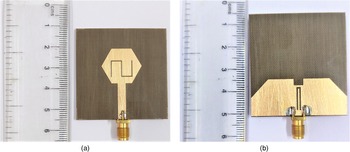
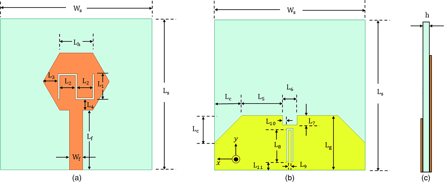
The reference and proposed antenna structures are shown in Figs 1 and 2, respectively. The values of the designing parameters in mm have been depicted in Table 1. It has been designed using electromagnetic solver Ansys HFSS. Arlon AD300A has been chosen as a substrate with dielectric constant ɛ r = 3, thickness h = 1.524 mm, and loss tangent 0.002. The radiating element of the proposed design is hexagonal. Initially, the antenna has been designed without any slots or defects on the ground plane and the radiating element. The fabricated structure of the proposed antenna is shown in Fig. 3. The design has been optimized through simulation in multiple stages. The variation of the reflection coefficient (S 11) with frequency for different stages of design has been shown in Fig. 4. At stage 1, a simple hexagonal antenna with a partial ground plane has been simulated. Next, on stage 2, a rectangular slot has been etched out in the ground plane below the microstrip line along with corner chamfering. At stage 3, a meandered S-shaped slot on the radiating patch has been utilized. Finally, at stage 4, an inverted U-shaped slot in the ground plane under the feedline has been engraved. The structural modification on different stages is depicted in Fig. 5.
Structure of the reference antenna.

Structure of the proposed antenna, (a) radiating plane, (b) ground plane, and (c) side view.
Fabricated structure of the proposed antenna, (a) radiating patch and (b) ground plane.

Simulated reflection coefficient (dB) in different stages of the design.

Structural modification in different stages of the design.

Design parameters of the proposed antenna (units are in mm)

In stage 1, the antenna poses a relative impedance bandwidth of 3 GHz over which S 11 ≤ −10 dB. The impedance bandwidth has been improved to 11 GHz (S 11 ≤ −10 dB) by implementing the modification on the ground plane at stage 2. The antenna covers the frequency spectrum (2.54–12.25 GHz), in which the entire UWB has also been covered. With the addition of a meandered S-shaped slot in the radiating element, a notched band from 3.14 to 3.82 GHz has been obtained, which is depicted in stage 3. It is possible to eliminate the WiMAX (3.2–3.8 GHz) band due to this implementation. Lastly, at stage 4, the inverted U-shaped slot on the ground plane has produced a notched band from 5.1 to 5.85 GHz, which eliminates the WLAN band (5.2–5.8 GHz) is also possible.
Parametric study
Several parametric studies concerning different designing parameters have been carried out to determine the optimum values of the same such that we would obtain the desired results. The study of the proposed design has been performed using the EM simulator Ansys HFSS. The characterization of the antenna is outlined as follows.
Effect of the variation on slot length L1
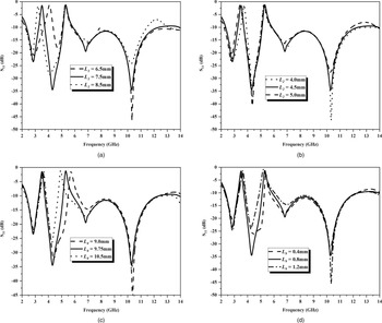
The slot length along the y-direction for the meandered S-shaped slot on the radiating patch is depicted as L 1. The deviations in the value of L 1 are responsible for shifting the center frequency of the lower notch band. The lower notch band has been obtained for eliminating the WiMAX band. The value of L 1 has been varied between 6.5 and 8.5 mm, and the accepted value is 7.5 mm as per the parametric study shown in Fig. 6(a). Hence, the increment of the value of L 1 shows the shifting of the frequency to the lower side. The value of L 1 is optimized for 7.5 mm to have the desired notched band from 3.2 to 3.81 GHz.
Simulated return loss (dB) plots with variation of the (a) slot length L 1 of the S-shaped slot, (b) slot length L 2 of the S-shaped slot, (c) slot length L 8 of the U-shaped slot, (d) slot length L 9 of the U-shaped slot.

Effect of the variation on slot length L2
The slot length along the x-axis of the meandered slot on the radiating element has been denoted as L 2. Though the very nominal variation in the lower notch band has been observed, the value of L 2 has been taken as 4.5 mm to achieve the desired result. The parametric study regarding the variation of the S-parameter with the variation of L 2 has been shown in Fig. 6(b). The value of L 2 has been varied between 4 and 5 mm.
Effect of the variation on slot length L8
The length of the inverted U-shaped slot toward the negative y-axis is marked out as L 8, as shown in Fig. 2(b). Due to the variation of L 8, the second notch-band center frequency is varying, keeping other resonant frequencies unaffected. The higher notch band is responsible for eliminating the WLAN band. The value of L 8 has been varied from 9 to 10.5 mm, for which the notch-band center frequency has been varied from 4.8 to 5.5 GHz. It has been observed from the study shown in Fig. 6(c) that the notched band has been shifted lower side with the increasing length of L 8. To achieve the desired response, i.e., the elimination band for 5.1–5.85 GHz, the length of L 8 has been fixed to 9.75 mm.
Effect of the variation on slot length L9
The slot length along the x-axis of the inverted U-shaped slot is marked as L 9, as depicted in Fig. 2(b). Due to the deviation of the value of L 9, there is a noticeable change in the bandwidth of the second notched band. With the increasing value of L 9, the width of the elimination band has also been increased, which is depicted in Fig. 6(d). So, the optimum value of L 9 has been taken as 0.8 mm to eliminate the 5.1–5.85 GHz band, which has been allocated for WLAN.
Results and discussion
The return loss characteristics and the radiation parameters of the fabricated antenna have been measured using the vector network analyzer and standard microwave test bench setup. Both measured and simulated results are showing good harmony between them. The minimal deviation between the measured and simulated results may be due to the simulation error, loss of cables and connectors during the measurements, and tolerance in manufacturing. The measured and simulated reflection coefficients of the proposed antenna are shown in Fig. 7 and Table 2.
Variation of reflection coefficient with frequency of the proposed antenna.

Simulated and measured results of the proposed antenna

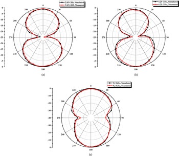
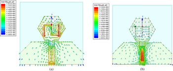
The fabricated antenna with the slots on the radiating patch and the ground exhibits dual notch bands of 3.2–3.8 and 5–6 GHz as per the measured results. The simulated and measured gain of the proposed antenna has been shown in Fig. 8. The simulated and measured radiation patterns of E-plane co-polarization at 2.85, 4.25, and 9.2 GHz, respectively, have been shown in Figs 9(a)–9(c). In order to witness the significance of the slots in getting the band notches, the simulated vector current distribution in the radiating patch and the ground plane of the proposed antenna at the center frequencies, 3.48 and 5.48 GHz of two notched bands, has been shown in Figs 10(a) and 10(b).
Variation of the gain with frequency of the proposed antenna.

Normalized E-plane co-polarization radiation pattern of the proposed antenna for (a) 2.85 GHz, (b) 4.25 GHz, (c) 9.2 GHz.

Simulated current distribution of the proposed design at (a) 3.48 GHz, (b) 5.48 GHz.

In the proposed design, the meandered slot on the patch has been utilized to obtain the notch band in the frequency range 3.2–3.8 GHz (WiMAX) and the inverted U-shaped slot has been introduced to achieve the notch band in the frequency range 5–6 GHz (WLAN). The total length of the slots has been calculated approximately as half guided wavelength at the center notch frequency. From the simulated current distribution of the designed antenna shown in Fig. 10, the center notch frequency for both the slots may be predicted by the equation [Reference Shi, Cui, Liu, Lv and Sun9],

where c is the speed of light in free space, ɛ r is the dielectric constant of the substrate, and L s is the total calculated slot length.
The total slot length of the meandered slot has been calculated as L s1 = 31.5 mm, shown in Fig. 11(a), and for which the center notch frequency has been approximated as 3.37 GHz, and the total slot length of the inverted U-shaped slot has been found as L s2 = 20.3 mm, shown in Fig. 11(b), using which the approximated second notch center frequency has been calculated as 5.22 GHz. Slot length dimensions have been exhibited in Fig. 2, and values have been given in Table 1. The predicted notch frequencies from equation (1) have been found very close compared to both the simulated and measured results which have been depicted in Table 3.
Current path length for the elimination band centered at (a) 3.48 GHz and (b) 5.48 GHz.

Center frequencies of the elimination bands for proposed antenna

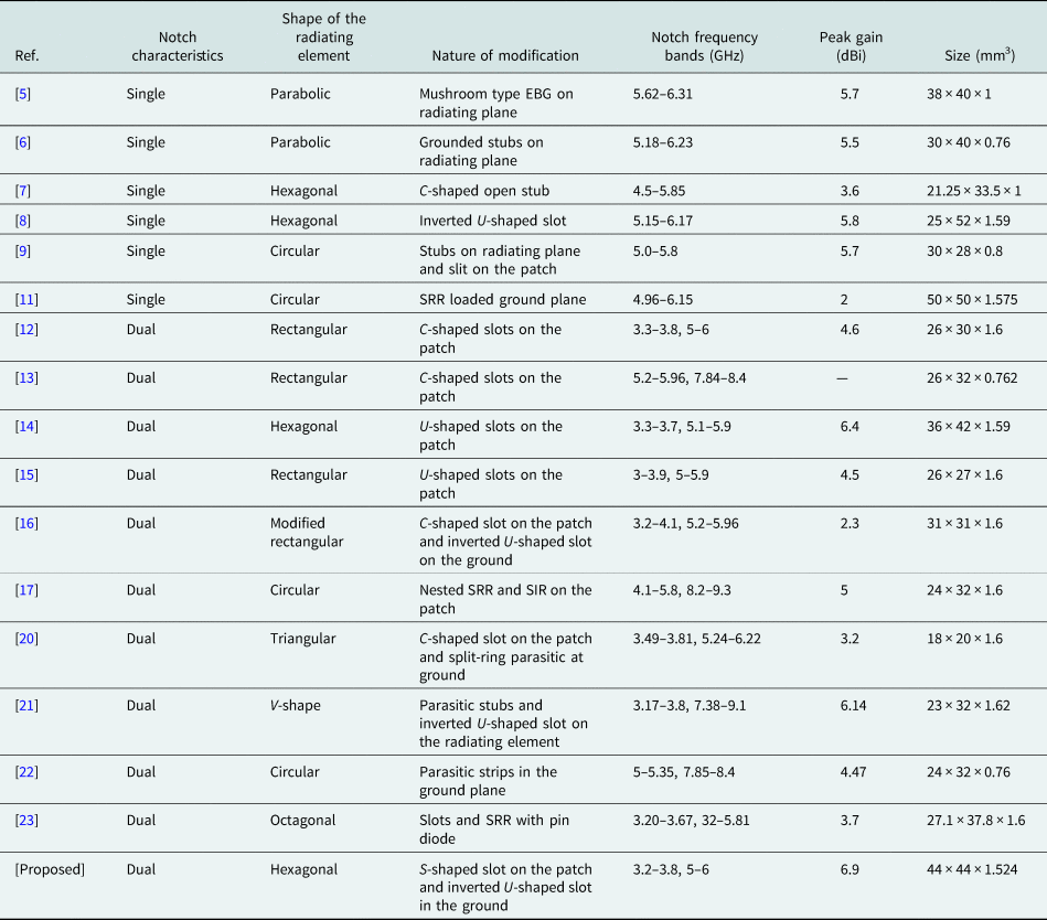
The comparison studies have been obtained and presented in Table 4. From the given comparison studies, it has been observed that the proposed antenna in this literature has been found as the best suitable one for wireless communication systems with perfect elimination bands for WiMAX and WLAN applications.
Comparison study of proposed antenna with the cited literature
Conclusion
In this literature, a hexagonal UWB microstrip patch antenna with dual band-notched characteristics has been designed and practically implemented. The proposed design can be useful to eradicate interference issues between the UWB system to the widely used narrowband systems such as WiMAX and WLAN. The design layout has been simulated using full-wave EM simulator Ansys HFSS and experimentally validated. The proposed antenna has attained an impedance bandwidth of 10 GHz (2.4–12.4 GHz), i.e., 135% of center frequency for VSWR ≤ 2. The realized gain and radiation patterns have also been figured out and found quite admissible for the entire UWB range 3.1–10.6 GHz. The effects of slots on the radiating element and the ground plane have been investigated through several parametric studies presented in this paper. Optimum dimensions have been noted to realize desired elimination bands for 3.2–3.8 GHz (WiMAX) and 5–6 GHz (WLAN) bands.
Acknowledgement
The authors acknowledge the Department of Electronics and Communication Engineering, Central Institute of Technology, Kokrajhar, India, for providing support and assistance to perform the measurements of the fabricated prototype of the proposed antenna. Special thanks to Manoj Sarma for his help and support to carry out the measurement process.
Conflict of interest
None.
 Surajit Mukherjee was born in Hooghly, West Bengal, India in 1985. He received his B.Tech. degree in electronics and communication engineering from Maulana Abul Kalam Azad University of Technology (formerly known as West Bengal University of Technology), West Bengal, India, in 2007, and M.Tech. degree in electronics and communication engineering (microwaves) from the University of Burdwan in 2009. Currently, he is pursing Ph.D. degree in electronics and communication engineering from the Central Institute of Technology, Kokrajhar, Assam, India. He is currently working as an Assistant Professor in Haldia Institute of Technology, West Bengal, India. His research interest includes multiband and ultra-wideband antennas.
 Avisankar Roy received his B.Tech. and M.Tech. degrees in electronics and communication engineering from Maulana Abul Kalam Azad University of Technology (formerly known as West Bengal University of Technology), WB, India, in 2006 and 2009 respectively. He has his obtained Ph.D. in engineering from the University of Kalyani, Kalyani, WB, India in 2018. His area of research interest includes microstrip antenna design and frequency-selective surfaces. He has contributed to numerous research articles in various journals and conferences of repute. He is currently working as an Associate Professor in the Department of Electronics and Communication Engineering, Haldia Institute of Technology, Haldia, WB, India.
 Smarajit Maity has obtained his B.E. in electronics and instrumentation engineering from Vidyasagar University in 2002. He earned his M.E. degree in electronics and telecommunication engineering from Bengal Engineering College (presently known as Bengal Engineering and Science University/Indian Institute of Engineering Science and Technology, Shibpur) in 2005. He is currently working as an Assistant Professor in the Department of Electronics and Instrumentation Engineering, Academy of Technology, Adisaptagram, West Bengal. He has published three research articles in reputed journals and conferences. His area of research interest includes microstrip antenna, frequency-selective surface, optoelectronics devices, photovoltaic system, etc.
 Tapas Tewary has obtained his B.Tech. in electronics and communication engineering from Kalyani Govt. Engineering College, Kalyani University, India in 2004. He earned his M.Tech. degree in VLSI design from the Institute of Radiophysics and Electronics, Calcutta University in 2008. He is currently working as an Assistant Professor in the Department of Electronics and Communication Engineering, Academy of Technology, Adisaptagram, West Bengal. He has published five research articles in reputed conferences. His area of research interest includes microstrip antenna, frequency-selective surface, VLSI design, optoelectronics devices, etc.
 Partha Pratim Sarkar was felicitated with a Ph.D. in engineering from Jadavpur University in 2002. He has obtained his M.E. from Jadavpur University in 1994. He earned his B.E. degree in electronics and telecommunication engineering from Bengal Engineering College (presently known as Bengal Engineering and Science University/Indian Institute of Engineering Science and Technology, Shibpur) in 1991. He was in the rank of Reader during the period January 1997 to January 2005. He is presently working in the rank of Professor since January 2005 at the Department of Engineering and Technological Studies, University of Kalyani. His area of research includes microstrip antenna, microstrip filter, frequency-selective surfaces, and artificial neural network. He has contributed around 310 research articles in various journals and conferences of repute. He has supervised 16 Ph.D. students, 47 M.Tech. thesis and more than 70 B.Tech. projects. He is also a Life Fellow of IETE and IE (India).
 Sunandan Bhunia has obtained his B.Tech. and M.Tech. from the Institute of Radiophysics and Electronics, Calcutta University in 2002 and 2004, respectively. He has obtained Ph.D. degree in engineering from Jadavpur University in 2009. He was awarded gold medal from Vidyasagar University for first class in physics (H) in 1999. He is currently working as an Associate professor in the Department of Electronics and Communication Engineering, Central Institute of Technology, BTAD, Assam. He has published about 50 research articles in reputed international and national journals and conferences. His area of research interest includes microstrip antenna, microstrip filter, and frequency-selective surfaces, VLSI, etc.