I. INTRODUCTION
In the last two decades, concerns about rising energy demands have resulted in a concentrated search for cost-effective alternative renewable sources of energy. Organic photovoltaics (OPVs) based on conjugated polymers and fullerene derivatives have gained considerable interest, as they seem to be potentially well suited to address the above-mentioned needs.Reference Burroughes, Bradley, Brown, Marks, Mackay, Friend, Burns and Holmes1–Reference Roth, Blumentritt, Burghard, Cammi, Carroll, Curran, Dusberg, Liu, Muster, Philipp and Rabenau3 There has been over the last decade a misnomer that OPVs would not require some of the clean room conditions required by their thin film counterparts. However, this is not the case, and equal care in cleanliness and a number of different deposition steps are required. Nevertheless, in simple quantity of materials, OPVs have significant advantages, which include less physical semiconductor materials required for a similar photonic response in generating excitons, devices produced require fewer industrial steps, and of course, one of the biggest benefits is that they are lightweight and can be deposited in many ways.Reference Liao, Yambem, Haldar, Alley and Curran4 The processability of organic semiconductors at room temperatures allows us to use simple deposition techniques such as spin-coating, doctor-blading, or ink-jet printing.
Ink-jet printing as a solution-dispensing tool has many attractive features due to its precise and versatile deposition technique.Reference Kawase, Shimoda, Newsome, Sirringhaus and Friend5–Reference Singh, Haverinen, Dhagat and Jabbour7 Its noncontact deposition technique makes it substrate and application independent allowing printing on flexible and nonflat substrates of different sizes. It allows the dimensional controlled deposition of inks on targeted locations up to micron-scale accuracy. The two-dimensional (2D) patterning ability negates the need of masks and thus, an extra fabrication step. This tight control also helps in keeping the wastage of materials to a minimum. As such, the technique is favorably disposed toward integration in industrial scale production, providing cost reduction of existing components as well as provides opportunities for pioneering new strategies. In addition, high mechanical flexibility has been a major advantage of OPVs since it enables processing using flexible substrates.Reference Haldar, Yambem, Liao, Alley, Dillon, Barron and Curran8, Reference Yambem, Liao and Curran9 Novel architectures focusing on orienting the OPV vertically to maximize the photon trapping and enhancing performance have been reported by our group.Reference Curran, Talla, Dias and Dewald10–Reference Alley, Dias, Liao and Curran12 The photoactive layer(s) of the vertically oriented OPV needs to be deposited around its circumference. To exploit the complete benefit of such structures, more than one wrap of the photoactive layer is needed, which requires a deposition of long homogeneous strip(s) of accurate dimensions only attainable by ink-jet printing.
The performance of bulk heterojunctions (BHJ) OPVs is very sensitive to the active layer morphology, which determines charge dissociation as well as charge transport. It becomes imperative to consider how the processing conditions affect the morphology of the printed photoactive layer and the performance of the OPVs. Currently, the knowledge as to how this morphology is affected by various printing parameters is incomplete. There have been studies of using high boiling point solvents as a part of the solvent mixture or using additives to improve the performance of OPVs.Reference Hoth, Choulis, Schilinsky and Brabec13–Reference Eom, Senthilarasu, Uthirakumar, Yoon, Lim, Lee, Lim, Lee and Lee15 Aernouts et al.Reference Aernouts, Aleksandrov, Girotto, Genoe and Poortmans14 printed a poly(3-hexylthiophene):phenyl-C61-butyric acid methyl ester (P3HT:PCBM) blend dissolved in a chlorobenzene (CB) and a high boiling point solvent, tetrahydronapthalene. Hoth et al.Reference Hoth, Choulis, Schilinsky and Brabec13 fabricated an ink-jet-printed cell using an ortho-dichlorobenzene (oDCB):mesitylene mixture at a substrate temperature of 40 °C. Power conversion efficiency (PCE) of 3.7% using a high boiling point additive, 1,8-octanedithiol, at a substrate temperature of 25 °C has been demonstrated by Eom et al.Reference Eom, Senthilarasu, Uthirakumar, Yoon, Lim, Lee, Lim, Lee and Lee15 Lee et al.Reference Lee, Lee, Kim, Lee and Kang16 reported that the best OPV performance was observed from ink-jet printing condition of around 50% of droplet overlaps with 2 wt% P3HT:PCBM blend in CB at a substrate temperature of 25 °C. These reports suggest that by changing various parameters, more than one optimum set of parameters for the fabrication of OPVs can be obtained. However, there is a deficit in understanding of the role of these parameters, which of them are necessary or more important than others. Gaining a deeper understanding of these parameters will allow us to efficiently optimize the processing conditions required to achieve the maximum performance. In this study, we tested the effects of different printing pattern for the fabrication of OPVs. We present a comparison study of three printing methods [multiarray (MA), single layer array, and multilayer array] where parameters, such as concentration of the solution and drop spacing, were varied. We also investigated the influence of various annealing parameters on their electrical and optical properties and correlated them with the device performance.
II. EXPERIMENTAL DETAILS
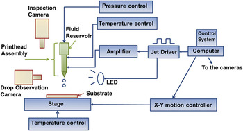
Ink-jet printing of the organic photoactive layer was carried out using a Jetlab 4 tabletop printer (MicroFab Tech, Inc., Plano, TX). The ink-jet printer consists of a piezoelectric-driven ink-jet head with X–Y motorized stage, which has a heating element, and a drop observation camera used to observe the formation and the pathways of the ink droplets. The schematic diagram of the printer is shown in Fig. 1. The drop ejection process starts when the fluid-filled reservoir of the printhead is subjected to an applied external voltage pulse, causing it to contract and reduce in volume. This volumetric change causes a sudden compression of the fluid creating an acoustic shock wave, and this overcomes the surface tension at the ink–air interface and causes the ejection of the drop from the printhead tip orifice. These types of systems are referred to as drop-on-demand since the voltage is applied only when a drop is desired. The computer is used to program and set the parameters of the waveform, the print pattern, and control the motion of the stage.
Schematic diagram of the printer.

The active materials, regioregular poly(3-hexylthiophene-2,5-diyl) (P3HT) (MW ∼87,000, head-to-tail regioregularity ∼98%) and [6,6]-phenyl-C61-butyric acid methyl ester (PC61BM) (>99% purity), were obtained from Sigma-Aldrich (St. Louis, MO). The host solvents, CB, oDCB, and mesitylene, were also purchased from Sigma-Aldrich. Poly(3,4-ethylenedioxythiophene):poly(styrenesulfonate) (PEDOT:PSS) (Clevios PH 1000, Heraeus Clevios GmbH, Leverkusen, Germany) was used as hole transport layer. All chemicals were used as received without any further purification.
The OPVs used in this study have the structure: Indium Tin Oxide (ITO)/PEDOT:PSS/active layer/Al, where the active layer is a P3HT:PCBM blend with a weight ratio of 1 to 0.68. The ITO coated glass substrates (8–12 Ω/□ surface resistivity; Aldrich, St. Louis, MO) were etched using aqueous 18% HCl solution and zinc powder to pattern the electrode. The substrates were cleaned by successive ultrasonic treatment in 1.75% micro-90 solution, water, and isopropyl alcohol baths for 15 min each. The cleaned substrates were treated with ozone plasma for 10 min to improve the wettability of aqueous PEDOT:PSS onto the ITO substrate. The PEDOT:PSS layer was spin-coated at 3000 rpm for 2 min to form a thin hole transport layer on the ITO substrate. After baking at 80 °C for 1 h, the active layer was printed on top of the PEDOT:PSS layer. A bipolar waveform with voltages of 13–18 V and dwell times of 34–40 μs was used to print the P3HT:PCBM inks. For each concentration of the P3HT:PCBM solution, the voltage was optimized for stable jetting. Films were printed at different velocities from 5 to 50 mm/s. The increase in the print velocity decreased the film uniformity, and therefore, all the print patterns were printed at 5 mm/s. Subsequently, the some samples were transferred into a jar filled with CB vapor for 30 min, at room temperature or at 60 °C, to allow solvent annealing. Solvent annealing of the films at temperatures higher than 60 °C degraded the film homogeneity and created visible pinholes. Finally, the top metal cathode of Al was thermally evaporated on top of the photoactive layer through a custom made shadow mask under vacuum with a pressure of 8 × 10⁻⁴ Pa. The active cell area, which is defined by the overlap area of anode and cathode, was around 1 mm2 for all the devices. All devices were encapsulated before measurement. Thermal annealing of the devices was carried out at 150 °C for 5 min by keeping the OPVs in contact with a hot plate inside the glove box.
A Keithley 2400 SourceMeter unit (Keithley Instruments, Inc., Cleveland, OH) was used to perform the current–voltage (I–V) measurements using an Abet LS 150 Xenon Arc Lamp Source (Abet Technologies, Inc., Milford, CT) coupled with an AM 1.5 filter at room temperature without correction for spectral mismatch. For accurate measurements, the light source was precisely calibrated using a standard silicon solar cell (Oriel 91150V Solar Reference Si Cell) certified by the National Renewable Energy Laboratory. To ensure the accuracy of the reported values, two sets of measurement of standard ITO/PEDOT:PSS/spin-coated P3HT:PCBM/Al were carried out: one with an aperture mask having the same areas of the cells and one without. The I–V characteristic ratios for short-circuit current density (J SC), open-circuit voltage (V OC), fill factor (FF), and PCE of these two sets of devices (eight cells for each) were used to calculate the final performance of the ink-jet-printed cells, which were all carried out without an aperture mask.
The optical absorption of the P3HT:PCBM blend films printed on PEDOT:PSS coated glass slides were measured using an OCEAN OPTICS spectrometer (model HR2000+, Ocean Optics, Inc., Dunedin, FL). The UV–Vis absorption data of the P3HT:PCBM films are obtained after the subtraction of the absorption of the PEDOT:PSS covered substrates from the total absorption measured. The surface profile was characterized by a Tencor AlphaStep 200 surface profilometer (KLA-Tencor Corporation, Milpitas, CA).
III. RESULTS AND DISCUSSION
A. Methods of printing of P3HT:PCBM ink: MA, multilayer single array, and single layer single array
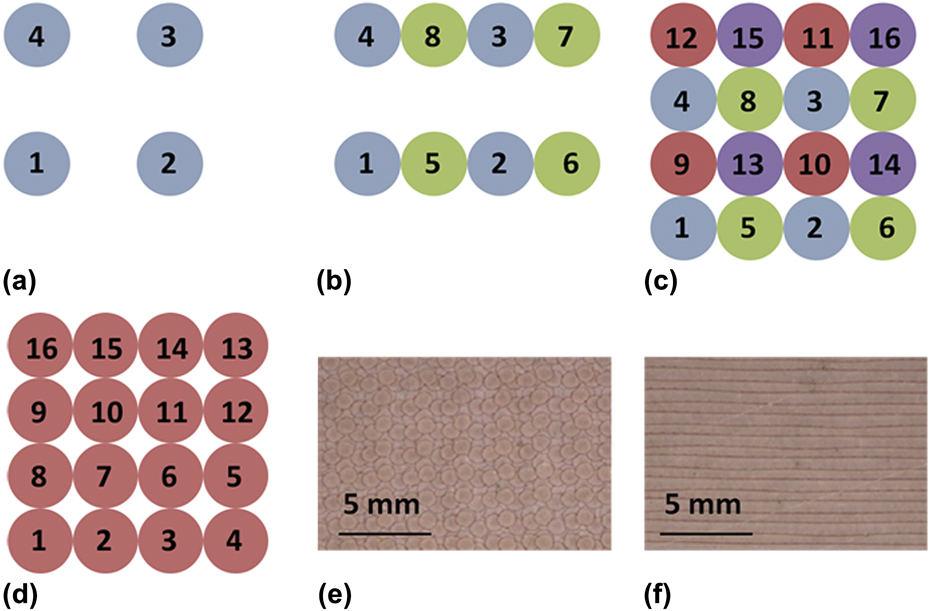
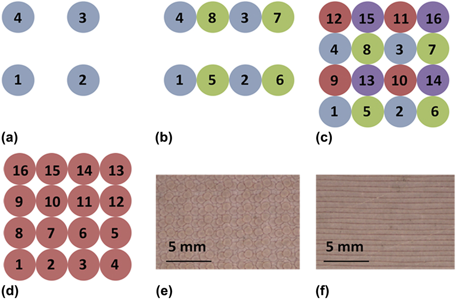
The most commonly used printing patterns are lines or arrays [Fig. 2(d)]. In the drop-on-demand mode of the ink-jet printer, a drop can be dispensed at a predefined point on the substrate. The adjacent drops merge together and form a continuous film when the drop spacing is decreased to a threshold value. The degree of overlap between adjacent lines can be varied to get different patterns. In this study, four matrices were printed with their degree of overlap being controlled by the spacing between their origins. This pattern is a variation of the array pattern and has been referred to as the MA pattern [Figs. 2(a)–2(c)]. A detailed study on the fabrication of defined and homogeneous films by ink-jet printing has been reported by Tekin et al.Reference Tekin, de Gans and Schubert17 The partial drying of the first array before deposition of the second was beneficial in creating homogeneous films. It was concluded that the MA pattern rather than single array (SA) pattern resulted in regular and smooth films. In this study, however, we discovered that the MA pattern was not suitable for printing the active layer of OPVs.
Schematic representation of the MA (a–c) and SA (d) pattern with no overlap. The numbers represent the sequence in which the drops are dispensed. The dots of the same color belong to the same matrix and are deposited at the same run. All the patterns are printed in bidirectional mode. To form a MA pattern, (a) the first matrix is printed, (b) the second matrix is printed as defined by spacing between the origins of the matrices, and (c) the final pattern after the printing of the third and fourth matrices. (d) The SA pattern with no overlap. Images of (e) MA and (f) SA print pattern.
Apart from depending on the print pattern, uniform film formation also depends on solvent formulation.Reference Shimoda, Morii, Seki and Kiguchi18 The spreading of the ink on the substrate is affected by the surface tension of the solvent, while the drying behavior is determined by their evaporation. A high boiling point solvent is used to prevent the precipitation of the solute and the clogging of the printhead, resulting in more effective long-term output. However, a low boiling point solvent increases the evaporation rate, thus avoiding the coffee ring formation and leading to the formation of a film with better morphology. In this paper, we report the study of the BHJ OPVs fabricated with ink-jet-printed P3HT:PCBM layer with various printing methods. To ensure the accuracy of the reported values, two sets of measurement of eight standard ITO/PEDOT:PSS/spin-coated P3HT:PCBM/Al devices were carried out: one set with an aperture mask and one without. The conversion ratios were calculated to be 0.85, 0.98, 1.05, and 0.88 for J SC, V OC, FF, and PCE, respectively. These ratios were used to determine the final performance parameters of the ink-jet-printed cells, which were characterized without an aperture mask. The detailed device performances are summarized in Table I.
Power conversion efficiencies of the BHJ OPVs fabricated with ink-jet-printed P3HT:PCBM layer with various printing patterns: MA, single layer SA, and their respective concentrations. The values are averaged over 8–10 devices.

In our first study, a mixture of oDCB and mesitylene was used as the solvent to form the ink.Reference Hoth, Choulis, Schilinsky and Brabec13 The concentration was kept low at 1.25 g/L. The optimum absorbance of the active layer of 0.3–0.4 optical density (OD) (based on the parameters of optimized spin-coated OPVs) was obtained by using multiple passes of the printer. Although various print patterns and substrate temperatures were used, it was difficult to maintain the consistency of the pattern formation and films printed with identical parameters varied visually with average efficiencies of the resulting OPVs less than 0.01%.
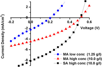
On the contrary, printing of MA pattern using a 1.25 g/L solution of P3HT:PCBM in CB with multiple passes led to more reproducible results. The resulting printed layer showed great homogeneity visually. The OPVs exhibited relatively better performance although with low J SC (1.78 mA/cm2) and V OC (0.18 V) (Fig. 3). The device characteristics remained poor with a typical efficiency of 0.095%. This poor performance may be due to the incomplete merging of the drops. This hypothesis gains more credibility when we consider that in ink-jet printing, the films are created by depositing discrete drops on top of each other and neighboring drops intermix to create a continuous film. Incomplete mixing of drops may potentially result in regions of isolated domains. The shunt resistance calculated was only 124 Ωcm2 and the series resistance was 64 Ωcm2. This resulted in a significant loss of photo-generated current. Printing a MA pattern with a higher concentration of 10 g/L showed an improved performance with an efficiency of 0.59% (V OC = 0.45 V, J SC = 3.30 mA/cm2, FF = 0.34). The shunt resistance increased to 205 Ωcm2 and the series resistance decreased to 51 Ωcm2.
Current–voltage curves for the BHJ OPVs fabricated with ink-jet-printed P3HT:PCBM layer with three different printing conditions under AM 1.5 illumination (100 mW/cm2): MA with low concentration (circles), MA with high concentration (triangles), and SA with high concentration (squares).

The improved device performance was attributed to the reduced number of arrays and hence, reduced number of drops used to achieve the required absorbance. As a result of this finding, it followed that the best performance should be obtained by the limiting case of the MA pattern, which is the single layer SA pattern. Devices were fabricated using single layer SA pattern with concentration of 10 g/L P3HT:PCBM solution. The device performance showed a significant increase with the efficiency at 1.29% (Fig. 3). The J SC showed a 91% increase from 3.30 to 6.29 mA/cm2. The V OC and FF were 0.50 V and 0.41, respectively. The shunt resistance was 157 Ωcm2 and the series resistance further decreased to 18 Ωcm2.
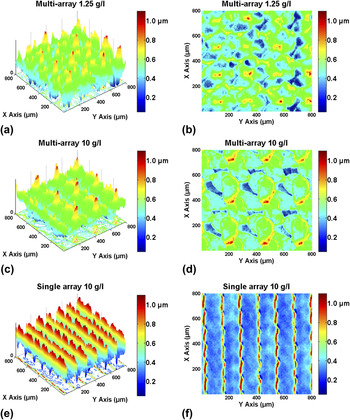
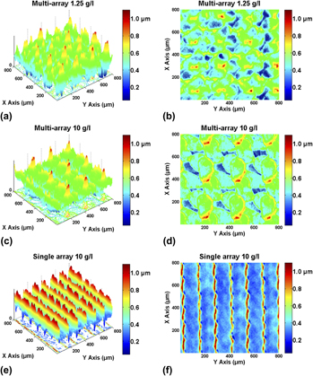
Profilometry studies of the films revealed a remarkable morphology. The images are representative of the surface morphology on top of a base layer of the blend (Fig. 4). The drops did not merge uniformly with its neighboring drops; instead, each drop left a dense deposit along the perimeter to form a coffee ring pattern as it dried.Reference Deegan19 The solute accumulated at the outer perimeter and created a ridge-like structure along the circumference. When another overlapping drop was deposited, it partially dissolved the previous drop but also created its own coffee ring pattern. The entire MA film when seen under an optical microscope showed a pattern of intersecting coffee rings. The average height of the ridge for the case of MA film was ∼700 nm.
Images corresponding to surface morphology of the three different printing conditions: (a and b) MA with low concentration, (c and d) MA with high concentration, and (e and f) SA with high concentration. The images are representations of the film surface obtained using an optical microscope and converted to three dimensional using a Matlab program. The color scale gives the height profile of the film. The 2D images in the right-hand column indicate the height variation of the film topology.

The entire device can be approximated as thin film OPVs connected in parallel with thick film ones. Thick film OPVs are associated with poor performance due to low carrier mobility and space charge effects.Reference Lenes, Koster, Mihailetchi and Blom20, Reference Moule, Bonekamp and Meerholz21 Even though the absorption is enhanced by increasing the thickness of the photoactive layer, it also leads to the buildup of space charge, which decreases the electric field and thus, the dissociation efficiency.Reference Lenes, Koster, Mihailetchi and Blom20 Also, the charge recombination losses are high due to the increased distance traversed by the carriers to reach their respective electrodes. Consequently, the J SC is very low for thick film OPVs because of leakage current and charge recombination. Furthermore, the reduced exciton efficiency is also responsible for the inferior V OC in thick film devices.Reference Koster, Mihailetchi, Ramaker and Blom22 These thick film OPVs in parallel with the thin film OPVs do not contribute significantly to any photocurrent and instead reduce the V OC of the total device. Additionally, it has been reported that as the film thickness increases, the series resistance increases and shunt resistance decreases.Reference Kim, Kim and Kim23 These thick regions will probably adversely affect their neighboring OPVs by providing shunt pathways for their charges and thus, reducing the overall device performance. The low shunt resistances of the devices can be attributed to the presence of the ridges. The region covered by the ridges for 1.25 g/L MA pattern is estimated to be 56% and 53% along the X- and Y-axis, respectively. The percentage reduced for the 10 g/L MA pattern to 46% (X-axis) and 41% (Y-axis). The number of drops used to create the film was higher for the low concentration MA pattern and this coincided with an increase in the amount of film area lost due to the formation of thick regions along the drop perimeters. The improved device performance of the high concentration MA OPVs can thus be attributed to the reduced number of drops required to create the film. Profilometry studies of devices fabricated using SA pattern with concentration of 10 g/L P3HT:PCBM solution showed a striated topography [Figs. 4(e) and 4(f)]. The ridges were present but they were uniformly distributed along the X- and Y-axis. The area lost reduced to 0% along the X-axis and was 41% along the Y-axis. A correlation between the area lost due to the formation of thick film ridges and the decrease in the performance of the OPV was observed. The percentage of thin and useful region was highest in SA pattern, and thus, it gave the best performance as expected.
Using SA print pattern, OPVs with efficiency of one order of the magnitude higher than that printed with MA with the same absorption were obtained. In addition, more reproducible results were seen for the case of SA print pattern with the standard deviation of only 9%. In contrast, the standard deviation for the devices fabricated by the MA print pattern reaches as high as 30%. Therefore, it can be concluded that single layer SA print pattern provides a 2-fold advantage, i.e., it gives the highest efficiency as well as the most consistent performance. This result proves the significance of printing in a single layer SA pattern for the performance of BHJ OPV devices.
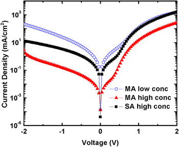
To further investigate the effect of different patterns, dark current density–voltage log-linear curves were plotted for the BHJ OPVs fabricated with ink-jet-printed P3HT:PCBM layer with three different printing conditions (Fig. 5). Negative bias is defined as negative voltage applied to the ITO contact and positive voltage on Al. The current in forward bias was much larger compared to the reverse bias current. The rectification ratio for the cells with MA low concentration blend of 1.25 g/L was only 7.13 at ±2 V. At a reverse bias voltage of −2 V, MA low concentration cell gave a current density of 211 mA/cm2. Such a large reverse current density for MA low concentration cell is an indication of the large number of leakage paths, which can form due to incomplete integration of the drops. Increasing the blend concentration for MA decreased the reverse current density and the rectification ratio increased to 96.25 at ±2 V. The SA cells printed with 10 g/L showed the highest rectification ratio of 123.89 at ±2 V. This further demonstrates the advantage of films formed using a single layer SA pattern for OPV fabrication. A set of OPVs were also fabricated with a low concentration in a multilayer SA pattern. Due to the low concentration of the blend, 16 complete passes were required to obtain an absorbance of 0.41 OD. The profilometry studies show that even though the area lost was 0% along the X-axis but was high at 78% along the Y-axis. This can be correlated to the large number of passes used for the fabrication of the film. The surface morphology resembled ridges with very narrow “valleys.” These “valleys” are the regions that have the required thickness to effectively dissociate excitons. A decrease of these “valleys” led to a decrease of device performance. The corresponding average device efficiency was 0.02% with low J SC of 0.42 mA/cm2.
Semilogarithmic representation of dark current density–voltage curves for the BHJ OPVs fabricated with ink-jet-printed P3HT:PCBM layer with three different printing conditions: MA with low concentration 1.25 g/L (circles), MA with high concentration 10 g/L (triangles), and SA with high concentration 10 g/L (squares).

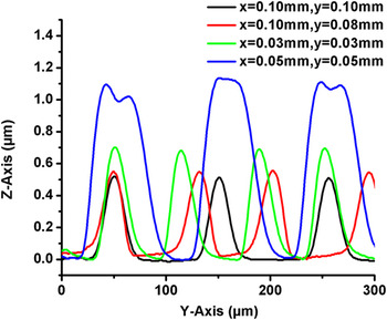
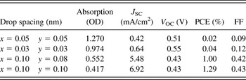
The single layer SA pattern was also printed using 20 g/L P3HT:PCBM solution (Table II) with different drop spacings to study how the overlaps affect OPV efficiencies. The drop spacings were adjusted to get the required absorbance. When the drop spacing was less than 0.1 mm, the efficiency was in the range of 0.02–0.05%. When the drop spacing was 0.1 mm (0% overlap), the device performance showed a significant increase with the efficiency at 1.29%. However, the film homogeneity was lost on further increasing the drop spacing to more than 0.1 mm, which the film is comprised of individual lines. Profilometry studies show the different profiles along the Y-axis (Fig. 6). As the overlap increases, the region covered by the ridges increases: from 47% for 0% overlap to 85% for 50% overlap along the Y-axis, which corresponds to a decrease in the performance. This proves that increase in the thick ridge regions will lead to poorer performances, irrespective of the pattern. This also proves the universality of the single layer SA pattern. Similar OPV efficiencies can be achieved as long as the absorption is controlled to be ∼0.4 OD and the area covered by ridges is less than 50%.
Cross sections obtained by profilometry of the ink-jet-printed P3HT:PCBM films in the Y-direction using the SA print pattern. The cross sections correspond to varying overlaps (details in the inset).

Device parameters of the BHJ OPVs fabricated with ink-jet-printed active layer with different film absorption. The films were printed with SA print pattern with a P3HT:PCBM blend of 20 g/L concentration in CB. The values are averaged over 5–8 devices.

B. Annealing conditions of printed single layer array OPVs: Solvent annealing, thermal annealing, and other combinations
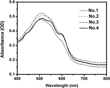
The morphological changes due to various annealing treatments on the active layer of the OPVs are reflected by the changes in their optical properties. For a given thickness of film, the maximum optical absorption is a direct function of its crystallinity.Reference Kim, Liu, Namboothiry and Carroll24Figure 7 shows the effect of annealing on UV–Vis absorption spectra for the films of P3HT:PCBM printed on PEDOT:PSS coated glass slides. The untreated P3HT:PCBM film (No. 1) displayed a broad absorption peaks centered at 500 and 550 nm and one shoulder at 600 nm. These three bands can be attributed to the intrinsic π–π* transitions of P3HT.Reference Brown, Thomas, Köhler, Wilson, Kim, Ramsdale, Sirringhaus and Friend25, Reference Shrotriya, Ouyang, Tseng, Li and Yang26 After the films were thermal annealed (No. 3), the spectrum showed increased absorption across the spectrum and a redshift of peak absorption wave length (λmax) by 5 nm without any significant change in the shape of the shoulders at 550 and 600 nm. Solvent annealing carried out at room temperature (No. 2) caused the λmax to redshift by 14 nm. Its absorption, though higher than the untreated film, was less than that of the thermal annealed films. After solvent annealing at 60 °C (No. 4), the UV–Vis spectra showed an increased absorption compared to the untreated case and a redshift of 12 nm.
UV–Vis absorption spectra obtained for P3HT:PCBM thin films with different treatments: unannealed (No. 1), solvent annealed at room temperature (No. 2), thermal annealed (No. 3), and solvent annealed at 60 °C (No. 4).

Since all the films were fabricated under similar conditions, the change in the peak absorption wave length after annealing can be attributed to an increased interchain interaction among P3HT chains. The increased interchain interaction among the P3HT chains results in a lower energy state of more delocalized conjugated π electrons and causes the lowering of the band gap between π and π* resulting in the observed redshift in the peak absorption wave length.Reference Shrotriya, Ouyang, Tseng, Li and Yang26 The absorption spectrum peaks were higher for the thermal annealed case than any other annealing condition. However, the most prominent effect of solvent annealing treatment at 60 °C was that the three vibronic peaks were much more pronounced than the ones observed in both the thermal annealed and the solvent annealed films, indicating a higher degree of ordering.Reference Sundberg, Inganäs, Stafström, Gustafsson and Sjögren27, Reference Li, Shrotriya, Huang, Yao, Moriarty, Emery and Yang28 The pronounced peaks of film No. 4 suggest that solvent annealing at 60 °C causes a greater degree of ordering, due to the self-organization of molecules through the convection medium of the solvent with the aid of extra thermal energy provided. The solvent molecules at higher temperature have an enhanced molecular mobility and it will facilitate the movement of the molecules during the process of self-organization.Reference Ryu, Cha and Jang29 The surface of the films fabricated by the SA pattern show a striated topography. Thermal annealing and solvent annealing at room temperature does not change the topography. In comparison, a 30% reduction in peak height has been observed when solvent annealed at 60 °C. The reduction in the height of the ridges indicates some recovery of previously “dead” regions by decreasing the percentage of regions covered by these ridges. A decrease in the region covered by the ridges leads to improved device performance.
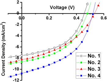
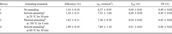
Figure 8 shows the J–V characteristics under illumination for the printed OPVs before and after various annealing treatments. The device performance was significantly affected by the annealing conditions as shown. The unannealed OPVs showed an average PCE of 1.43% (V OC = 0.45 V, J SC = 6.27 mA/cm2, FF = 0.49). The series resistance was 14.48 Ωcm2 and the shunt resistance was 239.23 Ωcm2. After thermal annealing the OPVs, the V OC increased significantly to 0.54 V and an improvement of J sc (7.26 mA/cm2). The average shunt resistance of the devices decreased to 197.47 Ωcm2 and this led to a reduction in FF from 0.49 to 0.42. The increase in V OC and J SC compensated for the decrease in FF and led to an improvement in PCE from 1.43% to 1.63%. Solvent annealing at room temperature caused the PCE to increase to 1.54% with the V OC unchanged (0.45 V). The series resistance declined slightly to 13.11 Ωcm2 and the shunt resistance also decreased to 163.18 Ωcm2, correspondingly the FF reduced to 0.45. The J SC showed a minor increase (7.51 mA/cm2). After solvent annealing at 60 °C, the OPV exhibited the lowest series resistance at 10.09 Ωcm2 and the maximum shunt resistance at 240.43 Ωcm2. The devices exhibited the best PCE of 1.99% with the highest value of J SC (7.89 mA/cm2), the V OC was 0.51 V, and the FF was 0.49. The increase in J SC originates from the increased degree of P3HT domain crystallinity as indicated by the UV–Vis absorption curves. The summary of device performance of various OPVs fabricated in this study is provided in Table III. The solvent annealed OPVs where subsequently thermal annealed as well. The average device performance degraded from 1.54% to 0.99% for the devices solvent annealed at room temperature and from 1.99% to 1.54% for the devices solvent annealed at 60 °C. This suggests that the crystalline domain size have already reached their optimum limit after solvent annealing for 30 min, and further annealing leads to excessive coarsening of the domains, which increases exciton recombination and hinders efficient charge transport. This is analogous to the degradation of OPV performance on thermal annealing at high temperatures.Reference Wang, Pearson, Lidzey and Jones30
J–V curves of OPVs under AM 1.5 illumination (100 mW/cm2): unannealed (No. 1), solvent annealed at room temperature (No. 2), thermal annealed and after (No. 3), and solvent annealed at 60 °C (No. 4).

Characteristic parameters of the BHJ OPVs fabricated with ink-jet-printed P3HT:PCBM layer with various annealing treatments under AM 1.5 illumination (100 mW/cm2). All the values are averaged over 16 devices.

a Before Al deposition.
b After Al deposition.
IV. CONCLUSIONS
We fabricated ink-jet-printed OPVs using P3HT:PCBM in CB and investigated the effect of print pattern and annealing treatment on the efficiency of the OPVs. When MA or multilayer SA pattern was used to fabricate the active layer, the device performance was poor with efficiency less than 1%. A single layer SA print pattern was more suited for the fabrication of OPVs. The OPVs fabricated with the single layer SA films gave an average efficiency of 1.29% as well as the most consistent performance. The optimum annealing condition for the printed OPV was determined to be solvent annealing at 60 °C, giving an efficiency of 1.99% for the single layer SA devices. Solvent annealing at higher temperatures yields films with greater degree of crystallinity by allowing the P3HT films to self-organize over a longer period of time as opposed to conventional thermal annealing. Even though morphological studies have been done on spin-coated or doctor-bladed OPVs, the results of those studies cannot be directly transferred to the ink-jet films, which present unique challenges. The results obtained in this paper represent important steps toward the better understanding of the ink-jet printing process of polymers for OPVs.
ACKNOWLEDGMENT
This work is supported by the Office of Naval Research, Department of Defense under Grant No. DD-N000141110069.