200 °C), while a-IZO metallized with Mo remains amorphous. The effects of the unstable Ti/IZO interface are shown to include: vacancy injection, enhanced amorphous-to-crystal transformation kinetics, interfacial oxide formation, and the lateral growth on adjacent IZO of rutile TiO
I. INTRODUCTION
Rapid progress has been made in recent years in the development of amorphous oxide semiconductor (AOS) materials for thin-film transistor (TFT) applications. One of the most promising of the AOS materials systems is based on indium oxide with Zn added to stabilize the amorphous phaseReference Yaglioglu, Yeom and Paine1 and ternary cation additions of Ga,Reference Hosono2 Hf,Reference Chong, Jo and Lee3 and SiReference Chong, Kim and Lee4 to suppress carrier generation. These materials appear likely to be integrated into the TFTs used as pixel switching elements in the next generation of active-matrix liquid crystal display, active-matrix organic light emitting diode , and foldable electronic paper (e-paper) display technology. The advantages of AOS materials over current a-Si technology include high field-effect mobility (>10–20 cm2/Vs),Reference Yaglioglu, Yeom, Beresford and Paine5 room temperature deposition,Reference Yaglioglu, Yeom, Beresford and Paine5 and superior surface planarity.Reference Lee, Park and Paine6, Reference Nasrullah, Tyler and Nishi7 The electron mobility of amorphous In2O3 (a-In2O3)-based AOS materials is high relative to covalently bonded materials like Si and is not significantly affected by amorphous disorder.Reference Nomura, Ohta, Takagi, Kamiya, Hirano and Hosono8 This insensitivity to crystal structure is attributed to the large overlapping ns orbitals of the (4d 104s 0) electronic configurationReference Nomura, Ohta, Takagi, Kamiya, Hirano and Hosono8 of these In2O3-based materials. The amorphous state offers the advantages of isotropic etching, smoother surfaces free of crystallographic morphology, the elimination of grain boundary defects and traps, and the ability to deposit device-quality material at low process temperatures.
Amorphous In–Zn–O (a-IZO) has both high HallReference Leenheer, Perkins, van Hest, Berry, O’Hayre and Ginley9 and field-effect mobilityReference Yaglioglu, Yeom, Beresford and Paine5 of ∼50 and ∼20 cm2/Vs, respectively, and the carrier density in this material can be controlled between ∼1016 and ∼5 × 10²⁰/cm3 from the same In–Zn–O (IZO) target by adjusting the oxygen potential in the sputter gas during deposition. This allows the same sputter target to be used for both the semiconducting channel and conducting source/drain metallization.Reference Lee, Park and Paine10 The disadvantage of the binary cation oxide (IZO) is that the low carrier densities (<1016/cm3) needed to ensure low off state current are difficult to achieve. This can be mitigated by using very thin (<20 nm) a-IZO channel material or by the addition of a ternary cation species like Ga,Reference Hosono2, Reference Nomura, Ohta, Takagi, Kamiya, Hirano and Hosono8 Hf,Reference Chong, Jo and Lee3 or SiReference Chong, Kim and Lee4 to suppress intrinsic carrier generation. The addition of ternary cation species (such as Ga, Hf, or Si) leads to increased ionized impurity scattering and a decrease in Hall and TFT field-effect mobility. The third cation species not only reduces the minimum carrier density but also limits the maximum carrier density (and hence conductivity) that can be achieved through oxygen ambient control during deposition, which makes these three cation materials unsuitable for homojunction metallization contact applications.
Much of the utility of IZO AOS materials lies in the stability of the amorphous phase. Pure indium oxideReference Lewis and Paine11 or Sn-doped indium oxide (ITO) sputter deposited onto room temperature substrates may be amorphous, but this material is unstable and undergoes crystallization to the bixbyite phase at temperatures as low as ∼125 °C.Reference Paine, Whitson, Janiac, Beresford, Yang and Lewis12 The addition of 10 wt% ZnO to In2O3 slows the kinetics of crystallization and increases the amorphous-to-crystallization temperature to over 500 °C for a 1–2 h anneal.Reference Yaglioglu, Yeom and Paine1, Reference Jung, Seo, Lee and Jeon13 The crystallization of a-IZO is widely believed to be hinderedReference Yaglioglu, Huang, Yeom and Paine14 by the limited solubilityReference Moriga, Edwards, Mason, Palmer, Poeppelmeier, Schindler, Kannewurf and Nakabayashi15 of divalent tetrahedrally bonded Zn–O in the octahedral-based In–O bixbyite structure. Annealing a-IZO (10 wt% ZnO) in air at 500 °C has been shown to produce either supersaturated (with respect to Zn equilibrium solubility) bixbyite or a rhombahedral phase similar to corundum.Reference Yaglioglu, Yeom and Paine1
Postprocess annealing of a-IZO and amorphous In–Ga–Zn–O (a-IGZO) TFTs has been studied as a means to improve threshold voltage shift instability,Reference Nomura, Kamiya, Ohta, Hirano and Hosono16 field-effect mobility,Reference Lee, Bierig and Paine17 and the channel-to-source/drain metallization interface resistivity.Reference Lee, Park and Paine10, Reference Shimura, Nomura, Yanagi, Kamiya, Hirano and Hosono18 Annealing at ∼150–400 °C in air increased device field-effect mobility from ∼17–20 to ∼22–25 cm2/Vs (IZO) and ∼8–10 to ∼12 cm2/Vs [In–Ga–Zn–O (IGZO)] and decreased interface resistivity from ∼100 to 30 Ω cm2 (anneal at 200 °C) for 10-nm-thick IZO and, on thicker (100 nm) films, from ∼1 to 10−3 Ω cm2 (anneal at 500 °C). Most reportsReference Lee, Bierig and Paine17, Reference Barquinha, Goncalves, Pereira, Martins and Fortunato19 show that these annealing processes shift the threshold voltage in the negative bias direction. Annealing in a moist oxygen atmosphere was suggested by Nomura et al.Reference Nomura, Kamiya, Ohta, Hirano and Hosono16 as a means to minimize threshold voltage shift who suggest that this process suppresses desorption and stabilizes chemical bonds in IGZO.
An important consideration for the use of AOS materials in the channel of TFT devices is the selection of low specific resistivity metallization materials. Review of the literature shows that a variety of metallization approaches have been used to fabricate a-IZO and a-IGZO TFTs with reasonably high but widely ranging saturation field-effect mobilties (μsat). These include: Ti (μsat ∼ 8.1 cm2/Vs),Reference Lee, Park and Paine10, Reference Shimura, Nomura, Yanagi, Kamiya, Hirano and Hosono18 Mo (μsat ∼ 11–13 cm2/Vs),Reference Park, Jeong, Mo, Kim and Kim20, Reference Jamshidi-Roudbari, Khan and Hatalis21 Au/Ti (μsat ∼ 10 cm2/Vs),Reference Hosono2 Al (μsat ∼ 16 cm2/Vs),Reference Na, Kitamura and Arakawa22 Pt/Ti (μsat ∼ 9.1 cm2/Vs),Reference Park, Jeong, Mo, Kim and Kim23 and Cu (μsat ∼ 10 cm2/Vs),Reference Kim, Moon, Kim, Lee, Ahn and Park24 while others used degenerately doped conducting oxides including a-IZOReference Lee, Park and Paine10, Reference Lee, Bierig and Paine17, Reference Barquinha, Goncalves, Pereira, Martins and Fortunato19 (∼4 × 10⁻⁴ Ω cm, μsat ∼20–25 cm2/Vs using IZO channel), a-IGZOReference Sato, Abe, Hayashi, Kumomi, Nomura, Kamiya, Hirano and Hosono25 (∼6 × 10⁻³ Ω cm, μsat ∼ 9.5 cm2/Vs), and crystalline ITOReference Shimura, Nomura, Yanagi, Kamiya, Hirano and Hosono18 (∼2 × 10⁻⁴ Ω cm, μsat ∼ 7.7 cm2/Vs). In many of these studies,Reference Hosono2, Reference Nomura, Ohta, Takagi, Kamiya, Hirano and Hosono8, Reference Park, Jeong, Mo, Kim and Kim23 a thin layer of Ti is used as an adhesion layer with other metals. Annealing of the metal/AOS contacts has been shown to improve specific contact resistance in some cases. For example, Lim et al.Reference Lim, Norton, Jang, Craciun, Pearton and Ren26 reported that the specific contact resistance of bilayer contacts of Au (80 nm)/Ti (20 nm) to IZO decreased after annealing at 200–500 °C.
ReportsReference Lee, Park and Paine10, Reference Shimura, Nomura, Yanagi, Kamiya, Hirano and Hosono18, Reference Lim, Norton, Jang, Craciun, Pearton and Ren26 on the specific contact resistance of various metals on a-IZO and a-IGZO universally show a high specific contact resistance (10−2 to 102 Ω cm2) as is typical when making contact to low carrier density and wide band gap materials. A high specific contact resistance at the source–drain metallization interface will lead to significant underestimates of the field-effect mobility. For this reason, examination of the morphology and stability of metal contact layers in I(G)ZO TFTs is of importance.
Recently, we reportedReference Lee, Park and Paine10, Reference Lee and Paine27 on the electrical performance of Ti-metallized IZO annealed at modest (200 °C) temperatures and, using TFT and transmission line device structures,Reference Lee, Park and Paine10 showed that there is a significant increase in carrier density in the channel with annealing and that this may account, in part, for postanneal threshold voltage shifts. These changes were due to a reaction between IZO and Ti that results in the injection of oxygen vacancies into the underlying IZO, crystallization of a-IZO, and the formation of an interfacial TiO2 layer. It may be argued that the Ti/IZO interfacial reaction product is thin and self-terminating and therefore does not affect the a-IZO in the channel above the gate dielectric, which is, typically in a TFT, far from the source and drain region. The purpose of the present work was to present a simple thermodynamic approach to the selection of a-IZO metallization materials based on standard Gibbs free energy of reaction arguments. This approach, and the consequences of selecting an unstable interface, is illustrated by examining the morphology and properties of two bilayer structures: Ti/IZO and Mo/IZO.
II. EXPERIMENT
Sets of single-layer a-IZO and bilayer films of Ti/a-IZO and Mo/a-IZO were deposited in a two-step dc magnetron sputter deposition process at room temperature onto three different substrates: single crystal NaCl, SiO2 thermally grown on <100> Si, and glass coverslips. Before all depositions, the sputter chamber was pumped down to a base pressure of less than 6 × 10⁻⁶ Torr (with H2O, below 10−7 Torr), and the target was presputtered for 1000 s to remove surface contamination and to ensure uniform distribution of sputter gas in the chamber. Semiconducting a-IZO layer was sputtered from a 90 wt% In2O3–10 wt% ZnO target (Idemitsu Corporation, Chiba, Japan) onto the substrate using a dc power density of 0.22 W/cm2 at 280 V with deposition rates of ∼0.035 nm/s and a chamber pressure of ∼2 mTorr with an Ar/O2 gas volume fraction of 86/14. Ti and Mo metal films were then deposited onto the IZO. Ti was sputtered at dc power density of 0.88 W/cm2 at 400 V at a rate of ∼0.09 nm/s and Mo was sputtered at 0.88 W/cm2 at 350 V at a rate of ∼0.21 nm/s. For x-ray evaluation, thicker films (100 nm for IZO single layer and 100 nm/100 nm for Ti/IZO and Mo/IZO) were used, while films that are more typical of TFT channel films thicknesses of 20-nm metal on 20 nm of a-IZO were used for TEM.
TEM samples were prepared by floating 20-nm/20-nm-thick Ti/IZO and Mo/IZO films off a NaCl substrate in deionized water and onto a Cu grid for TEM evaluation using JEOL JEM-2010 and Phillips CM-20 operated at 200 kV. A Gatan 628 TEM heating holder was used for in situ annealing analysis. TEM analysis was performed on annealed samples that were masked during metal deposition so as to create a metal step edge on the surface of the a-IZO film. This edge is similar to the source–drain metallization edge and allows the evaluation of the effect of the source–drain metallization on adjacent unmetallized IZO. As-deposited and annealed Ti/IZO bilayer samples on SiO2/Si substrates were used for atomic force microscopy (AFM; diCaliber, Veeco Inc., Plainview, NY) analysis (20-nm-Ti/20-nm-IZO samples). AFM topography images were obtained via noncontact amplitude mode. Glancing incident angle x-ray diffraction (GIXRD) analysis used to characterize amorphous/crystalline structure was carried out in a Siemens D5000 diffractometer with 10°< 2θ < 80° using Cu Kα radiation (λ = 1.54 nm) at 40 kV and 40 mA with a fixed incident angle of 2°.
III. RESULTS AND DISCUSSION
Most of the metallization materials that might be used with I(G)ZO are refractory in nature with high melting points and very slow self-diffusion rates. Similarly, In2O3 has a melting point of 1910 °C, and, at first glance, it may appear that the low homologous annealing temperatures (T/T m < 0.3) used in TFT processing (T < 400 °C) would ensure slow reaction kinetics and interface stability regardless of the calculated thermodynamic predictions. On the other hand, crystalline indium oxide with the 80 atom bixbyite unit cell consists of octahedral coordination units that are arranged on a 1-nm body-centered lattice in a way that includes open spaces or so-called constitutional vacancies. This open structure allows rapid solid-state crystallization of a-In2O3 at remarkably low temperatures (T < 125 °C)Reference Lewis and Paine11 unless Zn is added, which has low-equilibrium solid solubility in bixbyite In2O3 and hinders a-In2O3 crystallization because of its need to be incorporated tetrahedrally in the octahedrally based In2O3 structure. The open structure of both crystalline In2O3 bixbyite and amorphous I(G)ZO and recent literature reports on TiReference Lee and Paine27 suggest that the kinetics of interface reactivity may be rapid even when refractory metal metallization is used.
A. Thermodynamic considerations
The thermodynamic stability of a metal–oxide interface is readily calculated using tabulated standard free energy of formation dataReference Lide28 to determine the free energy of the reaction between the metallization and the underlying material. Such an approach was used with success in the analysis of refractory metal layers on thermal silicon oxideReference Beyers29 and is straightforward to apply to the selection of I(G)ZO metallization strategies. In this analysis, we neglect the Zn whose oxide free energy of formation is close to (and more negative) than that of In2O3 and is present only as a minor (<10 wt% typical) component in IZO. We also neglect any of the ternary cation species that are often added to In2O3-based AOS materials to minimize carrier concentration because all these additions have a more negative free energy of formation than In2O3, which means that their oxides will be more stable than indium oxide.
In a ternary system of two metals and oxygen, a thermodynamically stable metal-to-metal oxide interface is one whose components lie on a tie-line that connects the two phases. Neglecting the trivial binary-metal-on-its-own-oxide case, stable tie-lines in a ternary system are determined experimentally or calculated by writing a balanced chemical reaction with the metal–metal oxide components of the interface on one side and the competing metal–metal oxide products on the other. The existence of a tie-line in a ternary system consisting of two metals and their oxides is predicted by the Gibbs phase rule, which requires that no more than three phases coexist at equilibrium. Such tie-lines (and most useful ternary phase diagrams) are found experimentally but simplified ternary phase diagrams, which neglect solid solubility and calculate tie-lines are useful as a basis for discussing stable interfaces.
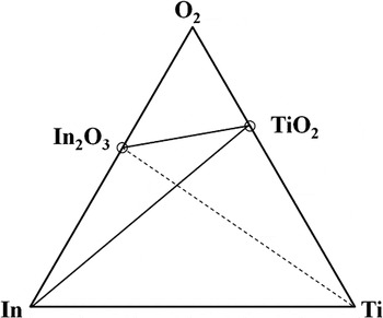
The ternary systems that we are interested in consist of two metals, their oxides, and oxygen. For example, the Ti on In2O3 ternary system consists of the gas phase (oxygen) plus four condensed phases: In2O3, TiO2, Ti, and In. It is useful to represent these phases (neglecting any solid solubility) schematically on a Gibbs triangle as shown in Fig. 1. The Gibbs phase rule tells us that no more than three phases may coexist at equilibrium in a ternary system so we can immediately draw the In2O3–TiO2 tie-line. The field of most interest to interface stability is the one that includes the four condensed phases In2O3, TiO2, Ti, and In, which must have either a tie-line connecting In2O3 to Ti (shown as a dotted line) or one connecting In to TiO2 (shown as a solid line). To determine which tie-line is thermodynamically favored, the two possible tie-line reactions are written in the form of a balanced chemical reaction:

A conventional molar equilibrium In–Ti–O2 ternary phase diagram plotted on the standard Gibbs triangle at 200 °C.

and the reaction Gibbs free energy is found by summing the formation energies of the oxides times their stoichiometric coefficients:  . Since the reaction Gibbs free energy (as written) is negative, the forward reaction direction is favored and we can conclude that the stable tie-line in this system connects In metal to TiO2 and that Ti in contact with indium oxide represents an unstable interface. It is noted that we calculate a standard reaction free energy, which assumes that all the components of the reaction are in their standard state. Condensed phases in their standard state are pure (we assume no interdiffusion), under one atmosphere pressure, and are in their most stable state at the temperature in question. If all the phases are pure, then the only departure from the standard state in this calculation is associated with the amorphous nonequilibrium indium oxide phase, which is likely to have a negligible effect on its formation free energy.
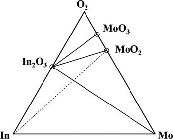
A similar analysis was performed on the In–Mo–O2 ternary system and is shown in Fig. 2. When the competing tie-line reactions are written:

A conventional molar equilibrium In–Mo–O2 ternary phase diagram plotted on the standard Gibbs triangle at 200 °C.

The free energy of the reaction is positive, which indicates that the Mo–In2O3 tie-line (solid line in Fig. 2) is favored over In–MoO2 (dotted line in Fig. 2), and the interface formed when Mo metal is deposited on In2O3 is thermodynamically stable. Note that there are two possible molybdenum oxide phases, MoO2 and MoO3. The trioxide is the phase in equilibrium with oxygen gas, and both the dioxide and the trioxide Mo phases have stable pseudobinary tie-lines to In2O3.
The effect of an unstable interface like Ti on In2O3 on the performance of a Ti-metallized IZO device that is annealed at relatively low temperatures will depend on the kinetics of the reaction and the various competing processes of Ti, O, and O vacancy diffusion in the IZO. Below, we illustrate the effect of metallization on the stability of the a-IZO phase and show that, in the case of a reacting system like Ti on a-IZO, the interfacial reaction can have a profound effect far from the metal edge.
B. Annealing metallized a-IZO: Reaction products
The Ti–a-IZO interface has been shown previouslyReference Lee and Paine27 to react upon annealing at 200 °C to form a thin interfacial TiO2 layer. While the resulting interfacial oxide is thin, the reaction to form TiO2 extracts oxygen from the IZO and therefore injects oxygen vacancies into the underlying a-IZO. The consequence of oxygen vacancy injection is 2-fold; first, since doubly charged oxygen vacancies are electron donors in indium oxide, the carrier density in the vicinity of the reaction front increases. Second, the increased free volume in the film provided by the injected vacancies is likely to affect the rate of crystallization of the amorphous material.
The effect of a reacting Ti–IZO interface on the amorphous to crystalline transformation was studied in a series of in situ TEM heating experiments. In these experiments, the background oxygen pressure is low (P T ∼ 10−6 Torr) and so the metal oxide can only form by reaction with the underlying IZO. The temperature ramp rate of the heating holder is fast (10’s of degrees/s) but the temperature is measured by thermocouple at a location that is close to the heating element and remote from the region under study and so is likely to overestimate the temperature near the center of the TEM sample. Consequently, the temperatures mentioned below are nominal and likely overestimate the actual temperature.
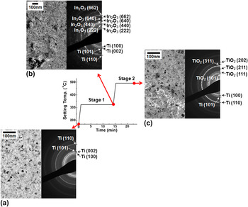
Bright field TEM images were acquired along with corresponding selected area diffraction (SAD) patterns as a function of time at temperature. Figures 3(a)–3(c) shows the nominal temperature cycle and the resultant evolution of the film microstructure as a function of time at temperature. The as-deposited microstructure is shown at time equal zero [part (a)] and shows the fine-grained (∼15 nm) equiaxed polycrystalline microstructure of sputter-deposited metallic Ti. The bright field image shows no contrast from the underlying a-IZO and the SAD pattern is indexed as metallic hcp Ti. A faint broad amorphous ring from the a-IZO is also barely visible in this image but is made difficult to discern by the overlapping Ti (100), (002), and (101) rings. The sample was then heated in the microscope for 15 min at 320 °C and the resulting microstructure is shown in Fig. 3(b). Examination of the bright field image reveals that the polycrystalline Ti is essentially unchanged, but, superimposed on the fine-grained polycrystalline Ti microstructure, there are larger regions of bright/dark contrast that include bend contours (top left field of the image) and areas of dark contrast (bottom left field of the image) indicating a strongly diffracting similarly oriented crystalline region characteristic of larger grained polycrystalline material. Examination of the SAD pattern reveals that the underlying a-IZO has undergone crystallization to the bixbyite crystalline form, which, due to its larger grain size, appears in the SAD pattern as discrete spots among the continuous Ti diffraction rings. There is no evidence of TiO2 in either the diffraction pattern or the bright field image but it is assumed to be present as a thin interfacial layer between IZO and Ti. To demonstrate the formation of significant amounts of TiO2 in reasonable time in the microscope, the sample temperature was increased to 470 °C. The resulting microstructure is presented in Fig. 3(c) and shows that most of the fine-grained Ti metal contrast remains; however, regions of white contrast visible in the bottom half of the bright field image are also visible. The SAD pattern in Fig. 3(c) reveals that the entire layer of a-IZO has been consumed as the previously present crystalline In2O3 is absent from the diffraction pattern and has been replaced by TiO2.
In situ heating TEM analysis shows the morphology of reaction and reaction phase of (a) as-deposited state, (b) stage 1 annealed at ∼320 °C (nominal), and (c) stage 2 annealed at ∼470 °C (nominal).

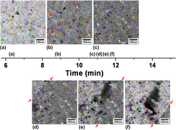
A more detailed view of the a-IZO crystallization is presented in Figs. 4(a)–4(f) where the evolving microstructure is shown at various points [labeled (a)–(f)] on a 6–15 min time line. After 6 min at 320 °C, the microstructure [Fig. 4(a)] is unchanged from the as-deposited structure shown in Fig. 3(a): fine-grained polycrystalline sputtered Ti metal. The microstructure remains largely unchanged after 9 min at 320 °C [Fig. 4(b)] except for the appearance of small (<10 nm) regions of bright white contrast. These regions of white contrast are assumed to be TiO2 reaction product at the interface between Ti and a-IZO but they do not appear as a separate phase in the SAD pattern, possibly suggesting (this is under study) an amorphous form of TiO2. Part (c) of Fig. 4 shows the same region as part (d) separated by only a few seconds. Part (d), however, shows a region of slightly brighter contrast that appears in the upper left hand corner of Fig. 4(d) and is separated from the rest of the sample by a line (marked with arrows) running diagonally across the image. This interface can be seen to remain straight and moves diagonally across the field of view from the upper left to the lower right corner [Figs. 4(e) and 4(f)] at a rate of ∼7 nm/s. Diffraction analysis reveals that this moving boundary separates crystalline IZO from a-IZO and shows, in this example, that nucleation occurred out of the field of view and proceeded by the lateral (as opposed to through thickness) movement of an amorphous–crystalline phase boundary. This same lateral crystallization mechanism, with widely spaced nucleation centers and similar large-grained microstructure, has been reportedReference Paine, Whitson, Janiac, Beresford, Yang and Lewis12 for the crystallization of amorphous indium oxide.
Bright field TEM images (a–f): detailed process of the crystallization of a-IZO metallized with Ti in the stage 1.

The complete crystallization of a-IZO in 15 min at 320 °C shown above is unexpected since it occurs at much lower temperatures than previous studies have reportedReference Yaglioglu, Yeom and Paine1, Reference Jung, Seo, Lee and Jeon13. It is also a matter of technological interest since many In2O3-based AOS TFT fabrication processes include a postprocess anneal in the range 200–400 °C. These postdeposition anneal steps are intended to improve field-effect mobility, subthreshold slope, and channel–metallization contact resistance. We speculate that the crystallization kinetics of a-IZO are enhanced by the injection of oxygen vacancies via:

which provides free volume to allow local tetrahedral Zn–O atomic rearrangement in the octahedral In–O network and hence more rapid transformation rates.
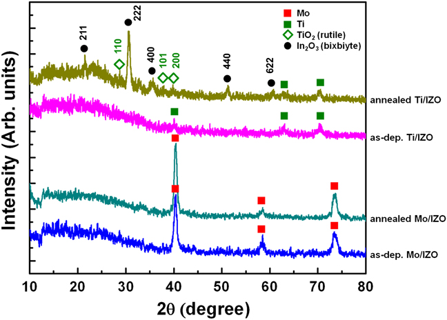
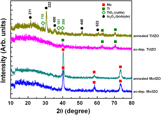
TEM studies of Mo-metallized a-IZO reveal no changes in interface or film microstructure after annealing under similar conditions. Figures 5(a) and 5(b) shows SAD patterns taken from the Mo/IZO bilayer samples in the as-deposited state (left side) and after annealing for 20 h at 200 °C (right side) show no change. There is no change in the Mo diffraction pattern with annealing and there is no evidence that the a-IZO has undergone crystallization. Figure 5(c) shows a bright field plan view TEM image of the annealed Mo/IZO bilayer that includes contrast due to the fine-grained polycrystalline Mo layer and no underlying diffraction contrast that would suggest crystallization of the underlying a-IZO layer. This result was confirmed using GIXRD and results from identically treated Ti-metallized samples are shown in Fig. 6. These results show that the Mo-metallized samples remain unchanged, whereas the Ti-metallized IZO sample shows characteristic crystalline bixbyite peaks and rutile TiO2 after annealing at 200 °C for 20 h in air.
SAD patterns of Mo/IZO bilayers before and after annealing at 200 °C for 20 h in air (a) as-deposited and (b) annealed using camera length of 440 mm and (c) bright field image of 200 °C annealed Mo/IZO sample.

GIXRD patterns of Mo/IZO and Ti/IZO bilayers before and after annealing at 200 °C for 20 h in air.
C. Ex situ AFM and TEM analysis of the near-edge channel region in Ti-metallized IZO
If an interface reaction is self-limiting and the reaction does not proceed laterally, the effect of an unstable interface may be limited to an increase in specific contact resistance. If, however, the reaction is accompanied by lateral growth from the contact into adjacent regions, like, for example, the channel in a gate down TFT, the potential device failure modes increase. To investigate lateral changes in morphology due to a reacting Ti/IZO interface, a 20-nm-thick a-IZO film was deposited onto thermally oxidized Si (SiO2/Si) and then half-covered with a shadow mask to create a metallization edge (Ti 20 nm) to simulate the edge of a TFT source–drain contact in a gate down TFT. The goal was to determine if the effect of Ti metallization and consequent reaction spreads laterally into the channel region of a gate down TFT.
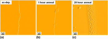
The metal edge regions of Ti on a-IZO samples in the as-deposited condition and after annealing in air for 1 and 20 h were examined using noncontact amplitude mode AFM. Figure 7(a) shows an AFM image of the surface topography of the as-deposited Ti/IZO bilayer with Ti on the left side, a-IZO on the right, and the 20-nm step edge running vertically down the center of the figure. Both the Ti and IZO surfaces are featureless at the scan area resolution used in this work. The result of annealing at 200 °C for 1 and 20 h on the near-edge surface morphology is shown in Figs. 7(b) and 7(c), respectively. As can be seen in these figures, circular bumps about 0.1 μm in diameter and ∼50 nm in height appear after 1 h in isolated locations along the Ti step edge [Fig. 7(b)] and appear everywhere along the edge and spread laterally 3–5 μm from the edge into the IZO after 20 h [Fig. 7(c)].
AFM images obtained near the edge of Ti metallization of (a) as-deposited, annealed in air at 200 °C for (b) 1 h and (c) 20 h.

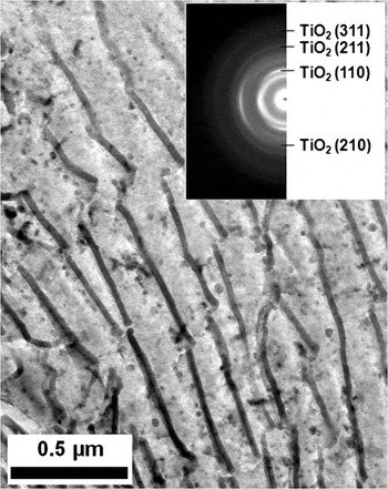
To identify the phase responsible for the near-edge morphology seen in Fig. 7(c), TEM liftoff samples were prepared using similarly prepared and treated samples (20-nm-thick half Ti on 20-nm-thick IZO annealed for 20 h at 200 °C) and were examined. A typical bright field TEM image of the near-edge structure and an indexed SAD pattern is shown in Fig. 8 and shows rod-type crystallographic features that were determined to be the rutile phase of TiO2. An indexed SAD diffraction pattern is presented in the Fig. 8 inset. This ex situ TEM analysis combined with the AFM results show that the TiO2 reaction product is not limited to the Ti–IZO interface but can extend laterally from the metal edge. It may be noted that in these 20 nm/20 nm Ti/IZO samples, there is excess Ti and so the lateral growth can occur either during the interfacial reaction or after the IZO under the Ti metallization is completely consumed. In any case, this Ti/IZO reaction will create a flux of oxygen vacancies that either form voids (none were observed by TEM) or are injected into the underlying IZO. Since doubly ionized oxygen vacancies are double donors, they will provide two free carriers in IZO and the injection of these point defects may lead to significant lateral variations in carrier density in the channel adjacent to the Ti-metallized source–drain region. Such a change in carrier density will shift threshold voltage to the negative bias direction and increase TFT off current.
Bright field TEM image on the reaction region of TiO2 produced by 200 °C anneal for 20 h in air and the associated SAD pattern (inset).

D. General comments on a-I(G)ZO metallizations
The list of a-I(G)ZO metallization candidates that form a thermodynamically stable interface can be rapidly narrowed by using published standard Gibbs free energy data to calculate the free energy of reaction between different candidate metals and indium oxide to form the metal oxide product and indium metal. Table I lists 16 different metals and their standard reaction free energy with In2O3 arranged in order from most negative to most positive  . Of the 16 metals listed, 6 (W, Mo, Sn, Ni, Cu, and Ag) have a positive free energy of reaction with In2O3 and therefore are expected to have a thermodynamically stable metal–In2O3 interface. It should be noted that, for convenience, only the standard reaction Gibbs free energy (
 ) is listed in Table I. The conventional definition of a standard reaction requires that all the components are in their standard state at the temperature in question. The a-IZO that is the focus of this discussion is not in its standard state first because it is not pure (thermodynamic activity is not unity) and, second, because it consists of the amorphous phase rather than the more stable crystalline bixbyite phase. The difference in formation free energy between crystalline and a-In2O3 is not known but is, we assume, negligible since the In–O coordination structure of a-In2O3 is very similar to that of the crystalline bixbyite phase.Reference Paine, Whitson, Janiac, Beresford, Yang and Lewis12 Correction of the standard free energy of reaction for components that are not in their standard state is found by simply adding the activity product as shown below:

Electrical resistivity (ρ) and work function (Φm)Reference Riviere and Green30, Reference Hölzl, Schulte and Höhler31 of potential IZO metallization materials and associated standard Gibbs free energy of reaction ( ) for the formation of oxide via reaction with In2O3 (
 = −744.9 kJ/mol) at 200 °C.

where R is the gas constant, T is the reaction temperature in Kelvin, and a is the activity of each of the components. Activities of pure condensed phases including In (a In), the metal (a M), and the oxide reaction product (a P) are each unity and the activity of the In2O3-rich In2O3–ZnO oxide solid solution is assumed to be ideal [i.e.,  = 0.763 = mol% of In2O3 in IZO (90 wt% In2O3–10 wt% ZnO)] as is typical for the solvent in a rich solution. The resulting calculation reveals that the nonstandard ΔGrxn is only approximately 1.063 kJ/mol larger/smaller than the tabulated
 values and does not change the predicted result.
Examination of Table I shows that  of ZnO with In metal is −133.7 kJ/mol. Its location adjacent (and to the left of) the transition from stable to unstable interfaces means that pure metallic Zn will react with In2O3 to form ZnO but all the metals to the left of Zn will reduce ZnO to Zn metal and all the metals to the right of the Zn column, including In2O3, will be stable on ZnO. It is, therefore, possible (depending on the activity of ZnO) that Zn reduction may also occur in the reactive interface cases discussed above though metallic Zn was not observed in this study.
It is noted that many metals that are widely used in modern Si-based microelectronics, like Al and Ti, are not thermodynamically stable in the IZO system. Of course, kinetic constraints may allow the use of some metals with thermodynamically unstable interfaces if the maximum processing temperature is sufficiently limited. For example, some reactive metals may only form a thin continuous interfacial oxide whose growth self-terminates if transport through the product oxide [of either the metal to the I(G)ZO or oxygen from the I(G)ZO to the metal] is slow. However, even a relatively thin interfacial oxide is likely to result in increased contact resistance.
In selecting optimum candidate materials for the metallization of In-based AOSs, there are additional considerations beyond interface stability. These include specific contact resistance of the metal–AOS interface and metal resistivity. Table I lists, for each of the 16 candidate metals, published values for electrical resistivity and work function (Φ). Low resistivity is an obviously important characteristic for metallization materials. Similarly, the work function difference (Φms = Φm−ΦIZ(G)O) must be small to minimize the electron barrier height and to form good ohmic contact. This occurs when the work function of the metal is approximately the same as, or slightly lower than, that of I(G)ZO (∼4.6–4.8 eVReference Shimura, Nomura, Yanagi, Kamiya, Hirano and Hosono18). The work function of five (W, Mo, Sn, Cu, and Ag) of six thermodynamically stable metals is close to that of ΦI(G)ZO and, hence, these five metals are promising candidates for the formation of thermodynamically stable low contact resistance contacts to I(G)ZO.
IV. SUMMARY
The rapid progress in the development of In2O3-based AOS TFT’s has led to a need for improved fundamental understanding of the materials science of AOS metallization. The first step in this improved materials understanding is in determining the thermodynamic stability of any metallization approach that might be used. We have shown that a basic thermodynamic analysis can be used to predict the interface stability of potential I(G)ZO metallization materials. Two widely used AOS TFT metallization materials were selected, Mo and Ti, and the stability of their interfaces with In2O3 was calculated and then examined experimentally on a-IZO. It was found that Ti reacts with a-IZO at 200 °C to produce crystalline rutile TiO2 both at the Ti–IZO interface and laterally away from the step metal edge (into the channel region). Furthermore, the Ti–IZO reaction results in a significant drop in the temperatures at which crystallization of a-IZO occurs at observable rates (from 500 to 200 °C). In contrast, based on its standard free energy of reaction with In2O3, Mo is predicted and experimentally shown to have a thermodynamically stable interface. a-IZO remained amorphous on annealing at 200 °C for 20 h and no reaction oxides were detected or predicted.
ACKNOWLEDGMENT
The authors gratefully acknowledge the financial support of the National Science Foundation (NSF) Award No. DMR-0804915.