I. INTRODUCTION
For the production of microelectronic devices, like printed circuit boards, radio-frequency identification (RFID) tags,Reference Huang, Liao, Molesa, Redinger and Subramanian1,Reference Fuller, Wilhelm and Jacobson2 and organic photovoltaics, microstructured conductive patterns are required. Physical vapor deposition or sputtering techniques are commonly used for the fabrication of conductors but are incapable of selective patterning.Reference Reinhold, Hendriks, Eckardt, Kranenburg, Perelaer, Baumann and Schubert3 Other patterning techniques, like photolithography and laser patterning, require expensive masks and are highly time-consuming processes—both strongly increasing the production costs when a small number of samples is required. To produce disposable flexible electronics on cost-effective polymeric substrates, it is crucial to change to techniques that are roll-to-roll (R2R) compatible.Reference Søndergaard, Hösel and Krebs4 Prospective patterning techniques suitable for R2R processing, which were already used for the preparation of RFID antennas are, e.g., screen printing,Reference Shin, Lee and Kim5 flexography,Reference Kowalik, Worch, Hartwig and Joachimi6 and inkjet printing.Reference Perelaer, Smith, Mager, Soltman, Volkman, Subramanian, Korvink and Schubert7 Although traditional printing techniques as screen printing or flexography are using a permanent printing form to transfer the ink to the substrate, inkjet printing as a full digital nonimpact printing method creates patterns directly on-demand without requiring such physical printing forms. Hence, the patterns can be instantly adapted to specific requirements of a wide variety of applications. Finally, inkjet printing is an environmentally friendly and a cost-effective patterning method since the material is placed on-demand with minimal waste generation.Reference Søndergaard, Hösel and Krebs4,Reference Perelaer, Smith, Mager, Soltman, Volkman, Subramanian, Korvink and Schubert7
Inkjet printing of conductive precursor materials has been used frequently for the production of conductive features during the last years. As precursor materials, both metal-organic decomposition (MOD) and metallic nanoparticle (NP) inks have been used.Reference Smith, Shin, Stringer, Derby and Reis8,Reference Kamyshny, Steinke and Magdassi9 Each type of ink has advantages as well as disadvantages. For example, MOD inks are solutions, which reduce nozzle clogging, and do not require colloidal stabilizers, whereas NP inks, usually have a higher metal loading, are more widely commercially available and have been reported as having lower contact resistances.Reference Perelaer, de Laat, Hendriks and Schubert10,Reference Gamerith, Klug, Scheiber, Scherf, Moderegger and List11
After evaporation of the solvent, both types of inks require a posttreatment step to render the precursor materials conductive.Reference Perelaer, Smith, Mager, Soltman, Volkman, Subramanian, Korvink and Schubert7 In the case of an MOD ink, a reduction of the metal in the metal-containing complex takes place. For an NP ink, the organic capping agent that protects the NPs from agglomerating in solution is removed. Once the organic materials are removed or decomposed from the surface, the particles make direct physical contact, resulting in a continuous and conductive network throughout the printed feature.Reference Perelaer, de Laat, Hendriks and Schubert10 Neck formation between the particles takes place through Sintering—a process whereby the surface energy is reduced due to the minimization of the particles’ surface-to-volume ratio and, as a consequence, the conductivity increases rapidly.Reference Goeke and Datye12 Furthermore, larger particles are formed due to particle migration and coarsening (Ostwald ripening).Reference Perelaer and Schubert13 During sintering, the relative density increases with increased temperature or pressure and decreases with increased particle size.Reference Kang14 The sintering process is commonly activated by heat and for sintering silver NPs, typically temperatures >150 °C are required.Reference Fuller, Wilhelm and Jacobson2,Reference Lee, Chou and Huang15 However, it is crucial that the processing temperature remains below the glass transition temperature (T g) of the polymeric substrate, otherwise, the substrate could become permanently deformed.Reference Perelaer and Schubert13 Therefore, thermal sintering using temperatures >150 °C is not compatible with cost-effective polymer foils, such as polycarbonate (T g = 148 °C) and polyethylene naphthalate (T g = 120 °C), which are typically used as substrates for flexible electronics.Reference Perelaer, Jani, Grouchko, Kamyshny, Magdassi and Schubert16,Reference Kim, Dhage, Shim and Hahn17 Various approaches have been reported during the last years to lower the sintering temperature of NP inks.
First, the NP inks were tailored to significantly lower the amount of organic additivesReference Perelaer, Smith, Mager, Soltman, Volkman, Subramanian, Korvink and Schubert7 or by adding a sintering agent, such as a chloride-containing salt.Reference Grouchko, Kamyshny, Mihailescu, Anghel and Magdassi18,Reference Tang, He, Zhou, Wang, Yang, Tao and Zhou19 A serious drawback of using a low content of binding materials is that the resulting ink is difficult to inkjet print. Organic binders promote the inks printability and are often added to assure mechanical integrity and adhesion to the substrate.Reference Perelaer, Smith, Mager, Soltman, Volkman, Subramanian, Korvink and Schubert7
A different approach is to selectively sinter the NP inks, e.g., by intense pulsed light,Reference Kim, Dhage, Shim and Hahn17,Reference Hosel and Krebs20,Reference Angmo, Larsen-Olsen, Jørgensen, Søndergaard and Krebs21 a laser beam,Reference Ko, Pan, Grigoropoulos, Luscombe, Frechet and Poulikakos22,Reference Bieri, Chung, Poulikakos and Grigoropoulos23 a DC,Reference Allen, Aronniemi, Mattila, Alastalo, Ojanpera, Suhonen and Seppa24,Reference Leppaniemi, Aronniemi, Mattila, Alastalo, Allen and Seppa25 microwaves,Reference Roy, Agarwal, Chen and Gedevanishvili26,Reference Perelaer, de Gans and Schubert27 and a low-pressure plasmaReference Reinhold, Hendriks, Eckardt, Kranenburg, Perelaer, Baumann and Schubert3 and an atmospheric plasmaReference Wunscher, Stumpf, Teichler, Pabst, Perelaer, Beckert and Schubert28 or a combination of techniques.Reference Perelaer, Jani, Grouchko, Kamyshny, Magdassi and Schubert16,Reference Perelaer, Abbel, Wünscher, Jani, van Lammeren and Schubert29 Although most of these techniques have been demonstrated only on the lab scale so far,Reference Reinhold, Hendriks, Eckardt, Kranenburg, Perelaer, Baumann and Schubert3,Reference Perelaer, de Gans and Schubert27,Reference Wunscher, Stumpf, Teichler, Pabst, Perelaer, Beckert and Schubert28 photonic sintering is already shown to be capable for production processes like R2R production.Reference Hosel and Krebs20,Reference Angmo, Larsen-Olsen, Jørgensen, Søndergaard and Krebs21 An attractive candidate for large area sintering is, however, also plasma sintering, as substrate sizes up to A4 paper size (210 × 297 mm) can be uniformly exposed at once. Plasma exposure causes the decomposition of the organic moieties around the NPs within the printed feature from top to bottom resulting in a skin layer, which is growing gradually.Reference Reinhold, Hendriks, Eckardt, Kranenburg, Perelaer, Baumann and Schubert3 After a sufficient amount of sintering time, the as-printed features are converted into a contiguous particle network.
Low-pressure argon plasma sintering usually suffers from long processing times, as the process proceeds from top to bottom, and therefore, only thin layers of a few 100 nm can be processed in reasonable periods. Besides the layer thickness, the sintering time depends on the thermal stability of the metal precursor ink. In a previous study, it was shown that an ink with a low thermal stability, hence sinters at a low temperature, is beneficial for the plasma sintering process. Electrical conductivities up to 30% of bulk silver have been obtained but required sintering times of ≥60 min.Reference Reinhold, Hendriks, Eckardt, Kranenburg, Perelaer, Baumann and Schubert3 Recently, it was shown that an electrical conductivity of >40% was possible by combining plasma and microwave sintering. In that case, a plasma presintering step was used to introduce a moderate conductivity into the as-printed features, which triggers the subsequent microwave sintering process.Reference Perelaer, Jani, Grouchko, Kamyshny, Magdassi and Schubert16
In this contribution, the rapid low-pressure argon plasma sintering of a tailored silver NP ink is presented, yielding a conductivity of up to 40% of bulk silver without exceeding a process temperature of 70 °C. The plasma sintering process is compared with conventional thermal sintering and demonstrated to be applicable for inkjet-printed silver antennas for RFID tags.
II. EXPERIMENTAL SECTION
A. Inkjet printing and sintering
Silver NP dispersions in a mixture of high boiling point solvent (200–250 °C) and a low boiling point solvent (<100 °C) were provided by Agfa-Gevaert N. V. (Mortsel, Belgium). The silver inks contain 14–17 wt% of silver NPs with an average particle diameter of 20–30 nm. Inkjet printing experiments were performed by using a piezoelectric Dimatix Materials Printer (DMP 2831, Fujifilm Dimatix, Lebanon) equipped with a 10 pL printhead (DMC-11610, 16 nozzles, 21.5 μm nozzle diameter). The inks were printed at a voltage of 28 V and a pulse duration of 2.5 μs, using a frequency of 1 kHz and a customized waveform. The nozzle plate was set to 28 °C, whereas the substrates were kept at room temperature.
Glass slides (Marienfeld, Lauda-Königshofen, Germany) were used as substrates, which were cleaned by washing with isopropanol and dried under flow of nitrogen. For the conductivity measurements, lines with a length of 15 mm and a width of approximately 100 μm (3 pixels) were printed with a resolution of 900 dpi. The RFID antennas were printed with a resolution of 1270 dpi on a crosslinked polyethylene terephthalate foil (PET, Thermoline PET-V109, Agfa-Gevaert N. V., Mortsel, Belgium, 120 μm thick, T g = 140 °C).
Plasma sintering was performed using a low-pressure argon plasma instrument (Nano, Diener electronic GmbH & Co. KG, Ebhausen, Germany). Argon was used as a process gas, and the working pressure, reached after approximately 7 min of pumping, was 0.2–0.4 mbar. Lines were sintered at a power of 150 and 300 W, whereas the RFID antennas were sintered at 300 W. Reference antennas were prepared by screen printing a standard available paste (Du Pont 5029, Du Pont de Nemours GmbH, Neu-Isenburg, Germany) using a flatbed screen printer.
B. Characterization
Thermogravimetric analyses (TGA) were performed with a TG50 by Mettler Toledo under ambient atmosphere in the range from 40 to 650 °C with a heating rate of 10 K/min. First, the samples were kept at 40 °C for 2 h to remove the low boiling point solvent. Resistivity was determined by attaching the electrodes of a multimeter (Voltcraft Digital Multimeter VC-960, Conrad Electronics GmbH, Hirschau, Germany) to the leaderbar of each printed sample via conductive pads from a conductive silver paste (Ferro GmbH, Hanau, Germany) and measuring the resistance via a two-point measurement setup. Then the resistivity was calculated using the measured resistance and the dimensions of the leaderbar obtained by measuring the profile. Scanning electron microscopy (SEM) images were taken using an LEO 1530 Gemini FE-SEM (Carl Zeiss, Oberkochen, Germany). Prior to the measurements, a thin layer of platinum (<10 nm) was sputtered onto the samples using a sputter coater (MED 20 High Vacuum Coater, Bal-Tec AG, Liechtenstein). Surface topography of the inkjet-printed samples was measured with an optical profilometer (Wyko NT 9100, Veeco, Plainview). For the sheet resistance measurements, a four-point setup was used. The measurement was carried out on a conductor path with a length of 10 mm by using a conducting unit (no. E-0028-14-10, Power Paper Ltd, Jerusalem/Israel) in combination with a resistance measurement device (HIOKI 3560 AC mΩ HiTESTER, HIOKI E. E. CORPORATION, Tokyo, Japan). The layer thickness of the screen-printed antenna was measured from a polished cross-section of the structure with a reflected-light microscope (NEOPHOT 2, Carl Zeiss AG, Oberkochen, Germany).
III. RESULTS AND DISCUSSION
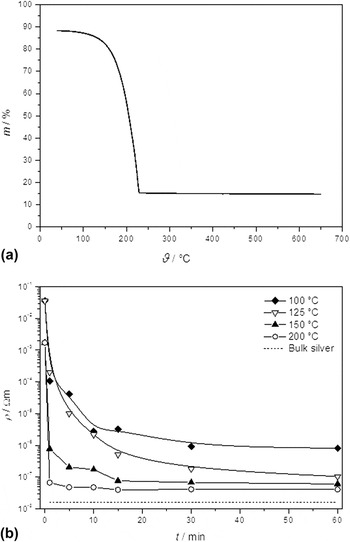
To understand the thermal stability of the solvent-based silver NP ink, the mass decrease upon heating was investigated by TGA [Fig. 1(a)]. After an initial isothermal step at 40 °C for 2 h, a decrease of 11.7 wt%, corresponding to the low boiling solvent, was observed. The TGA curve then shows a decrease of 73.6 wt%, which corresponds to the high boiling solvents as well as to the organic binder. A gradual decrease and a single deflection point in the graph indicate that the solvents and the organic binder are removed simultaneously. Above 230 °C, all volatile components are removed from the ink.
TGA (heating rate = 10 K/min) of the silver NP ink (a). Resistivity as a function of sintering time and temperature for thermal sintering of inkjet-printed silver NPs (b).

Next we studied the thermal sintering performance of the ink. Simple line structures (15 mm × 100 μm) were inkjet printed on glass substrates and subsequently sintered thermally. Figure 1(b) shows the resistivity of the inkjet-printed lines as a function of sintering time and temperature. The dashed line in Fig. 1 indicates the bulk silver resistivity (1.6 × 10⁻⁸ Ω m). As expected, the resistivity decreases with time and decreases faster if higher temperatures are applied. After 15 min of sintering at 100 °C, the resistivity is approximately two to three orders of magnitude greater than for bulk silver. Improved resistivity values were observed at temperatures ≥150 °C, but these temperatures are not suitable for cost-effective polymer foils like polycarbonate or polyethylene naphthalate, which have a T g < 150 °C. Moreover, sufficiently fast sintering compatible with R2R processing was only achieved at 200 °C, where after 1 min, a resistivity of 6.7 × 10⁻⁸ Ω m was obtained. The lowest resistivity of 4.0 × 10⁻⁸ Ω m was achieved by thermal sintering after 15 min at 200 °C, corresponding to a conductivity of 40% of bulk silver. The resistivity did not decrease further with longer sintering time.
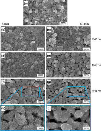
Figure 2 and Supporting Information Fig. 1 show, respectively, top view and cross-sectional SEM images of the inkjet-printed lines before and after sintering. It can be seen that the NPs agglomerate when printed and dried at room temperature [see Fig. 2(a)]. Upon sintering at 100 °C, the NPs are densified, but neck formation is not observed after 5 and 60 min of sintering [Figs. 2(b) and 2(c)]. Applying a temperature of 150 °C resulted in significant neck formation [Fig. 2(d)] and after 60 min, a raspberry-like fine structure was revealed [Fig. 2(e)]. At 200 °C, a porous structure can be seen after 5 min, see Fig. 2(f) and for a higher magnification in Fig. 2(h). The final stage of sintering was reached after 60 min [Fig. 2(g)], indicated by the low number of observable individual NPs, which is better visible in the higher magnified image in Fig. 2(i). The dense network confirms the low resistivity after 60 min of sintering, but the large pores limit the final conductivity to less than that of bulk silver.
Scanning electron microscopy (SEM) images of inkjet-printed silver NPs at room temperature (a) and after thermal sintering at 100 °C (b, c), 150 °C (d, e), and 200 °C (f–i). The images in the left and right column represent a sintering time of 5 and 60 min, respectively.

The final conductivity of 40% after sintering for 15 min at 200 °C is promising for microelectronic applications that require a high conductivity.Reference Perelaer, Smith, Mager, Soltman, Volkman, Subramanian, Korvink and Schubert7 The sintering temperature is, however, too high for cost-effective polymer foils that are frequently used for printed electronics applications. Therefore, we switched to a more temperature-friendly sintering method while taking a fast sintering into account.
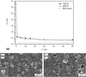
Figure 3(a) shows the resistivity as a function of time for power of 150 and 300 W. Whereas plasma sintering is typically a slow sintering method, due to the top to bottom evolution of the process, the process here shows a rapid decrease of the resistivity within the first minute of sintering. Within the first minute of sintering at 150 W, a resistivity of 14 × 10−8 Ω m was obtained (≈11.4% of the bulk silver conductivity), while after 10 min, the conductivity increased to 16.5% of the bulk value. In the case of thermal sintering, such conductivity would require 15 min of sintering at 150 °C. However, the temperature during plasma sintering did not exceed 70 °C,Reference Perelaer, Jani, Grouchko, Kamyshny, Magdassi and Schubert16 which is well below the T g of the polymer substrate used for the preparation of RFID antennas (crosslinked PET foil, T g = 140 °C). When sintered at 300 W, conductivity as high as 40.2% of bulk silver was obtained after 60 min of plasma exposure.
Resistivity as a function of sintering time and power for plasma sintering of inkjet-printed silver NPs (a). Scanning electron microscopy (SEM) images of inkjet-printed silver NPs after plasma sintering at 300 W for 5 min (b) and 60 min (c), respectively.

Figures 3(b) and 3(c) show top-view SEM images of inkjet-printed lines that were plasma sintered at 300 W for 5 and 60 min, respectively. It can be seen that the NPs have merged into a continuous structure with low porosity, explaining the low resistivity of 9.5 × 10⁻⁸ Ω m already after 5 min. The lowest resistivity was 4.0 × 10⁻⁸ Ω m after 60 min sintering. Interestingly, the porosity is similar for both sintering times, which indicates that the initial state of sintering the NPs, i.e., the removal of the organic stabilizing material, is a fast process followed by the densification of the material.
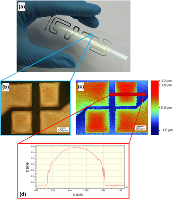
To demonstrate the applicability of the presented rapid low-pressure plasma sintering process of this tailored ink for the production of flexible electronics, RFID tags were prepared. Antenna structures were inkjet printed onto PET foils with a resolution of 1270 dpi. The resolution was higher for the sintering experiments on glass, which was required to overcome the suboptimal wetting properties of the ink on the polymer substrate and to obtain continuous structures. A photograph of such an antenna is shown in Fig. 4(a). Subsequently, the antenna structures were plasma sintered at 300 W. By sintering for 10 and 60 min resistivities between 13.2 × 10⁻⁸ and 5.4 × 10⁻⁸ Ω m were obtained, being equal to conductivities of 12.0% and 29.5% of bulk silver, respectively. Since the antenna structures were inkjet printed at a resolution of 1270 dpi instead of 900 dpi, resulting in a thickness of approximately 300 and 550 nm for 1 and 2 layers, respectively, the resulting conductivities are lower than those obtained in previous experiments with thicknesses of 50–100 nm, where 24.4% and 40.0% of the bulk silver conductivity were achieved after 10 and 60 min, respectively. This originates from the fact that plasma sintering proceeds from the top to bottom of the structure and the formed crust acts as a kind of barrier for the plasma species and therefore decelerates the sintering of the subjacent material. Microscopic as well as white light profiler images of the chip position of the antenna are shown in Figs. 4(b) and 4(c), respectively. Both images confirm a good and uniform printing quality, indicated by a sharp edge of the four building blocks of the structure as well as the absence of the coffee ring effect.Reference Deegan30
Inkjet-printed RFID antenna on PET foil: photograph of the antenna (a), a light microscope image (b), and a top-view (c) and cross-sectional (d) white light profiler image of the chip position after sintering.

After successfully manufacturing the antenna structures, the functionality of the RFID antennas was tested. Each antenna was equipped with a UHF transponder chip (complete unit is called label or tag) and then placed in a measuring cell of 1 m,Reference Reinhold, Hendriks, Eckardt, Kranenburg, Perelaer, Baumann and Schubert3 which contained a UHF reader at a fixed distance to the label. The RFID tag was then tested by sending 100 sequential signals at 915.25 MHz from the reader to the tag and by recording the resulting number of successful answers. Subsequently, the process was repeated for a systematically varied attenuation of the signal. An overview of the results of the tested samples is summarized in Table I. A number of 100 indicates that all responses from the label to the reader were successful, whereas a lower number results from a few missed responses and zero implies that no response made it back to the transponder. From the table, it can be seen that when sintered at least 30 min, the RFID tags worked without losing the signal once up to an attenuation of 7.65 dB and are comparable with the screen-printed antennas. Note that an antenna that was sintered for 10 min is properly functioning, but upon usage a shorter distance to the reader is required, as the answering signal is weaker. The performance of two-layered antenna samples is superior to the single-layered antennas. This fact is in compliance with the finding of a previous study that higher thicknesses of printed RFID antennas result in better performance characteristics.Reference Merilampi, Bjorninen, Vuorimaki, Ukkonen, Ruuskanen and Sydanheimo31 Although the resistivity remains similar for samples that were plasma sintered for 30–60 min, the trend of increased performance can be clearly followed when looking at the sheet resistance of the inkjet-printed antenna structures; a decreased sheet resistance directly results in a better performance.
Performance of the plasma-sintered RFID antennas in functional tests: the number of responses by the RFID tags at different attenuations of the signal is shown. Characteristics of the printed antennas, including the number of layers, the sintering time, the structure height, the resistivity, and the sheet resistance.

a Sheet resistance values measured at different areas of the antenna samples, average value is reported.
b Resistivity values measured/calculated from the leaderbar of each sample.
c Reference antennas prepared by screen printing and cured at 130 °C in a convection dryer.
The performance of the antennas sintered for at least 30 min is similar to the screen-printed ones, whose thickness is more than 50 times greater than that of the inkjet-printed samples. This indicates that the difference in the structure height is compensated by the low resistivity values of the inkjet-printed antennas obtained by plasma sintering in comparison with the screen-printed ones. The reason why inkjet-printed antennas are preferred to the screen-printed ones is obvious: because of their small thickness, much less material is required and, therefore, the material costs are reduced significantly.
IV. CONCLUSION
A rapid low-pressure plasma sintering process of an inkjet-printed silver NP ink was reported. The solvent-based ink was sintered within 1 min to a conductivity of 11.4% of the bulk silver value. Although the maximum processing temperature did not exceed 70 °C, excellent conductivity values of up to 40% were revealed at longer exposure times.
Fully functional RFID tags prepared with inkjet-printed antennas showed similar results as devices prepared by screen printing. However, the inkjet-printed samples were considerably thinner than the screen-printed samples, while yielding sufficient conductivity for the RFID tags. Therefore, inkjet printing has a great advantage to be a more cost-effective processing technique. Moreover, it was shown that the process of plasma sintering is suitable for preparing printable electronics devices on cost-effective PET foils.
ACKNOWLEDGMENTS
For financial support, the authors thank the Dutch Polymer Institute (DPI, technology area HTE) as well as the European Community’s Seventh Framework Program (FP7/2007–2013) under grant agreement no. 248816. Renzo Paulus, Laboratory of Organic and Macromolecular Chemistry, Friedrich-Schiller-University, Jena, is kindly acknowledged for his assistance with the TGA measurements.