I. INTRODUCTION
In the rapidly growing market of wireless communication, smart antenna technology is an effective tool to enhance performance, coverage, and spectrum reusability. Electronically scanned phased arrays are widely used in radar, satellite, cellular, and various civil and military communication applications. Primary obstacle in wide scale deployment of scanned phased arrays is the high-cost associated with phase shifters, which are a critical element of the T/R modules in these arrays. The phase shifters introduce relative phase shifts among antenna elements of the array for steering the beam in the desired direction. Sometimes the cost of phase shifters is nearly half of the total cost of the phased array.
Electronically steerable parasitic array radiator (ESPAR) is the technique by which beam steering is achieved without the use of phase shifters. In ESPAR antenna, a driven element is surrounded by closely spaced parasitic elements. The parasitic elements are excited by the phenomenon of mutual coupling between the driven and parasitic elements. The parasitic elements are reactively loaded. The desired beam steering/null placement is achieved by controlling the reactance associated with parasitic elements [Reference Lu, Ireland and Schlub1–Reference Chen, Hirata, Ohira and Karmakar3]. For a switched parasitic array antenna, the parasitic elements are open/short circuited with antenna ground plane to achieve switched beam steering [Reference Chen, Sun and Wang4].
A lot of literature is available on switched parasitic antenna arrays [Reference Chen, Sun and Wang4–Reference Li and Feng7]. In [Reference Schlub, Lu and Ohira8], a ground skirted switched beam monopole ESPAR antenna has been designed and analyzed. The non-planar profile of this antenna structure poses difficulties in its integration into mobile terminals. In [Reference Thiel and Smith5], microstrip patch elements have been used; however, the radiation pattern is directed toward broadside limiting its use in wireless systems. Patch antenna elements with seven hexagonal elements and seven circular elements have been investigated in [Reference Shi, Lu and Ireland9]. Switched azimuth steering has been achieved by the use of RF switches and making each antenna element circularly polarized. A circularly polarized antenna used at transmitter dictates the use of an antenna with the same polarization at receiver to ensure minimum polarization mismatch loss and optimum reception. In [Reference Chen, Sun and Wang4], the antenna elements are hexagonal patches. These patches are shorted to the ground plane by metal vias. Coaxial feed for the driven element and loading point of pin diode switch for the parasitic element is located at one side of the metal via. Due to such feeding and loading configuration, the antenna's azimuth radiation patterns are not entirely uniform. However, the antenna is linearly polarized. Utilization of ESPAR antenna in a multiple-input multiple-output (MIMO) system has been investigated in [Reference Zhou, Adve and Hum10]. The pattern reconfigurability has been leveraged for performance enhancement of the MIMO system in an indoor wireless channel.
In this paper, a switched beam planar ESPAR with a unique feeding mechanism has been discussed. The antenna developed has symmetric azimuth/elevation radiation patterns. It is an aperture-coupled antenna; hence, the unique feeding structure and the radiating elements are isolated from each other by the ground plane. Due to such isolation, undesired coupling between antenna elements and feed structure is minimized. Therefore, the antenna can find its wide use in integration with other microwave circuits such as in active integrated antennas. To the author's best knowledge, an aperture-coupled ESPAR antenna with such feeding mechanism has not been discussed in literature before.
II. ANTENNA DESIGN AND IMPLEMENTATION
A) Radiating side
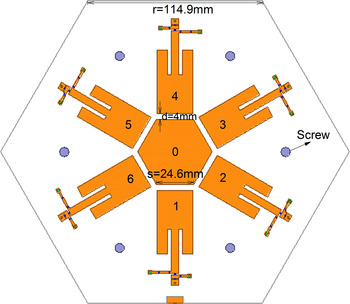
The designed ESPAR antenna is an aperture-coupled antenna. Radiating side of antenna structure along with various dimensions is shown in Fig. 1. The central/driven element labeled as 0 is a hexagonal microstrip patch. It is excited by the feed through a slot in the ground plane. The parasitic elements labeled 1–6 are inset-fed rectangular microstrip patches.
Radiating side of antenna.

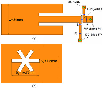
An individual parasitic element is illustrated in Fig. 2(a). The parasitic patch shorts to the ground plane with the help of RF shorting pin if the pin diode is forward biased. Also shown in Fig. 2 are the DC traces, pads, and contacts for biasing of the pin diode. Capacitor (C), resistor (R1), and Inductors (L) are also in place as DC biasing circuit elements for pin diodes and also to isolate the RF signal from DC path and vice versa.
(a) Inset-fed parasitic patch. (b) Slot in ground plane.

B) Slot design
In Fig. 2(b), the slot in the ground plane is shown. Slot is actually an overlap of three concentric equal length rectangular slots. The larger angular separation between any two slots is 120°. Slot, in ground plane, lies exactly below the center of the hexagonal patch.
C) Feed structure
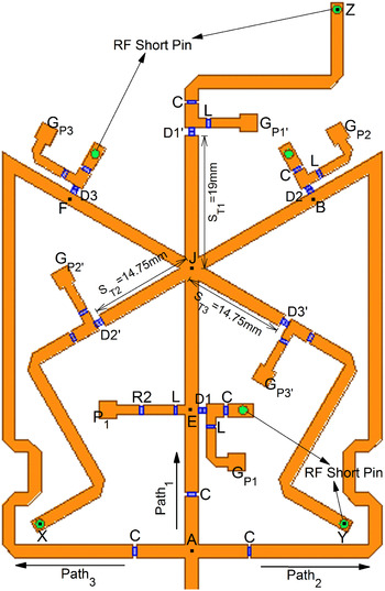
Figure 3 illustrates the feed network. The feed structure has six pin diodes labeled D1, D1′, D2, D2′, D3, and D3′. Various DC traces and pads, capacitors (C), resistor (R2) and inductors (L) are also visible. These are meant for biasing the pin diodes and for RF and DC isolation. Six RF shorting pins are also seen. These RF shorting pins and pin diodes are placed at proper locations for controlling the RF signal to flow over a specific path. The operation mechanism of feed network will be explained shortly.
Feed network.

III. OPERATION MECHANISM
In Fig. 1, the parasitic element which is open circuited acts like a director and the element which is short circuited behaves like a reflector. The central hexagonal element mutually couples to an open-circuited parasitic element. The specific surface current of the driven element that is required to be induced into the parasitic element for useful mutual coupling is excited through the slot by the feed network.
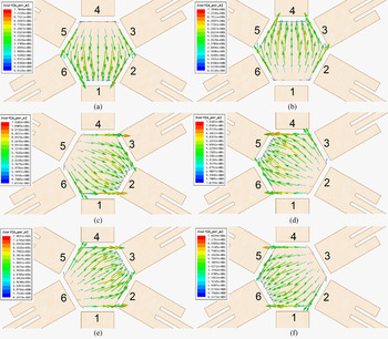
E-plane coupling takes place for elements lying in the E-plane and H-plane coupling takes place for elements lying in H-plane. Parasitic elements 1 and 4 are lying in the E-plane in reference to the surface current of the driven hexagonal patch as depicted in Figs 4(a) and 4(b). The remaining elements (2, 3, 5, and 6) are lying neither in the E-plane, nor in the H-plane. For coupling in the E-plane, surface current which is excited in the hexagonal patch through the slot has to be directed as illustrated in Figs 4(a) and 4(b). Open circuiting element 1 (by reverse biasing its PIN-diode) will result in tilting of the far-field radiation pattern from broadside, in elevation plane, toward this element. This results in steering of the beam toward element 1. All the remaining parasitic elements are short circuited (by forward biasing their PIN-diodes) and act like reflectors in this scenario. If element 4 is open circuited and remaining elements are short circuited, then the beam will be formed in the opposite direction, i.e. toward element 4.
Surface current (Jsurf) for beam steering in various directions. (a,b) Jsurf for beam steering toward elements 1 and 4. (c,d) Jsurf for beam steering toward elements 2 and 5. (e,f) Jsurf for beam steering toward elements 3 and 6.

To form the beam toward element 2 or 5, the surface current has to be excited in such a way that it orients itself toward these two elements only. This surface current is illustrated in Figs 4(c) and 4(d). Same is the case for elements 3 and 6, illustrated in Figs 4(e) and 4(f). This way, a maximum of six switched beam patterns can be achieved. The creation of surface current in various directions is achieved through this special feed network.
A) Operation mechanism of feed network
Operation of feeding network to induce a specific surface current in the driven element is hereby explained. In Fig. 3, feed network is illustrated as viewed when the radiating side of antenna is flipped over. The RF input signal path coming from signal source, at point A, is split into three paths namely Path1, Path2, and Path3. Path1 corresponds to parasitic elements 1 and 4. Path2 corresponds to parasitic elements 2 and 5. Path3 corresponds to parasitic elements 3 and 6. The length from point A to point E is λg/4, where λg is guided wavelength, i.e. wavelength of RF signal in the microstrip line given as λ 0/√ε eff . λ 0 is free space wavelength and ε eff = 2.54 for Taconic TLC-32 substrate of dielectric constant 3.2. λg turns out to be 76.84 mm. The lengths from points A to B and A to F are 5λg/4. At locations of B, F, and E, there are pin diodes as well as RF shorting pins. If forward biased, the PIN-diodes will short the RF signal to the ground plane through their respective shorting pins. The lengths from J to B, J to F, and J to E are equal to λg/4. All the three lengths, i.e. from J to the shorting pin beyond D1′ at Z, to the shorting pin beyond D2′ at X, and to the shorting pin beyond D3′ at Y are equal to 3λg/4. In order to create the surface current as shown in Figs 4(a) and 4(b), RF signal coming from source has to flow through Path1 only from point A. Diodes D1 and D1′ over Path1 are reverse biased. In order to block the signal from flowing into Path2 and Path3, diodes D2 and D3 are forward biased. A transmission line of length an odd multiple of λg/4 terminated by a short circuit presents at its input an open circuit (very high impedance) for an RF signal. Hence, the RF signal at point A sees open circuit toward Path2 and Path3 and the only path left to flow is Path1 and the RF signal reaches point J. There is a junction of all the three paths at point J. Since D2 and D3 are forward biased, for RF signal at point J, again it is an open circuit (very high impedance) toward D2 and D3 and hence the RF signal will not flow over these two paths. Diodes D2′ and D3′ are also forward biased. Since the lengths from point J to the shorting pins beyond D2′ and D3′, at X and Y, respectively, are 3λg/4, again for the RF signal, it is an open circuit (very high impedance) and hence the paths toward D2′ and D3′ are blocked for RF signal to flow. Therefore the length from point J to D1′ (which is reverse biased), i.e. S T1 acts as the only stub for impedance matching as required in a simple aperture-coupled antenna. Henceforth, the RF signal of Path1 excites the hexagonal patch and creates the surface current on it as depicted in Figs 4(a) and 4(b).
To create surface current as shown in Figs 4(c) and 4(d), the PIN-diodes D2 and D2′ will be reverse biased and PIN-diodes D1, D1′, D3, and D3′ will be forward biased. This will cause the RF signal to flow on Path2 only and hence the requisite surface current will be created on the hexagonal patch. The length from point J to D2′, i.e. S T2 will act as impedance matching stub. In order to create the surface current as shown in Figs 4(e) and 4(f), PIN-diodes which will be reverse biased are D3 and D3′ and those which will be forward biased are D1, D1′, D2, and D2′. This will cause the RF signal to follow Path3 only, leading to the development of the surface current of Figs 4(e) and 4(f). In this case, the length from point J to D3′, i.e. S T3 will act as impedance matching stub.
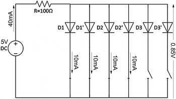
On the feed network, capacitors (C), inductors (L), and resistor (R2) are also in place. They function to DC-bias the PIN-diodes and isolate RF and DC. Also shown in Fig. 3 are PIN-diodes DC biasing pads labeled P1, GP1, GP1′, GP2, GP2′, GP3, and GP3′. Since all the three paths of the feed network are connected, input DC voltage through a wire will be applied at P1. At GP1, GP1′, GP2, GP2′, GP3, and GP3′, the DC ground wires will be soldered. The PIN-diodes which need to be forward biased for the RF signal to follow a particular path will have DC ground wires connected to the actual ground terminal of DC battery through a closed DC switch. PIN-diodes which have to remain reverse biased will have their DC ground wires disconnected from the DC battery ground through an open DC switch. This is illustrated in Fig. 5 for the case of 120° and 300° steering.
Feed side PIN-diodes circuital representation for the case of 120° and 300° steering.

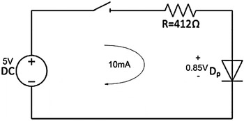
For PIN-diodes on the radiating side of the antenna, the ones which have to be forward biased are given the DC voltage through a closed DC switch and remaining are reverse biased by disconnecting DC source from them by opening the DC switch, illustrated in Fig. 6. DP represents parasitic patch's PIN-diode.
Radiating side PIN-diode circuital representation.

IV. SIMULATION AND MEASUREMENT RESULTS
Since the structure is an aperture-coupled antenna, it has two substrates. The top substrate is Rogers RT/Duroid 5880 with ε r = 2.2, tan δ = 0.0009, height of 1.575 mm, and copper cladding of 35 µm. The lower substrate over which the feed network is designed is Taconic TLC-32 with ε r = 3.2, tan δ = 0.003, height of 0.79 mm, and copper cladding of 35 µm. Resistors R1 and R2 are 412 and 100 Ω, respectively. All capacitors are C = 1 nF. The inductor used is Panasonic ELJQE56NGFA having L = 56 nH at test frequency of 100 MHz with minimum SRF of 2.5 GHz. The pin diodes used as RF switches are Skyworks SMP1320-079LF.
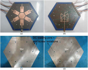
Analytical solution of mutual coupling among the array elements is a difficult task, hence a finite-element method-based numerical modeling was implemented by high-frequency structure simulator v.13. All the elements of the antenna were designed for the resonant frequency of 2.45 GHz. Width of parasitic patch was reduced so as to easily fit into the configuration as shown in Fig. 1. Separation between the hexagonal patch and parasitic patches, d, was set to 4 mm keeping under consideration the mutual coupling level, antenna gain and far-field radiation patterns. Besides, parametric analysis was performed over the stub lengths of the feed network to optimize the return loss in various steering directions. The difference in the stub lengths can be attributed to the behavior of PIN-diodes since they do not offer perfect conduction and isolation when forward and reverse biased, respectively. Path2 and Path3 are identical, whereas Path1 is not identical to Path2 and Path3. For a specific surface current orientation to be excited on the active element, the feed network paths have to be directed this way, due to which an inherent (design dictated) asymmetry as arisen between Path2, Path3 and Path1. To be more elaborate, RF signal on Path1 at junction J has symmetric paths toward D2 and D3. However, RF signal on Path2 (Path3) doesn't have such symmetry toward D1 and D3 (D1 and D2). Un-identical paths along with imperfect conduction and isolation of PIN-diodes require different stub lengths for desired resonance in various steering directions. Henceforth, stub lengths S T2 and S T3 are of equal length whereas S T1 is different from S T2, S T3. In simulator, PIN-diode in the forward biased state was modeled as inductance in series with a resistance. In the reverse biased state, it was modeled as a series combination of inductance with a parallel combination of resistance and capacitance. All these RLC values were taken from datasheet of the device. Top, middle, and bottom layers of the fabricated antenna are illustrated in Fig. 7. Figure 7(a) displays top side of the antenna with radiating elements. Besides feed structure, in Fig. 7(b), there are copper pads. These are there so that DC biasing pins and wires can be soldered. In Figs 7(c) and 7(d), apart from slot, there are copper isolations so that screws and DC biasing pins do not make any contact with the ground layers.
Fabricated antenna. (a) Rogers radiating side. (b) Taconic feed structure with PIN-diodes biasing wires. (c) Rogers ground layer with slot and copper isolations. (d) Taconic ground layer with slot and copper isolations.

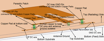
Important to note here is that the DC biasing pins are through hole pins and they are inserted in thin drilled holes where these holes extend across, from the top (radiating) side of antenna to the bottom (feed) side. This has been done so that all DC biasing wires are soldered only on one side of the antenna, i.e. the bottom side. On top side, the DC biasing pin is attached to parasitic patch's DC bias I/P point as illustrated in Fig. 8. At the bottom side, this pin is attached to a copper pad over which I/P DC wire is soldered. Similarly, another DC bias pin connects the same parasitic patch's DC GND point to another copper pad at the bottom side, to which the DC ground wire is soldered. This way, the biasing of PIN-diodes for all parasitic patches is controlled through the use of separate I/P and ground DC biasing pins. DC biasing of feed structure is simple and has been explained in the previous section. Feed structure's DC bias wires can be viewed from Fig. 7(b).
Illustration of DC bias mechanism of parasitic patch.

The extending DC wires of Figs 7(a) or 7(b) were connected to a separate PCB. This PCB consisted of open/closed DC switches for controlling the forward/reversed bias state of radiating side and feed side PIN-diodes. As a prototype design, manually controlled push buttons were utilized as DC switches. However, a microcontroller based on/off switching of DC bias through a computer program can be easily implemented.
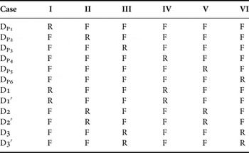
The antenna is capable of steering the main lobe in six directions. Steering is controlled as already explained in the operation mechanism; however to elaborate status (R: reverse biased, F: forward biased) of PIN-diodes for a certain steering direction, Table 1 is given. CaseI to CaseVI correspond to azimuth steering of the main lobe to 0°, 60°, 120°, 180°, 240°, and 300°, respectively. DP1 to DP6 correspond to the PIN-diodes of parasitic patches 1–6, respectively.
Status of pin diodes of radiating side and feed network to achieve desired steering.

F, forward biased; R, reverse biased.
Simulated axial ratios in directions 0° to 300° are 67.79, 37.11, 51.96, 57.1, 43.13, and 37.61 dB, respectively, which clearly indicate that antenna is linearly polarized in all directions. Cross polarization levels are −51.28, −20.37, −23.49, −43.3 XdB, −24.19 and −20.57 dB in steering directions 0° to 300°, respectively.
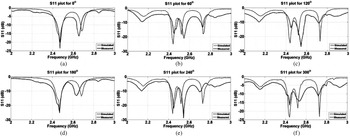
After prototype fabrication, antenna was tested with Agilent E8362B VNA. Simulated versus measured S 11 parameters for all steering directions are illustrated in Fig. 9. As shown, simulated and measured responses are in a considerable match with S 11 better than −11.5 dB for all azimuth directions The deviation between simulation and measurement results can be attributed to difference between the actual PIN-diode device and its simulated model, to the complexity of design as it incorporates a number of PIN-diodes and surface mount lumped components, and to fabrication errors and tolerance.
Simulated versus measured S 11 parameters for all steering directions. (a) 0°, (b) 60°, (c)120°, (d) 180°, (e) 240°, and (f) 300°.

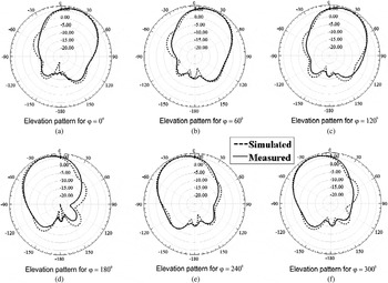
Radiation patterns of antenna were measured in anechoic chamber. Antenna was mounted on a rotating positioner as a receiving antenna. Firstly, the elevation patterns were measured for main beam azimuth angles of 0°, 60°, 120°, 180°, 240°, and 300°. The simulated versus measured elevation patterns are illustrated in Fig. 10. The results indicate that elevation patterns are almost identical in all steering angles. There is a good match between simulation and measurement results. Maximum for all elevation patterns is appearing at approximately 27° from broadside direction. The relatively lesser tilt is dominated by finiteness of antenna ground plane.
Simulated versus measured elevation plane gain patterns for all steering directions. (a) Elevation pattern for φ = 0°. (b) Elevation pattern for φ = 60°. (c) Elevation pattern for φ = 120°. (d) Elevation pattern for φ = 180°. (e) Elevation pattern for φ = 240°. (f) Elevation pattern for φ = 300°.

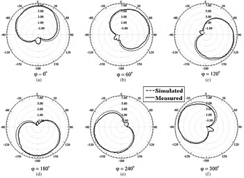
Azimuth radiation patterns were measured at elevation angle of 63° where peak gain appears and are illustrated in Fig. 11 for all steering directions. Results indicate that the main beam accurately points in desired directions. The appearance of small back lobe in all azimuth patterns can be attributed to slight positioning/alignment error of antenna during chamber measurements. Patterns are symmetric in all azimuth angles as is desired of a beam reconfigurable antenna. Simulation and measurement results have high correlation.
Simulated versus measured azimuth plane gain patterns for all steering directions. (a) φ = 0°, (b) φ = 60°, (c) φ = 120°, (d) φ = 180°, (e) φ = 240°, and (f) φ = 300°.

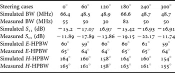
Peak gain of the proposed antenna appears at an approximate 27° tilt from broadside direction. The measured peak gain is 7.06 dB for φ = 0° case where variations in measured gain are <1 dB for the rest cases. Table 2 compares the simulated versus measured values for E/H plane half power beam width (HPBW), bandwidth (BW), and S 11 for all steering cases.
Simulated versus measured BW, S 11, and HPBW.

V. CONCLUSION
Aperture-coupled antenna with a unique feed structure for beam-switching application has been presented in this paper. Beam steering can be achieved by controlling the surface current orientation of the driven element through this feed structure. If designed with only the driven element (no parasitic patches) and feed structure, the antenna can be utilized at places dominated by high polarization mismatch losses, where such losses can be reduced by switching among various surface current orientations. Simulated versus measured results support the applicability and performance of this prototype antenna. Aperture-coupled nature gives the advantage that this structure can be integrated with other microwave circuitry due to ample space at feed side. Due to planar structure of the antenna, it has great potential to be incorporated into wireless communication terminals.
 Hassan Umair did B.E. and M.S. in Electrical (Telecommunication) Engineering from Military College of Signals (MCS), National University of Sciences and Technology (NUST), Pakistan in 2010 and 2015, respectively. Currently he is serving as visiting faculty in EE Department, MCS, NUST. His research interests include electronic beam steering, frequency selective surfaces, and RF front end design.
 Niaz Muhammad received his Bachelors degree in Computer Systems Engineering from the University of Engineering and Technology (UET), Peshawar, Pakistan in 2011. Currently he is pursuing Masters in Electrical (Telecommunication) Engineering from Military College of Signals (MCS), National University of Sciences and Technology (NUST), Pakistan. His research interests include microstrip patch antennas, frequency selective surfaces, and low noise amplifiers.
 Tayyab Hassan earned a Bachelors in Electrical (Telecommunication) Engineering from Military College of Signals (MCS), National University of Sciences and Technology (NUST), Pakistan in 2010. Afterwards he joined the Advanced Electromagnetic Systems Group at Center of Excellence in Science and Applied Technologies (CESAT), Pakistan where he is currently involved in antenna design and development. His research interests include ESPAR Antenna, conventional phased array antennas, and reconfigurable front-ends.
 Imran Rashid did his B.E. in Electrical (Telecommunication) Engineering from Military College of Signals (MCS), National University of Sciences and Technology (NUST), Pakistan, in 1999. He received his M.Sc. degree in Telecomm Engineering (Optical Communication) from D.T.U Denmark in 2004 and his Ph.D. degree in Mobile Communication from the University of Manchester, UK in 2011. Currently, he is the Head of Department at Electrical Engineering Department, MCS, NUST, Pakistan.
 Farooq A. Bhatti did Ph.D. in RF Electronics from Shanghai University of Sciences and Technology, China in 1992 and Post Doc. from UMIST, UK in 2006. Currently he is serving as an Associate Professor in EE Department, Military College of Signals (MCS), National University of Sciences and Technology (NUST), Pakistan. His research areas are antennas and microwave and millimeter wave circuit design.