I. INTRODUCTION
Frequency selective surfaces (FSSs) are very well-known devices for the spatial filtering of electromagnetic waves, which consist of two- or three-dimensional periodic array of resonant metallic elements or apertures in metallic screens printed on the dielectric substrate and used in various applications, such as radomes, sub-reflectors of antennas, telecommunications, and wireless security [Reference Vardaxoglou1]. For secondary or higher ordered grating lobe suppression, according to the diffraction theory, the size and periodicity of the resonant elements should be smaller than the wavelength of the incident radiation, otherwise the resonant optical properties of the FSS structure may be related to the coupling between adjacent elements, thus depending on the angle-of-incidence (AOI) of the incoming waves. However, for wireless security purposes, FSSs have been incorporated into the walls of buildings, which block the wireless local area network (WLAN) signals while passing the cellular phone signals [Reference Ghaffer, Kenneth, Karu, Andrew and Panagamuwa2]. Several resonant classical shapes for FSS design, for example, a circular loop [Reference Taylor, Bathelor and Parker3], square loop [Reference Li4, Reference Jha, Singh and Jyoti5], hexagonal [Reference Zheng, Yin and Ren6], and fractal geometries [Reference Xue, Gong, Zhang, Wang and Zhang7, Reference Zhang, Yin and Ma8] have been discussed based on the applications. Recently, the primary issue is to design a FSS, which is miniaturized and must be stable over the large AOI. To deal with these issues, the circular ring element topology, among the various classical shapes, is the most appropriate choice because it offers better performance in terms of the angular stability, cross-polarization, reflection/transmission bandwidth, and band separation [Reference Parker and Hamdy9–Reference Huang, Wu and Lee11]. Owing to its symmetrical nature, the resonance occurs in either of the two orthogonal coordinates and it supports a pair of degenerate modes that can have same resonant frequencies with the orthogonal field distributions [Reference Taylor, Parker and Batchelor12].
To enhance the performance of FSS's to ensure the aforementioned issues, several researchers have investigated loaded FSSs [Reference Taylor, Bathelor and Parker3, Reference Xu, Zhao, Zong and Wu13–Reference Guang-Ming, Jun-Gang and Jin-Ming21], which have been classified as active loaded and passive loaded FSSs. An active loaded FSS has been designed by implementing a tuning circuit as a part of the FSS pattern to switch the frequency response (reflections and transmission) from transmission to reflection and vice versa over the chosen frequency range [Reference Ucar, Sondas and Erdemli14]. In [Reference Chang, Langley and Parker15], an active loaded FSS was designed using PIN diodes between the FSS elements with DC magnetic biasing using a ferrite substrate to ensure the loading effect, which tunes the resonant frequency over a wide range and also switches the frequency response. In [Reference Martynyuk, Lopez and Martynyuk16], the loading was achieved through varactor diodes, which act as capacitive loading in the ring and makes the FSS structure tunable. In [Reference Mias17], Mias achieved loading through the surface mounted reactive lumped element, which shifts the bandstop frequency from a higher to a lower value and vice versa. However, these types of structures are difficult to fabricate because of the complexity and cost of fabrication [Reference Munk18]. On the other hand, passive loaded FSSs are also of significant importance because the reflection and transmission bandwidth as well as the resonant frequency is less sensitive to the angle of the plane wave incidence and the fabrication is easier due to the reduced complexity and cost of fabrication as compared to that of the active-loaded FSS structure. Various researchers [Reference Munk18–Reference Guang-Ming, Jun-Gang and Jin-Ming21] have studied the passive element-loaded FSS structures. In [Reference Guo, Sun and Lu20], the passively loaded slot elements have been discussed to achieve the dual-band FSS structures, which significantly improve the bandwidth. Recently, a FSS structure having a four-legged loaded element array with a thick dielectric substrate has been discussed [Reference Guang-Ming, Jun-Gang and Jin-Ming21], which has provided better angular stability as compared to that of the unloaded FSS structure.
In this paper, we have proposed an azimuthally periodic wedge-shaped metal-vane loaded circular-ring FSS structure, which is achieved through passive (conductive) loading of the classical circular ring to modify the electrical response of the structure, such as the chosen resonance frequency and reflection/transmission parameters with a more compact element. Recently, we had reported the synthesis technique of a circular ring FSS, which is used to obtain the physical parameters of the structure for a chosen resonance frequency [Reference Garima Bharti, Jha and Jyoti22]. We have also extended the previously reported work [Reference Garima Bharti, Jha and Jyoti22] for the synthesis of the proposed structure, which maintains a high degree of the angular stability and controlled bandwidth for satellite communications and has been designed in Ku band (12–18 GHz) of the electromagnetic spectrum. This paper is organized as follows. Section II describes the theory of operation and numerical analysis. Section III discusses the numerical optimization of structural parameters to enhance the performance of the proposed structure. Section IV discusses the effect of the number of vanes on the electrical performance of the proposed FSS structure. In Section V, the bandwidth control and angular sensitivity of the proposed structure have been discussed and compared with the classical circular ring element topology. Finally, Section VI concludes the work and discusses the future directions.
II. THEORY OF OPERATION AND NUMERICAL ANALYSIS
The angular stability is the primary aspect to design a FSS structure for satellite communications and without it the design remains unaccomplished [Reference Huang, Wu and Lee11]. For this purpose, the classical circular ring element topology is the prominent choice to improve the angular stability. In this paper, we have discussed a square loop as shown in Fig. 1(a) and circular ring as shown in Fig. 1(b) using the same values of the periodicity (p), loop size (d), and width of the conducting strip (w), which is obtained through the synthesis process as discussed in [Reference Garima Bharti, Jha and Jyoti22]. To resonate the square-loop FSS element, the size of each half loop must be a multiple of the half wavelength because each half loop acts as a dipole and in other words, the size of the square loop (d) must be a multiple of one full wavelength [Reference Huang, Wu and Lee11]. However, it does not provide an accurate prediction because practically the resonant wavelength in the square-loop FSS structure varies from 3.9d to 4.5d [Reference Langley and Parker23]. In addition, to resonate the circular ring FSS element, the mean circumference of the circular ring element must be equal to the unit wavelength and for a circular ring element printed on a dielectric substrate, the electrical length of the circumference must be equal to the unit wavelength, whereas the physical circumference becomes less than unit free-space wavelength [Reference Langley and Parker23]. To avoid the higher order grating lobes, FSS structures have been designed with the element sizes and spacing smaller than the half of the free-space wavelength at the frequency of operation. Therefore, in practice, the ratio of the perimeter of square loop (P SL) to the circumference of circular ring (C ring) is approximately equal to the ratio of the resonant frequency of the circular ring to that of the square loop and is given as follows:
 $$\displaystyle{{{P_{SL}}} \over {{C_{ring}}}} \;\cong\; \displaystyle{{{f_{{r_2}}}} \over {{f_{{r_1}}}}}\comma \;$$
where, f r 1 and f r 2 are the resonant frequencies of the square loop and circular ring FSS element, respectively. In the present analysis, the ratio of perimeter of the square loop (P SL) to the circumference of circular ring (C ring) is equal to the 1.12 times the ratio of the resonant frequency of the circular ring to that of the square loop, which is given by:
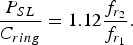 $$\displaystyle{{{P_{SL}}} \over {{C_{ring}}}} = 1.12\displaystyle{{{f_{{r_2}}}} \over {{f_{{r_1}}}}}.$$
The geometrical structure of the FSS (a) square loop, (b) circular ring, and (c) azimuthally periodic wedge-shaped metal vane loaded circular ring.

From equation (1), we have computed the resonant frequency of the circular ring (f r 2) and achieved that the circular ring FSS structure always resonates at a higher frequency than that of the square-loop FSS structure because in the array of FSS structure, for the same value of the loop size (d), the gap capacitance is less in case of the array of the circular ring as compared to that of square loop. Furthermore, comparison of the resonant frequency of the square loop and circular ring FSS structure through CST Microwave Studio and Ansoft high frequency structural simulators (HFSS) have been demonstrated in Fig. 2 and in Table 1, which reveal that the circular ring FSS structure resonates at a frequency of approximately 2 GHz higher than that of the square-loop FSS; and the ratio of perimeter of the square loop and the circumference of circular ring is equal to 1.27. In addition, there is remarkable relative error between the resonant frequencies obtained through CST Microwave Studio and Ansoft HFSS, as demonstrated in Figs. 2(a) and 2(b), respectively, as well as in Table 1. This is because of the different computational techniques used in commercially available simulators, CST Microwave Studio and Ansoft HFSS. Moreover, decrease in the resonant frequency results in the enlargement of the size of the circular ring, which restricts the miniaturization of the structure. To overcome this constraint as well as to achieve better angular stability and bandwidth control, the classical circular ring structure as shown in Fig. 1(b) has been modified as the proposed structure shown in Fig. 1(c). In [Reference Garima Bharti, Jha and Jyoti22], we have used the range of w/λ for which the correction factor (K g) has value equal to unity (as discussed in Table A1 of Appendix-A) to compute the geometrical parameters of the proposed structure. We obtained the geometrical parameters of the proposed structure in Ku band, such as periodicity (p) = 16.39 mm, outer radius of the circular ring (r 3) = 2.6 mm, inner radius of the ring or outer radius of the wedge-shaped vane (r 2) = 2.4 mm. However, the inner radius of the wedge-shaped vane (r 1) has been chosen to be equal to the 2.0 mm. An azimuthally periodic wedge-shaped metal vane loaded circular ring made of aluminium having electrical conductivity (σ) = 3.5 × 10⁷ S/m and magnetic permeability (μ) = 1.2566 × 10⁻⁶ H/m is placed on a Teflon substrate with relative dielectric permittivity of 2.02 and loss tangent (δ) of 0.002 is shown in Fig. 1(c). The thickness of dielectric substrate and wedge-shaped metallic ring for the Ku band has been computed as 1.00 and 0.00235 mm, respectively. In [Reference Munk24], it is demonstrated that with the variations in the geometrical structure of the FSS structure, the resonance frequency also changes significantly.
Comparison of the resonant frequency of the square loop and circular ring FSS structure through (a) CST Microwave Studio and (b) Ansoft HFSS.
Comparison of the resonance frequency of circular and square loop FSS structure.
For the structure shown in Fig. 1(c), the inductance has been achieved by the algebraic sum of the inductance of the circular section and the inductance due to the four wedge-shaped metal vanes. The value of inductance of a circular ring can be computed by [Reference Bahl25]:
 $${L_1}\left({{\rm nH}} \right)=1.257 \times {10^{ - 6}}.a\left[{\ln \left({\displaystyle{a \over {w+t}}} \right)+0.078} \right].{K_g}\comma \;$$
where, a is the mean radius of the circular ring and is given by: a = r 3 + r 2/2, w is the width of the conducting strip, t is the thickness of the conductor and K g is the correction factor, which indicates the height of the substrate from the ground plane and is set equal to unity. In the present analysis, all the dimensions are in millimeters. Also, if the periodic elements within the FSS structure exhibit resonance characteristics, the inductive portion of the structure exhibits total transmission at frequency near the resonance frequency, whereas the capacitive portion of the structure exhibits total reflection [Reference Reed26, Reference Fernandez27]. The capacitance of the circular ring FSS structure is given as:
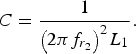 $$C=\displaystyle{1 \over {{{\left({2\pi {f_{{r_2}}}} \right)}^2}{L_1}}}.$$
For a circular ring, the value of C has been computed by substituting the value of L 1 from equation (2) and the value of f r 2 from equation (1) into equation (3). However, the value of periodicity (p), width of the conducting strip (w), and the size of the circular ring (d) are same as shown in Figs. 1(b) and 1(c), which indicates that the inter-element capacitance is same in both structures and the value of C obtained by equation (3) is used to calculate the inter element capacitance of the wedge-shaped metal vane loaded ring FSS structure. Once C is known, the change in the resonance frequency of the structure shown in Fig. 1(c) is controlled by the four wedge-shaped metal vanes and its associated inductance L 2. The inductance due to four metallic vanes is given by the modified formula, which is obtained by multiplying a constant n and a factor sinθ. The modified expression is given as:
 $$\eqalign{L_2\lpar {\rm nH}\rpar &= 2n \times 10^{ - 4} r_o \cr & \quad\left[\ln \left(\displaystyle{r_o \over {w + t}}\right)+ 1.193 + 0.333 \left(\displaystyle{{w + t} \over {r_o}}\right)\right]\sin \theta\comma} \;$$
where, n is the number of vanes. In the present analysis, the value of n is 4 and w is the width of the conducting strip. In equation (4), r o is the length of the arc of the metal vanes as shown in Fig. 1(c), and t is the thickness of the conductor. However, the value of r o for different cases approaches unity; hence to simplify the analysis, we have assumed that the value of r o is equal to unity. The total inductance (L) is the sum of L 1 and L 2. The value of L 1 is due to the diameter of the circular ring and it is obtained by using equation (2). In addition to this, there are four wedge-shaped metallic vanes, which have been used to control the value of L 2. However, the overall inductance of the azimuthally periodic wedge-shaped vane loaded structure has been given by:
 $$L = {L_1} + {L_2}.$$
The resonant frequency (f r) of azimuthally periodic wedge-shaped metallic vane FSS structure is given as:  $f_r={1 / {2\pi \sqrt {LC} }}$. For any value except the inner radius of the wedge-shaped vane (r 1) is equal to zero, L > L 1, otherwise L = L 1.
III. NUMERICAL OPTIMIZATION OF THE STRUCTURAL PARAMETERS
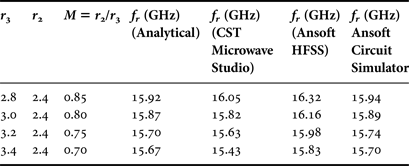
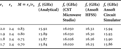
To improve the performance of the proposed FSS structure, we have performed the radial optimization of the structure for several values of M, where M is the ratio of the inner radius (r 2) to the outer radius (r 3) of the proposed structure as shown in Fig. 1(c). Considering the minimum deviation in the resonance frequency, which is computed numerically using CST Microwave Studio, Ansoft HFSS, and Ansoft Circuit Simulator, for different values of M is shown in Tables 2 and 3.
Radial optimization keeping the width (w 2) of the wedge-shaped conducting strip is fixed and radially increasing the width (w 1) of the circular conducting strip.
Radial optimization keeping width (w 1) of the circular conducting strip fixed and radially increasing the width (w 2) of the wedge-shaped conducting strip.
Radial optimization has been achieved in two different cases: (1) the width (w 2) of the wedge-shaped conducting strip, which results from (r 2 − r 1) is fixed and radially increases the width (w 1) of the circular conducting strip, which results from (r 3 − r 2) and (2) the width (w 1) of the circular conducting strip is fixed and radially increases the width (w 2). In both aforementioned cases, the value of the periodicity (p = 16.39 mm) remains same. According to the first case, to achieve the radial optimization for different values of M by keeping the width (w 2) fixed and radially increasing the width (w 1), we computed the values of inductance and capacitance numerically and validated the results through the CST Microwave Studio, Ansoft HFSS, and Ansoft Circuit Simulator, as shown in Figs. 3(a)–3(c), respectively, and Table 2. As the width (w 1) of the conducting strip is changed as 0.4, 0.6, 0.8, and 1.0 mm, the value of L 1 also varies, which is calculated as 4.50, 4.67, 5.35 and 6.35 nH, respectively, using equation (2), and provides significant change in the overall values of the inductance. On the other hand, when the width (w 2) of the wedge-shaped conducting strip is fixed, the value of L 2 is fixed, which is calculated using equation (4).
The radial optimization of proposed structure through simulation, keeping the width (w 2) is fixed and radially increasing the width (w 1), in Ku band using (a) CST Microwave Studio, (b) Ansoft HFSS, and (c) Ansoft Circuit Simulator.
The overall values of inductance are 4.503, 4.743, 5.423 and 6.423 nH for 0.85, 0.80, 0.75, and 0.70 values of M, respectively. In this case, we have considered the change in the value of the capacitance, which is 0.0156, 0.0186, 0.0216, and 0.0230 pF, respectively, for each value of M. Figures 3(a)–3(c) and Table 2, demonstrate that with the decrease in the value of M, the resonant frequency downshifts and approaches the intended frequency, which is 15 GHz and results in the optimization of the structure.
In the second case, the radial optimization was achieved by keeping the width (w 1) fixed and radially increasing the width (w 2). Owing to the fixed value of the width (w 1), the value of L 1 (nH) remains fixed and has been calculated using equation (2), which is 6.35 nH. Moreover, with the change in the width (w 2), the value of L 2 (nH) changes, which results in the change in the overall inductance of the proposed structure. We have computed the value of the overall inductance from equation (5) which is 6.42, 6.44, 6.46, and 6.48 nH for 0.83, 0.80, 0.75, and 0.70 values of M, respectively. To simplify the analysis, we have assumed that the value of capacitance remains same, which is 0.0156 pF because during the analysis negligible change has been achieved in the value of capacitance. To validate the numerical analysis, we have simulated the proposed structure using CST Microwave Studio, Ansoft HFSS as well as Ansoft Circuit Simulator and a close agreement has been achieved between the analytical and simulation results. The Ansoft Circuit Simulator is employed throughout the paper for accounting the metallic losses in the FSS structure and the analytical technique used by Ansoft Circuit Simulator is based on the mixed potential integral equation (MPIE), which is solved by using the method-of-moment (MOM). Moreover, the MPIE expresses the electric and magnetic field as a combination of a vector and a scalar potential as discussed in [28]. The comparison of results obtained analytically, through CST Microwave Studio, Ansoft HFSS, and Ansoft Circuit Simulator has been shown in Table 3. Furthermore, Figs 4(a)–4(c) obtained through CST Microwave Studio, Ansoft HFSS, and Ansoft Circuit Simulator, respectively, have demonstrated that with the decrease in the value of M, the resonant frequency for transmission as well as for reflection parameters shifts downward, which is due to increase in the inductive effect and approaches the intended frequency of the structure. The results obtained through CST Microwave Studio, Ansoft HFSS, and Ansoft Circuit Simulator have achieved the percentage deviation of 0.8, 2.4, and 0.12%, respectively, with respect to the numerical results. The deviation in results of CST Microwave Studio, Ansoft HFSS, and numerical approach is due to the different simulation approaches.
The radial optimization of the proposed structure through the simulation, keeping width (w 1) fixed and increasing the width (w 2) by using (a) CST Microwave Studio, (b) Ansoft HFSS, and (c) Ansoft Circuit Simulator in Ku band.
IV. EFFECT OF VANES ON THE PROPOSED STRUCTURE
In Section III, we have achieved the radial optimization of the proposed structure to ensure the improved performance in terms of the reflection and transmission characteristics. In the present section, we have discussed the angular sensitivity on the proposed optimized structure through increase in the number of vanes in the proposed structure, which is shown in Fig. 1(c). However, by changing the number of vanes, the periodicity of the FSS unit-cell has been influenced and due to the periodic arrangement of vanes, the field at filter plane is described in terms of the space-harmonics, which are called as Floquet harmonics. Therefore, the total field of FSS has been expanded as the superposition of a finite number of Floquet harmonics [Reference Lockyer, Vardaxoglou and Simpkin29]. However, the proposed structure has four vanes, which are present at an angular periodicity of 45°. We have increased the number of vanes by reducing the angular interval between the vanes as well as angular width of the vanes, which result the downshift in resonant frequency and decreases the 3 dB reflection and transmission bandwidth as shown in Table 4 and Fig. 5. This variation is due to the space harmonic expansion of the field occurring because of the increase in the number of vanes in the unit-cell. Figures 5(a) and 5(b) have demonstrated that with the increase in number of vanes in the proposed structure from 4 to 6, the resonant frequency downshifts with a percentage shift of 0.375 and 0.123% through CST Microwave Studio and Ansoft HFSS, respectively. With further increase the number of vanes in the proposed structure from 6 to 8, the resonant frequency up-shifts with the percentage of 0.339 and 0.245% through CST Microwave Studio and Ansoft HFSS, respectively. In addition to this, with the increase in the number of vanes in the proposed structure from 4 to 8, the 3 dB reflection and transmission bandwidth decreases with a percentage shift of 9.92 and 9.24% through CST Microwave Studio as well as 8.63 and 7.46% through Ansoft HFSS. To validate the simulation results obtained from CST Microwave Studio and Ansoft HFSS, we have performed the analysis by replacing the value of n as 4, 6, and 8 in equation (4), which results in the overall value of the inductance as 6.420, 6.50, and 6.556 nH from equation (5), respectively. Furthermore, the values of inductance and capacitance achieved through the analytical process have been used to obtain the reflection and transmission coefficients through the Ansoft Circuit Simulator as shown in Fig. 5(c), which has demonstrated the maximum percentage shift of 0.162 and 2% in the resonant frequency with respect to that simulated by CST Microwave Studio and Ansoft HFSS, respectively. Moreover, the nature of shift in the resonant frequency remains same as demonstrated through CST Microwave Simulation and Ansoft HFSS.
The effect of increase in the number of vanes on resonance frequency and 3 dB reflection/transmission bandwidth through the (a) CST Microwave Studio, (b) Ansoft HFSS, and (c) Ansoft Circuit Simulator.
The effect of increase in the number of vanes on the resonance frequency and 3 dB reflection/transmission bandwidth.
V. EFFECT OF THE AOI OF ELECTRIC FIELD
In this section, we have discussed the angular insensitivity of the proposed structure at different AOI of the electric field such as at 0°, 10°, 30°, and 50°. The simulation results of the proposed optimized structure by CST Microwave Studio and Ansoft HFSS have demonstrated 0.04 and 0.4% up-shift in the resonant frequency, respectively, as compared to the 0° incidence which has been shown in Fig. 6(a) and 6(b). This deviation is very small as compared to 16.6 [Reference Sung30], 10 [Reference Sung, Sowerby and Williamson31], and 5.45% [Reference Hosseinipanah, Wu, Zhang, Minji and Yang32]. As we increase the AOI from 30° to 50°, the resonant frequency saturates and results in angular stability. With the increase in the AOI from 0° to 50°, the 3 dB reflection and transmission bandwidth reduces to 4.62 and 3.22%, as obtained through CST Microwave Studio, and 6.03 and 5.95% as obtained through Ansoft HFSS, respectively, which is significantly very small as compared to that reported in [Reference Guang-Ming, Jun-Gang and Jin-Ming21]. When we apply the electric field at oblique angles, the overall value of the inductance changes by a factor of cosθ as compared to the value of inductance obtained from the normal incidence electric field. The value of inductance has been computed as 6.42, 6.32, 5.55, and 4.12 nH at 0°, 10°, 30°, and 50°, respectively. However, we have computed the value of the capacitance from equation (3). Furthermore, through the computed values of the inductance and capacitance, we have obtained the reflection and transmission response by Ansoft Circuit Simulator, which has not demonstrated the saturation in resonant frequency, rather experiences a small shift up to 0.125 GHz as shown in Fig. 6(c). Moreover, the reflection parameters obtained through Ansoft Circuit Simulator have demonstrated 100% reflection over the 15–17 GHz as shown in Figs 3(c), 4(c), 5(c), and 6(c), which is due to the fact that reflection coefficient achieved through the MOM technique (on which Ansoft Circuit Simulator is based) is represented in terms of the induced current (symmetric and anti-symmetric current distributions) on the periodic elements of FSS structure, as discussed in [Reference Barlevy and Rahmat-Samii33].
The effect of electric field at different AOI on the resonant frequency and 3 dB reflection/transmission bandwidth of the proposed structure through (a) CST Microwave Studio, (b) Ansoft HFSS, and (c) Ansoft Circuit Simulator.
Moreover, the proposed azimuthally periodic wedge-shaped metal vane loaded circular ring FSS structure, which has been achieved through the passive loading of circular ring provides very significant results in terms of the angular stability and bandwidth control compared to that of the classical circular ring FSS structure as discussed in Tables 5 and 6. For the same value of the periodicity (p), outer radius (r 3), inner radius (r 2) of the classical circular ring, and width (w 1) of the circular conducting strip, we have discussed the angular stability as well as the bandwidth control for 0°, 10°, 30°, and 50° of AOI.
The effect of electric field at different AOI on the resonant frequency and 3 dB transmission/reflection bandwidth of the proposed structure.
The angular stability and 3 dB reflection as well as transmission bandwidth of the classical circular ring FSS structure.
The electrical performance comparison between the proposed conductive loaded circular ring and classical circular ring such as transmission/reflection frequency response and transmission/reflection bandwidth at different AOI are shown in Tables 5 and 6, respectively. As for the simulation results of Tables 5 and 6, it is illustrated that the downshift of the resonant frequency achieved in case of the classical circular ring FSS structure is 5.16 and 6.17%, which is significantly higher than 0.04 and 0.4% as obtained for the proposed FSS structure up to 50° of AOI with the CST Microwave Studio and Ansoft HFSS, respectively. Also, in the case of classical circular ring FSS structure, the percentage reduction in 3 dB reflection as well as transmission bandwidth is 26.55, 21.87% with the CST Microwave Studio and 26.64, 23.25% through the Ansoft HFSS, which is significantly higher than that of the 4.62, 3.22% as obtained using CST Microwave Studio and 6.03, 5.95% through Ansoft HFSS for the proposed FSS structure.
VI. CONCLUSION
In this paper, an azimuthally periodic wedge-shaped metal vane loaded circular ring FSS has been discussed, which is based on the concept of conductive loading and the synthesis process of a circular loop FSS structure has been extended to obtain the structural parameters of the proposed FSS structure such as periodicity, diameter, radius of curvature, and width of the conducting strip. Moreover, the numerical analysis has been validated through commercial simulators such as CST Microwave Studio, Ansoft HFSS and Ansoft Circuit Simulator, which have demonstrated the close agreement of the results in terms of radial optimization, reflection/transmission bandwidth, and angular stability. In addition to this, the high degree of the angular stability has been achieved in the proposed structure, which is useful in satellite communications. However, the performance of the proposed structure in terms of the angular insensitivity is much better than that previously reported in the literature [Reference Sung30–Reference Hosseinipanah, Wu, Zhang, Minji and Yang32] and with the increase in AOI up to 50°, only 0.04 and 0.4% shift in the resonant frequency has been achieved through CST Microwave Studio and Ansoft HFSS, respectively, in which the angular stability has been achieved for 30° and 50° of AOI. We have also demonstrated that the variation in the performance of the proposed FSS structure in response to the number of the vanes in unit-cell. However, the proposed structure is practically more feasible and is easy to fabricate compared to other loaded FSS structures. The complementary structure of the proposed FSS will be discussed in future communications where the effect of the slot/aperture will be discussed.
ACKNOWLEDGEMENTS
The authors sincerely acknowledge the Indian Space Research Organization vide Project no. ISRO/RES/4/579/10–11. The authors are also grateful to the anonymous reviewers and the Associate Editor for their critical comments and suggestions to improve the quality of the manuscript.
APPENDIX-A
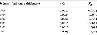
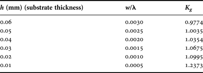
To calculate the physical parameters of the circular ring FSS structure, we have considered the importance of the correction factor (K g), which comes into picture while computing the inductance of a circular ring FSS structure. The correction term (K g) signifies the height of substrate from the ground plane. However, the substrate height from the ground plane is not considered in the FSS design. Therefore, in the presented synthesis process, the value of the correction factor is set equal to unity. The correction (K g) has been given as follows [Reference Bahl25]:
 $${K_g}=0.57 - 0.145\, \ln \left({\displaystyle{w \over h}} \right)\quad {\rm for}\, \displaystyle{w \over h}\gt 0.05\comma \;$$
where, w is the width of the conducting strip and h is the thickness of the dielectric substrate and is given as:
 $$h \sim0.05 \lambda$$
where, λ is the operating wavelength. The different values of the correction factor (K g) with the variations in the substrate thickness have been discussed in Table-A1.
We have considered the range of the w/λ in this analysis as 0.0010 ≤ w/λ ≤ 0.0025 to compute the physical parameters of the classical circular ring FSS structure. Theoretically, the ratio of the resonant frequency of the circular ring to the square loop is equal to 1.273 and through simulation, a variation was achieved. However, when we have applied the Floquet ports as excitation sources and master/slave as boundary conditions, then the ratio of resonant frequency of the circular ring to the square loop (f r 2/f r 1), for the same dimensions of the periodicity (p), loop size (d), and width of the conducting strip (w) is 1.071. On the other hand, when we applied perfect electric as well as magnetic boundary conditions and wave port as excitation sources, the ratio of resonant frequency of the circular ring to the square loop is 1.13. Therefore, the resonant frequency of a FSS structure changes with the change in the method of analysis/simulation used even when the size of the structure remain same. Furthermore, with an increase in the value of relative dielectric permittivity (εr) from 2.02 to 6.02, the ratio increases significantly.
Variation in the correction factor with the substrate thickness.
Garima Bharti completed her B. Tech. in Electronics and Communication Engineering, from the Institute of Engineering and Emerging Technologies (IEET), Baddi, Himachal Pradesh University, India and M. Tech. in Electronics and Communication Engineering from Jaypee University of Information Technology, Solan, Himachal Pradesh, India in 2010 and 2012, respectively. Currently, she is pursuing her Ph.D. from the Jaypee University of Information Technology, Solan, Himachal Pradesh, She is also working as the Project Assistant in an ISRO funded project since July 2012. Her area of interest is RF and Microwave Communication.
 Kumud Ranjan Jha completed the Under-Graduation and Post-Graduation Examinations in the Electronics and Communication Engineering branch in 1999 and 2007, respectively. Since 2007, he is an Assistant Professor in Shri Mata Vaishno Devi University, Katra, Jammu and Kashmir, India, and before joining this University, he has served in the Indian Air Force. In 2012, he was awarded with the Ph.D. degree from Jaypee University of Information Technology, Solan, Himachal Pradesh, India. Subsequently, in the same year while working on the concept of gain and directivity enhancement of the Planar Terahertz Antennas, he was awarded with the Raman Fellowship for 1 year for Post-Doctoral Study in the USA by the University Grant Commission, Government of India, New Delhi, India. He is also a visiting professor to the San Diego State University, California, USA. He has published a number of peer reviewed, research articles in international journals and conferences. His area of research is Microwave/RF passive component design and Terahertz Electronics for the future wireless communication.
Ghanshyam Singh received Ph.D. degree in Electronics Engineering from the Indian Institute of Technology, Banaras Hindu University, Varanasi, India, in 2000. He was associated with Central Electronics Engineering Research Institute, Pilani, and Institute for Plasma Research, Gandhinagar, India, respectively, where he was a Research Scientist. He had also worked as an Assistant Professor at Electronics and Communication Engineering Department, Nirma University of Science and Technology, Ahmedabad, India. He was a visiting researcher at the Seoul National University, Seoul, South Korea. At present, he is Professor at the Department of Electronics and Communication Engineering, Jaypee University of Information Technology, Wakanaghat, Solan, India. He is an author/co-author of more than 180 scientific papers of the referred journal and international conferences. His research and teaching interests include RF/Microwave Engineering, Millimeter/THz Wave Antennas and its Applications in Communication and Imaging, Next Generation Communication Systems (OFDM and Cognitive Radio), and Nanophotonics. He has more than 14 years of teaching and research experience in the area of Electromagnetic/Microwave Engineering, Wireless Communication and Nanophotonics. He has supervised various Ph.D. and M. Tech. theses. He has worked as a reviewer for several reputed journals and conferences. He is author of two books “Terahertz Planar Antennas for Next Generation Communication” and “MOSFET Technologies for Double-Pole Four-Throw Radio-Frequency Switch” published by Springer.
Rajeev Jyoti (SM'06) received the M.S. degree in Physics and the M. Tech. degree in Microwave Electronics from Delhi University, Delhi, India, in 1984 and 1986, respectively. Since 1987, he has been involved in the development of antennas for satellite communication at the Space Applications Centre (SAC), Indian Space Research Organization (ISRO), Ahmedabad, India. Presently, he is the Group Director of the Antenna Systems Group at SAC, ISRO, India. He has more than 25 years of experience in the development of space borne and ground antennas at SAC. He has contributed significantly to the design, analysis, and development of microwave antennas, especially gridded antennas, multiple beam antennas, and phased array antennas for INSAT/GSAT, RISAT, and DMSAR projects. He has published more than 55 papers in various conferences and referred journals and he holds 14 patents. He is a Fellow Member of IETE India and Chair of the Joint Chapter of IEEE AP and MTT, Ahmedabad. He was awarded the UN ESA Long Term Fellowship in Antenna and Propagation at ESTEC/ESA Noordwijk, The Netherlands.